

Philips BLF247B Datasheet

DISCRETE SEMICONDUCTORS
DATA SH EET
BLF247B
VHF push-pull power MOS
transistor
Product specification
Philips Semiconductors
August 1994

Philips Semiconductors Product specification
VHF push-pull power MOS transistor BLF247B
FEATURES
• High power gain
• Easy power control
• Good thermal stability
• Withstands full load mismatch.
APPLICATIONS
• Large signal applications in the
VHF frequency range.
DESCRIPTION
Silicon N-channel enhancement
mode vertical D-MOS push-pull
transistor encapsulated in a 4-lead,
SOT262A1 balanced flange type
package with two ceramic caps. The
mounting flange provides the
common source connection for the
transistor.
PINNING - SOT262A1
PIN CONFIGURATION
12
d
g
g
55
Top view
34
MAM098
s
d
Fig.1 Simplified outline and symbol.
CAUTION
The device is supplied in a antistatic package. The gate-source input must
be protected against static charge during transport or handling.
WARNING
PIN DESCRIPTION
1 drain 1
2 drain 2
3 gate 1
4 gate 2
5 source
Product and environmental safety - toxic materials
This product contains beryllium oxide. The product is entirely safe provided
that the BeO discs are not damaged. All persons who handle, use or dispose
of this product should be aware of its nature and of the necessary safety
precautions. After use, dispose of as chemical or special waste according to
the regulations applying at the location of the user. It must never be thrown
out with the general or domestic waste.
QUICK REFERENCE DATA
RF performance at T
MODE OF OPERATION
= 25 °C in a common source test circuit.
h
f
(MHz)
V
(V)
DS
P
(W)
L
G
(dB)
p
(%)
CW, class-B 225 28 150 ≥12 ≥55
η
D
August 1994 2
Philips Semiconductors Product specification
VHF push-pull power MOS transistor BLF247B
LIMITING VALUES
In accordance with the Absolute Maximum Rating System (IEC 134).
SYMBOL PARAMETER CONDITIONS MIN. MAX. UNIT
Per transistor section
V
DS
V
GS
I
D
P
tot
T
stg
T
j
THERMAL CHARACTERISTICS
SYMBOL PARAMETER CONDITIONS VALUE UNIT
R
th j-mb
R
th mb-h
drain-source voltage (DC) − 65 V
gate-source voltage −±20 V
drain current (DC) − 13 A
total power dissipation up to Tmb= 25 °C; total device;
− 280 W
both sections equally loaded
storage temperature −65 +150 °C
operating junction temperature − +200 °C
thermal resistance from junction to
mounting base
thermal resistance from mounting base
to heatsink
total device; both sections equally
loaded
total device; both sections equally
loaded
0.63 K/W
0.15 K/W
2
10
I
D
(A)
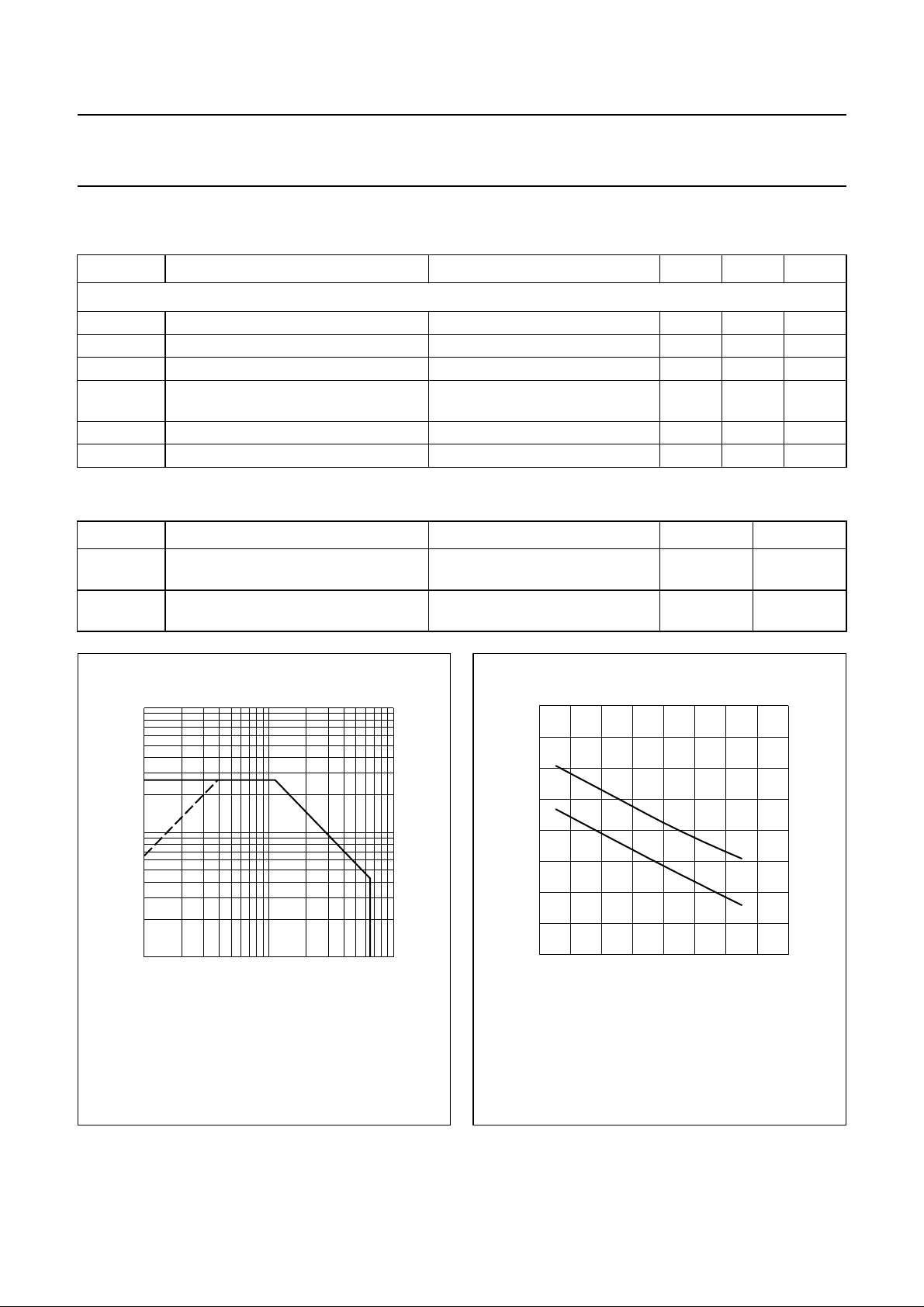
(1) (2)
10
1
Total device; both sections equally loaded.
(1) Current in this area may be limited by R
(2) Tmb=25°C.
101
Fig.2 DC SOAR.
V (V)
DS
.
DSon
MBD287
400
P
tot
(W)
300
(2)
200
(1)
100
2
10
0
040
Total device; both sections equally loaded.
(1) Continuous operation.
(2) Short-time operation during mismatch.
80 120 160
MBD288
o
T ( C)
h
Fig.3 Power derating curves.
August 1994 3
Philips Semiconductors Product specification
VHF push-pull power MOS transistor BLF247B
CHARACTERISTICS
T
=25°C unless otherwise specified.
j
SYMBOL PARAMETER CONDITIONS MIN. TYP. MAX. UNIT
Per transistor section
V
(BR)DSS
I
DSS
I
GSS
V
GSth
g
fs
R
DSon
I
DSX
C
is
C
os
C
rs
drain-source breakdown
voltage
drain-source leakage current VGS= 0; VDS=28V −−2.5 mA
gate-source leakage current VGS= ±20 V; VDS=0 −−1µA
gate-source threshold voltage ID= 50 mA; VDS=10V 2 − 4.5 V
forward transconductance ID= 5 A; VGS=10V 3 4.2 − S
drain-source on-state
resistance
drain cut-off current VGS= 10 V; VDS=10V − 22 − A
input capacitance VGS= 0; VDS=28V; f=1MHz − 225 − pF
output capacitance VGS= 0; VDS=28V; f=1MHz − 180 − pF
reverse transfer capacitance VGS= 0; VDS=28V; f=1MHz − 25 − pF
ID= 50 mA; VGS=0 65 −−V
ID= 5 A; VGS=10V − 0.2 0.3 Ω
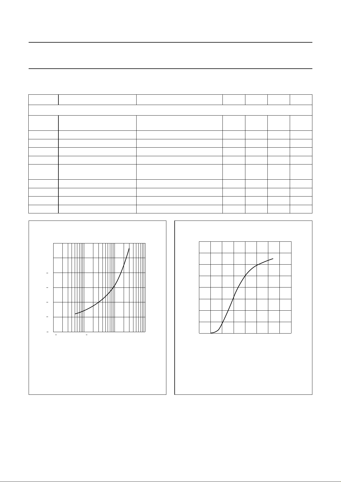
handbook, halfpage
1
TC
(mV/K)
0
1
2
3
4
5
10
VDS=10V.
2
1
10
110
Fig.4 Temperature coefficient of gate-source
voltage as a function of drain current,
typical values per section.
I (A)
D
MBD298
15
MBD299
V (V)
GS
40
I
D
(A)
30
20
10
0
0 5 10 20
VDS=10V.
Fig.5 Drain current as a function of gate-source
voltage, typical values per section.
August 1994 4
Philips Semiconductors Product specification
VHF push-pull power MOS transistor BLF247B
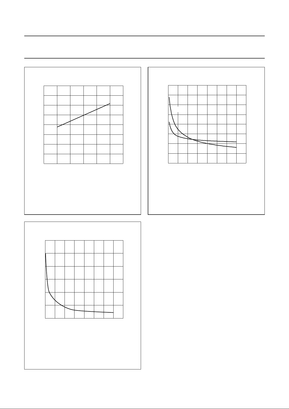
400
handbook, halfpage
R
DSon
(Ω)
300
200
100
0
050
ID= 5A; VGS=10V.
100
Fig.6 Drain-source on-state resistance as a
function of junction temperature, typical
values per section.
MBD297
o
T ( C)
j
150
C
MRA930
is
DS
(V)V
800
C
(pF)
600
C
os
400
200
0
010203040
VGS= 0; f = 1 MHz.
Fig.7 Input and output capacitance as functions
of drain-source voltage, typical values
per section.
300
C
rs
(pF)
200
100
0
0
VGS= 0; f = 1 MHz.
10 20 30 40
MBD296
V (V)
DS
Fig.8 Reverse transfer capacitance as a
function of drain-source voltage, typical
values per section.
August 1994 5
 Loading...