

Philips BLF246 Datasheet

DISCRETE SEMICONDUCTORS
DATA SH EET
BLF246
VHF power MOS transistor
Product specification
Supersedes data of September 1992
1996 Oct 21
Philips Semiconductors Product specification
VHF power MOS transistor BLF246
FEATURES
• High power gain
• Low noise figure
• Easy power control
• Good thermal stability
• Withstands full load mismatch.
APPLICATIONS
• Large signal amplifier applications in the VHF frequency
range.
DESCRIPTION
Silicon N-channel enhancement mode vertical D-MOS
transistor encapsulated in a 4-lead, SOT121 flange
package, with a ceramic cap. All leads are isolated from
the flange. A marking code, showing gate-source voltage
) information is provided for matched pair
(V
GS
applications. Refer to the General section of Data
Handbook SC19a for further information.
CAUTION
The device is supplied in an antistatic package.
The gate-source input must be protected against static
discharge during transport or handling.
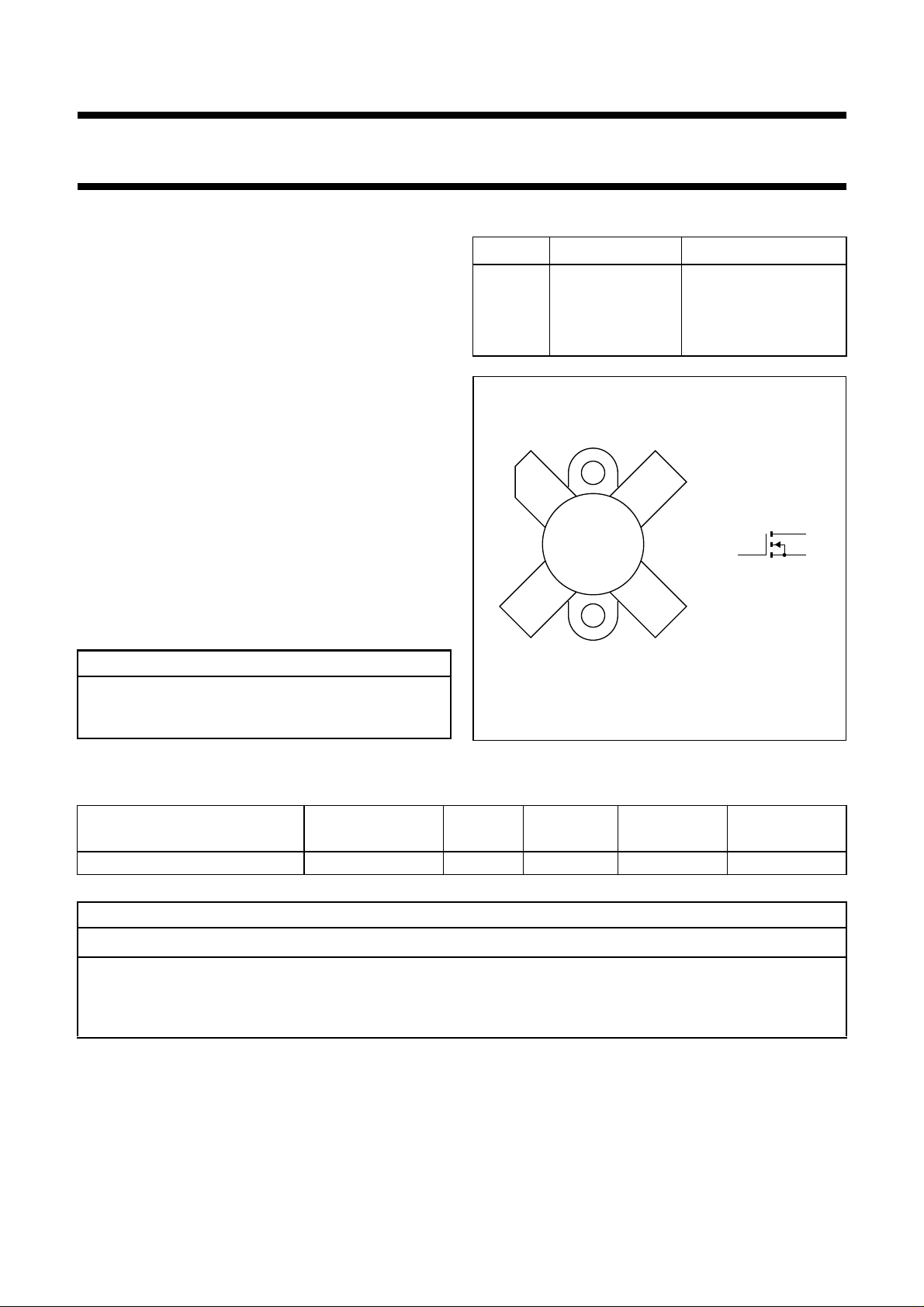
PINNING - SOT121
PIN SYMBOL DESCRIPTION
1 d drain
2 s source
3 g gate
4 s source
handbook, halfpage
14
g
32
MAM267
Fig.1 Simplified outline and symbol.
d
s
QUICK REFERENCE DATA
RF performance at T
MODE OF OPERATION
=25°C in a common source test circuit.
h
f
(MHz)
V
(V)
DS
P
(W)
L
G
p
(dB)
η
(%)
D
CW, class-B 108 28 80 ≥16 ≥55
WARNING
Product and environmental safety - toxic materials
This product contains beryllium oxide. The product is entirely safe provided that the BeO disc is not damaged.
All persons who handle, use or dispose of this product should be aware of its nature and of the necessary safety
precautions. After use, dispose of as chemical or special waste according to the regulations applying at the location of
the user. It must never be thrown out with the general or domestic waste.
1996 Oct 21 2
Philips Semiconductors Product specification
VHF power MOS transistor BLF246
LIMITING VALUES
In accordance with the Absolute Maximum System (IEC 134).
SYMBOL PARAMETER CONDITIONS MIN. MAX. UNIT
V
DS
V
GS
I
D
P
tot
T
stg
T
j
THERMAL CHARACTERISTICS
SYMBOL PARAMETER VALUE UNIT
R
th j-mb
R
th mb-h
drain-source voltage − 65 V
gate-source voltage −±20 V
DC drain current − 13 A
total power dissipation up to T
=25°C − 130 W
amb
storage temperature −65 150 °C
junction temperature − 200 °C
thermal resistance from junction to mounting base 1.35 K/W
thermal resistance from mounting base to heatsink 0.2 K/W
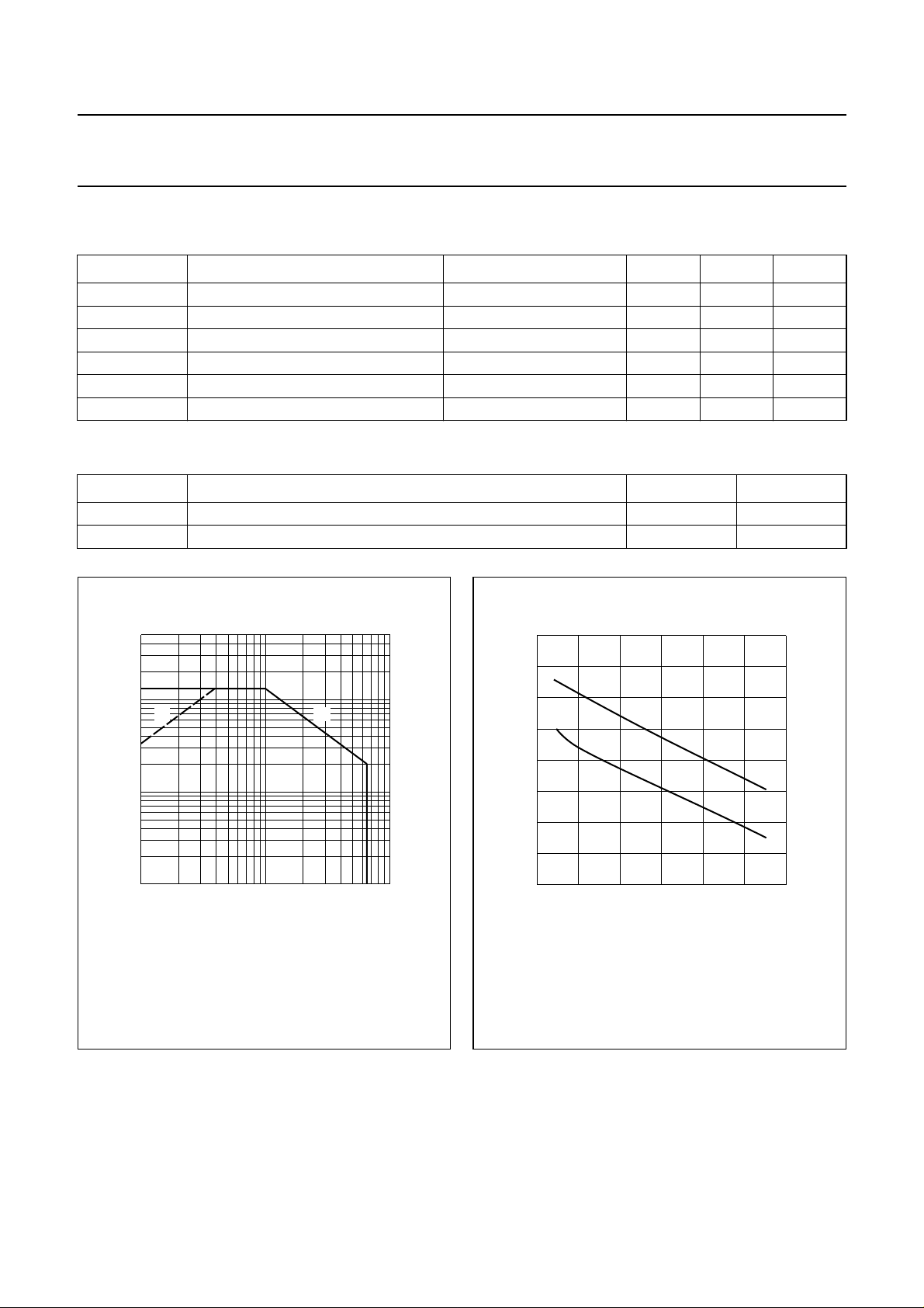
50
handbook, halfpage
I
D
(A)
10
(1)
1
−1
10
110
(1) Current is this area may be limited by R
(2) Tmb=25°C.
Fig.2 DC SOAR.
(2)
VDS (V)
DS(on)
.
MRA931
200
handbook, halfpage
P
tot
(W)
150
100
50
2
10
0
0 50 100 150
(1) Continuous operation.
(2) Short-time operation during mismatch.
(2)
(1)
MGG104
Th (°C)
Fig.3 Power derating curves.
1996 Oct 21 3
Philips Semiconductors Product specification
VHF power MOS transistor BLF246
CHARACTERISTICS
T
=25°C unless otherwise specified.
j
SYMBOL PARAMETER CONDITIONS MIN. TYP. MAX. UNIT
V
(BR)DSS
I
DSS
I
GSS
V
GSth
∆V
GS
g
fs
R
DSon
I
DSX
C
is
C
os
C
rs
drain-source breakdown voltage VGS= 0; ID=50mA 65 −−V
drain-source leakage current VGS= 0; VDS=28V −−2.5 mA
gate-source leakage current VGS= ±20 V; VDS=0 −−1µA
gate-source threshold voltage ID= 50 mA; VDS=10V 2 − 4.5 V
gate-source voltage difference of
ID= 50 mA; VDS=10V −−100 mV
matched pairs
forward transconductance ID= 2.5 A or 5 A; VDS= 10 V 3 4.2 − S
drain-source on-state resistance ID= 5 A; VGS=10V − 0.2 0.3 Ω
on-state drain current VGS= 10 V; VDS=10V − 22 − A
input capacitance VGS= 0; VDS= 28 V; f = 1 MHz − 225 − pF
output capacitance VGS= 0; VDS= 28 V; f = 1 MHz − 180 − pF
feedback capacitance VGS= 0; VDS= 28 V; f = 1 MHz − 25 − pF
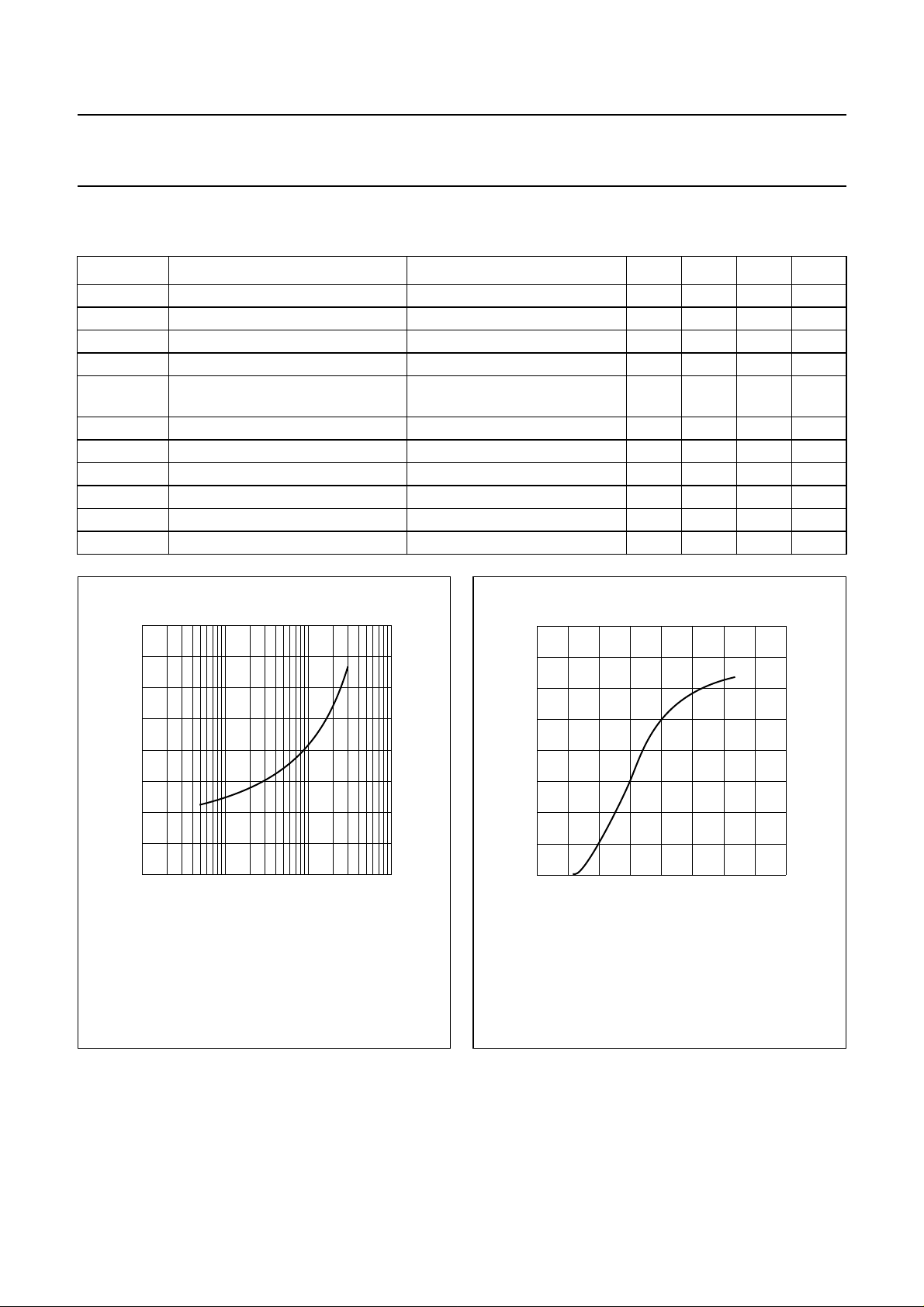
handbook, halfpage
2
T.C.
(mV/K)
0
−2
−4
−6
−2
10
VDS= 10V; valid for Th= 25 to 70 °C.
−1
10
110
ID (A)
Fig.4 Temperature coefficient of gate-source
voltage as a function of drain current, typical
values.
MGG105
40
handbook, halfpage
I
D
(A)
30
20
10
0
0 5 10 20
VDS= 10 V; Tj=25°C.
MGG106
15
VGS (V)
Fig.5 Drain current as a function of gate-source
voltage, typical values.
1996 Oct 21 4
 Loading...