

Philips BLF2047L,90 Datasheet

DATA SH EET
Product specification
Supersedes data of 2000 Feb 17
2000 Mar 06
DISCRETE SEMICONDUCTORS
BLF2047L/90
UHF power LDMOS transistor
ook, halfpage
M3D379
2000 Mar 06 2
Philips Semiconductors Product specification
UHF power LDMOS transistor BLF2047L/90
FEATURES
• High power gain
• Easy power control
• Excellent ruggedness
• Source on underside eliminates DC isolators, reducing
common mode inductance
• Designed for broadband operation (1.8 to 2.0 GHz)
• Internal input and output matching for high gain and
efficiency.
APPLICATIONS
• Common source class-AB operation for PCN and PCS
applications in the 1800 to 2000 MHz frequency range.
DESCRIPTION
Silicon N-channel enhancement mode lateral D-MOS
transistors encapsulated in a 2-lead SOT502A flange
package with a ceramic cap. The common source is
connected to the mounting flange.
PINNING
PIN DESCRIPTION
1 drain
2 gate
3 source, connected to flange
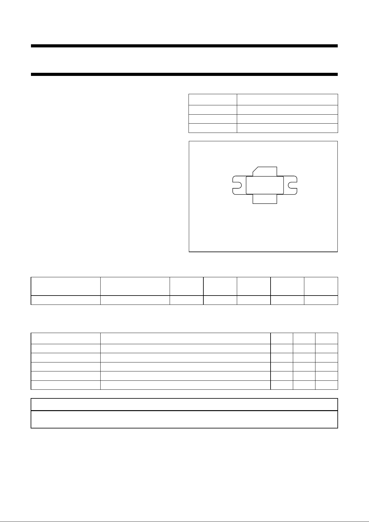
handbook, halfpage
Top view
MBK394
1
2
3
Fig.1 Simplified outline SOT502A.
QUICK REFERENCE DATA
RF performance at Th=25°C in a common source test circuit.
LIMITING VALUES
In accordance with the Absolute Maximum Rating System (IEC 60134).
MODE OF OPERATION
f
(MHz)
V
DS
(V)
P
L
(W)
G
p
(dB)
η
D
(%)
d
im
(dBc)
Two-tone, class-AB f
1
= 2000; f2= 2000.1 26 90 (PEP) >10.5 >30 ≤−25
SYMBOL PARAMETER MIN. MAX. UNIT
V
DS
drain-source voltage − 65 V
V
GS
gate-source voltage −±15 V
I
D
DC drain current − 12 A
T
stg
storage temperature −65 +150 °C
T
j
junction temperature − 200 °C
CAUTION
This product is supplied in anti-static packing to prevent damage caused by electrostatic discharge during transport
and handling. For further information, refer to Philips specs.: SNW-EQ-608, SNW-FQ-302A and SNW-FQ-302B.

2000 Mar 06 3
Philips Semiconductors Product specification
UHF power LDMOS transistor BLF2047L/90
THERMAL CHARACTERISTICS
Note
1. Determined under specified RF operating conditions, based on maximum junction temperature.
CHARACTERISTICS
T
j
=25°C unless otherwise specified.
Note
1. The value of capacitance is that of the die only.
SYMBOL PARAMETER CONDITIONS VALUE UNIT
R
th j-h
thermal resistance from junction to heatsink Th=25°C; P
tot
= 92 W; note 1 0.81 K/W
SYMBOL PARAMETER CONDITIONS MIN. TYP. MAX. UNIT
V
(BR)DSS
drain-source breakdown voltage VGS= 0; ID= 2.1 mA 65 −−V
V
GSth
gate-source threshold voltage VDS= 10 V; ID= 210 mA 1.5 − 3.5 V
I
DSS
drain-source leakage current VGS= 0; VDS=26V −−15 µA
I
DSX
on-state drain current VGS=V
GSth
+9V; VDS=10V 27 −−A
I
GSS
gate leakage current VGS= ±15 V; VDS=0 −−38 nA
g
fs
forward transconductance VDS= 10 V; ID= 7.5 A − 6.0 − S
R
DSon
drain-source on-state resistance VGS=V
GSth
+9V; ID= 7.5 A − 0.11 −Ω
C
rss
feedback capacitance VGS=0;VDS= 26 V; f = 1 MHz;
note 1
− 5.1 − pF
2000 Mar 06 4
Philips Semiconductors Product specification
UHF power LDMOS transistor BLF2047L/90
APPLICATION INFORMATION
RF performance in a common source class-AB circuit. Th=25°C; R
th j-h
= 0.81 K/W; unless otherwise specified.
Ruggedness in class-AB operation
The BLF2047L/90is capable of withstanding a load mismatch corresponding to VSWR = 10 : 1 through all phases under
the following conditions: V
DS
= 26 V; IDQ= 525 mA; PL= 90 W; f = 2000 MHz (single tone).
MODE OF OPERATION
f
(MHz)
V
DS
(V)
I
DQ
(mA)
P
L
(W)
G
p
(dB)
η
D
(%)
d
im
(dBc)
Two-tone, class-AB f
1
= 2000; f2= 2000.1 26 525 90 (PEP) >10.5 >30 ≤−25
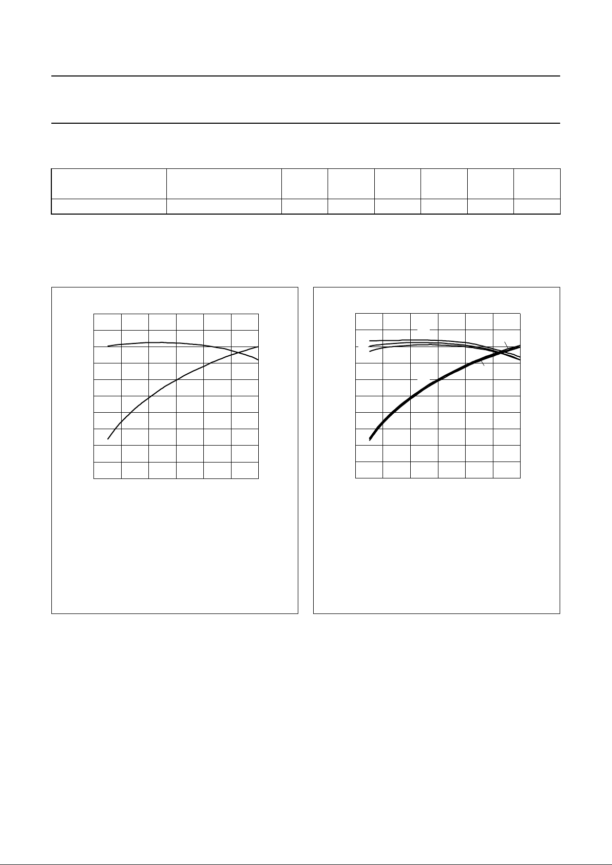
handbook, halfpage
0
PL (PEP) (W)
G
p
(dB)
G
p
40 80 120
15
5
10
η
D
(%)
η
D
50
0
10
20
30
40
MCD933
Fig.2 Powergain and drainefficiency asfunctions
of peak envelope load power; typical
values.
VDS= 26 V; IDQ= 525 mA; Th≤ 25 °C;
f
1
= 2000 MHz; f2= 2000.1 MHz.
handbook, halfpage
0
PL (PEP) (W)
G
p
(dB)
40
(1)
(1)
(3)
(3)
80 120
15
5
10
η
D
(%)
50
0
10
20
30
40
MCD928
(2)
G
p
η
D
(2)
Fig.3 Powergain and drainefficiency asfunctions
of peak envelope load power; typical
values.
VDS=26V;Th≤25 °C; f1= 2000 MHz;f2= 2000.1 MHz.
(1) IDQ= 650 mA.
(2) IDQ= 525 mA.
(3) IDQ= 400 mA.
 Loading...