

Philips BLF2047SL, BLF2047S, BLF2047 Datasheet

DATA SH EET
Product specification
Supersedes data of 1999 Jul 01
1999 Dec 02
DISCRETE SEMICONDUCTORS
BLF2047
UHF power LDMOS transistor
ook, halfpage
M3D379
1999 Dec 02 2
Philips Semiconductors Product specification
UHF power LDMOS transistor BLF2047
FEATURES
• High power gain
• Easy power control
• Excellent ruggedness
• Source on underside eliminates DC isolators, reducing
common mode inductance
• Designed for broadband operation (1.8 to 2.2 GHz).
• Internal input and output matching for high gain and
efficiency
APPLICATIONS
• Common source class-AB operation for PCN and PCS
applications in the 1800 to 2200 MHz frequency range.
DESCRIPTION
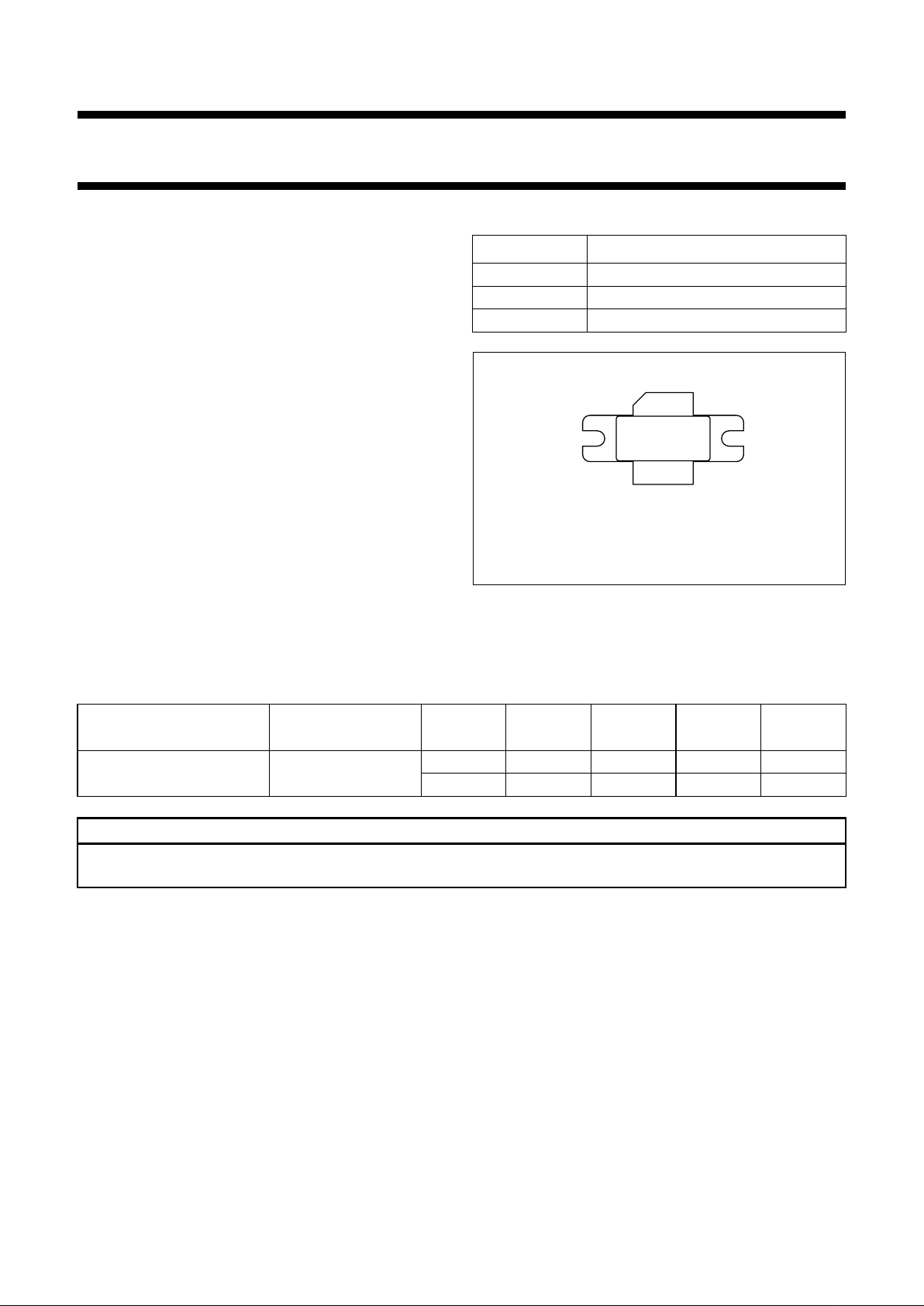
Silicon N-channel enhancement mode lateral D-MOS
transistor encapsulated in a 2-lead flange SOT502A
package with a ceramic cap. The common source is
connected to the mounting flange.
PINNING
PIN DESCRIPTION
1 drain
2 gate
3 source connected to flange
handbook, halfpage
Top view
MBK394
1
2
3
Fig.1 Simplified outline SOT502A.
QUICK REFERENCE DATA
RF performance at Th=25°C in a common source test circuit.
MODE OF OPERATION
f
(MHz)
V
DS
(V)
P
L
(W)
G
p
(dB)
η
D
(%)
d
im
(dBc)
Two-tone, class-AB f
1
= 2200; f2= 2200.1
26 65 (PEP) >10 >30 ≤−25
28 65 (PEP) typ. 12.6 typ. 31 typ. −29
CAUTION
This product is supplied in anti-static packing to prevent damage caused by electrostatic discharge during transport
and handling. For further information, refer to Philips specs.: SNW-EQ-608, SNW-FQ-302A and SNW-FQ-302B.
1999 Dec 02 3
Philips Semiconductors Product specification
UHF power LDMOS transistor BLF2047
LIMITING VALUES
In accordance with the Absolute Maximum Rating System (IEC 134).
THERMAL CHARACTERISTICS
Note
1. Determined under specified RF operating conditions, based on maximum peak junction temperature.
CHARACTERISTICS
T
j
=25°C unless otherwise specified.
SYMBOL PARAMETER MIN. MAX. UNIT
V
DS
drain-source voltage − 65 V
V
GS
gate-source voltage −±15 V
I
D
DC drain current − 9A
T
stg
storage temperature −65 +150 °C
T
j
junction temperature − 200 °C
SYMBOL PARAMETER CONDITIONS VALUE UNIT
R
th j-h
thermal resistance from junction to heatsink Th=25°C, P
tot
= 152 W, note 1 1.15 K/W
SYMBOL PARAMETER CONDITIONS MIN. TYP. MAX. UNIT
V
(BR)DSS
drain-source breakdown voltage VGS= 0; ID= 1.4 mA 65 −−V
V
GSth
gate-source threshold voltage VDS= 10 V; ID= 140 mA 1.5 − 3.5 V
I
DSS
drain-source leakage current VGS= 0; VDS=26V −−10 µA
I
DSX
on-state drain current VGS=V
GSth
+9V; VDS=10V 18 −−A
I
GSS
gate leakage current VGS= ±15 V; VDS=0 −−250 nA
g
fs
forward transconductance VDS= 10 V; ID=5A − 4 − S
R
DSon
drain-source on-state resistance VGS=V
GSth
+9V; ID=5A − 0.17 −Ω
C
rss
feedback capacitance VGS= 0; VDS= 26 V; f = 1 MHz − 3.4 − pF
1999 Dec 02 4
Philips Semiconductors Product specification
UHF power LDMOS transistor BLF2047
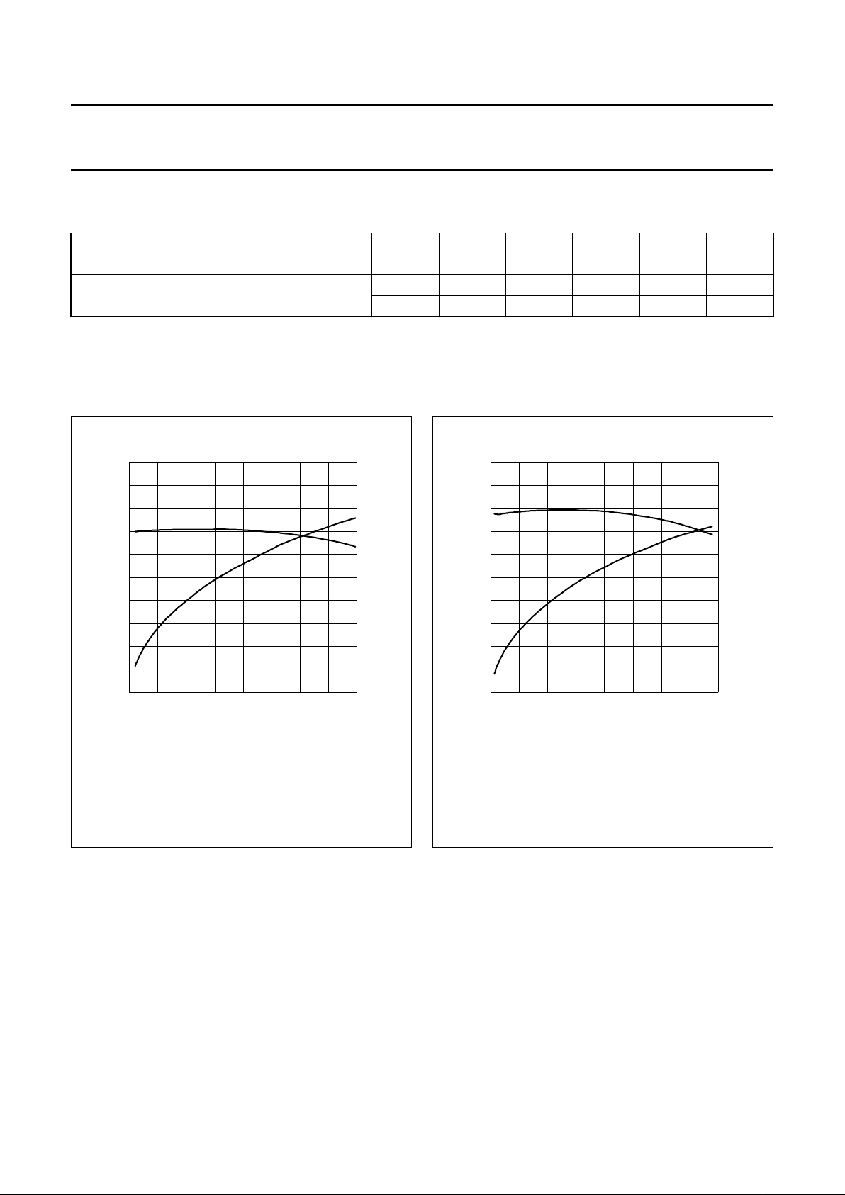
APPLICATION INFORMATION
RF performance in a common source class-AB circuit. Th=25°C; R
th j-h
= 1.15 K/W; unless otherwise specified.
Ruggedness in class-AB operation
The BLF2047is capable of withstanding a load mismatch corresponding to VSWR = 10 : 1 through all phases under the
following conditions: V
DS
= 26 V; IDQ= 400 mA; PL= 65 W (CW); f = 2200 MHz.
MODE OF OPERATION
f
(MHz)
V
DS
(V)
I
DQ
(mA)
P
L
(W)
G
p
(dB)
η
D
(%)
d
im
(dBc)
Two-tone, class-AB f
1
= 2200; f2= 2200.1
26 400 65 (PEP) >10 >30 ≤−25
28 400 65 (PEP) typ. 12.6 typ. 31 typ. −29
handbook, halfpage
02040 80
15
5
MGS914
60
10
50
0
40
30
20
10
G
p
(dB)
G
p
η
D
(%)
η
D
PL (PEP) (W)
Fig.2 Power gain and drain efficiency as functions
of peak envelope load power; typical values.
VDS= 26 V; IDQ= 400 mA; Th≤ 25 °C;
f
1
= 2000 MHz; f2= 2000.1 MHz.
handbook, halfpage
02040 80
15
5
MGS913
60
10
50
0
40
30
20
10
G
p
(dB)
G
p
η
D
(%)
η
D
PL (PEP) (W)
Fig.3 Power gain and drain efficiency as functions
of peak envelope load power; typical values.
VDS= 26 V; IDQ= 400 mA; Th≤ 25 °C;
f
1
= 2200 MHz; f2= 2200.1 MHz.
 Loading...