

Philips BLF202 Datasheet
DISCRETE SEMICONDUCTORS
DATA SH EET
M3D175
BLF202
HF/VHF power MOS transistor
Product specification 1999 Oct 20

Philips Semiconductors Product specification
HF/VHF power MOS transistor BLF202
FEATURES
• High power gain
• Easy power control
• Gold metallization
• Good thermal stability
• Withstands full load mismatch.
APPLICATIONS
• Communications transmitters inthe HF/VHF range with
a nominal supply voltage of 12.5 V.
DESCRIPTION
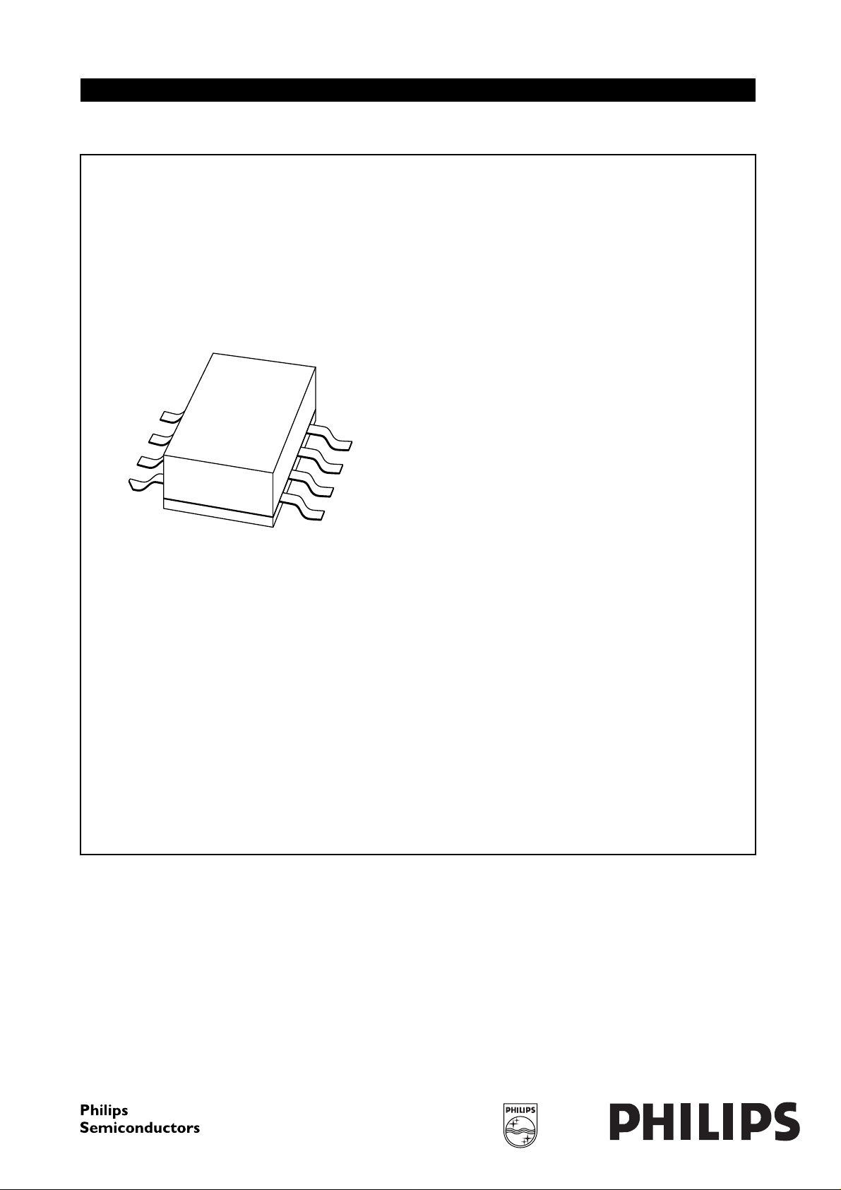
Silicon N-channel enhancement mode vertical D-MOS
transistor in an 8-lead SOT409A SMD package with a
ceramic cap.
PINNING - SOT409A
PIN DESCRIPTION
1, 8 source
2, 3 gate
4, 5 source
6, 7 drain
handbook, halfpage
Fig.1 Simplified outline.
85
14
Top view
MBK150
QUICK REFERENCE DATA
RF performance at Tmb=25°C in a common source test circuit.
MODE OF OPERATION
f
(MHz)
V
(V)
DS
P
(W)
L
G
(dB)
p
η
D
(%)
CW, class-B 175 12.5 2 >10 >50
CAUTION
This product is supplied in anti-static packing to prevent damage caused by electrostatic discharge during transport
and handling. For further information, refer to Philips specs.: SNW-EQ-608, SNW-FQ-302A, and SNW-FQ-302B.
1999 Oct 20 2
Philips Semiconductors Product specification
HF/VHF power MOS transistor BLF202
LIMITING VALUES
In accordance with the Absolute Maximum System (IEC 134).
SYMBOL PARAMETER CONDITIONS MIN. MAX. UNIT
V
DS
V
GS
I
D
P
tot
T
stg
T
j
THERMAL CHARACTERISTICS
SYMBOL PARAMETER CONDITIONS VALUE UNIT
R
th j-mb
drain-source voltage − 40 V
gate-source voltage − 20 V
DC drain current − 1A
total power dissipation Tmb≤ 85 °C − 5.7 W
storage temperature −65 150 °C
junction temperature − 200 °C
thermal resistance from junction to
Tmb≤ 85 °C, P
= 5.7 W 20.5 K/W
tot
mounting base
10
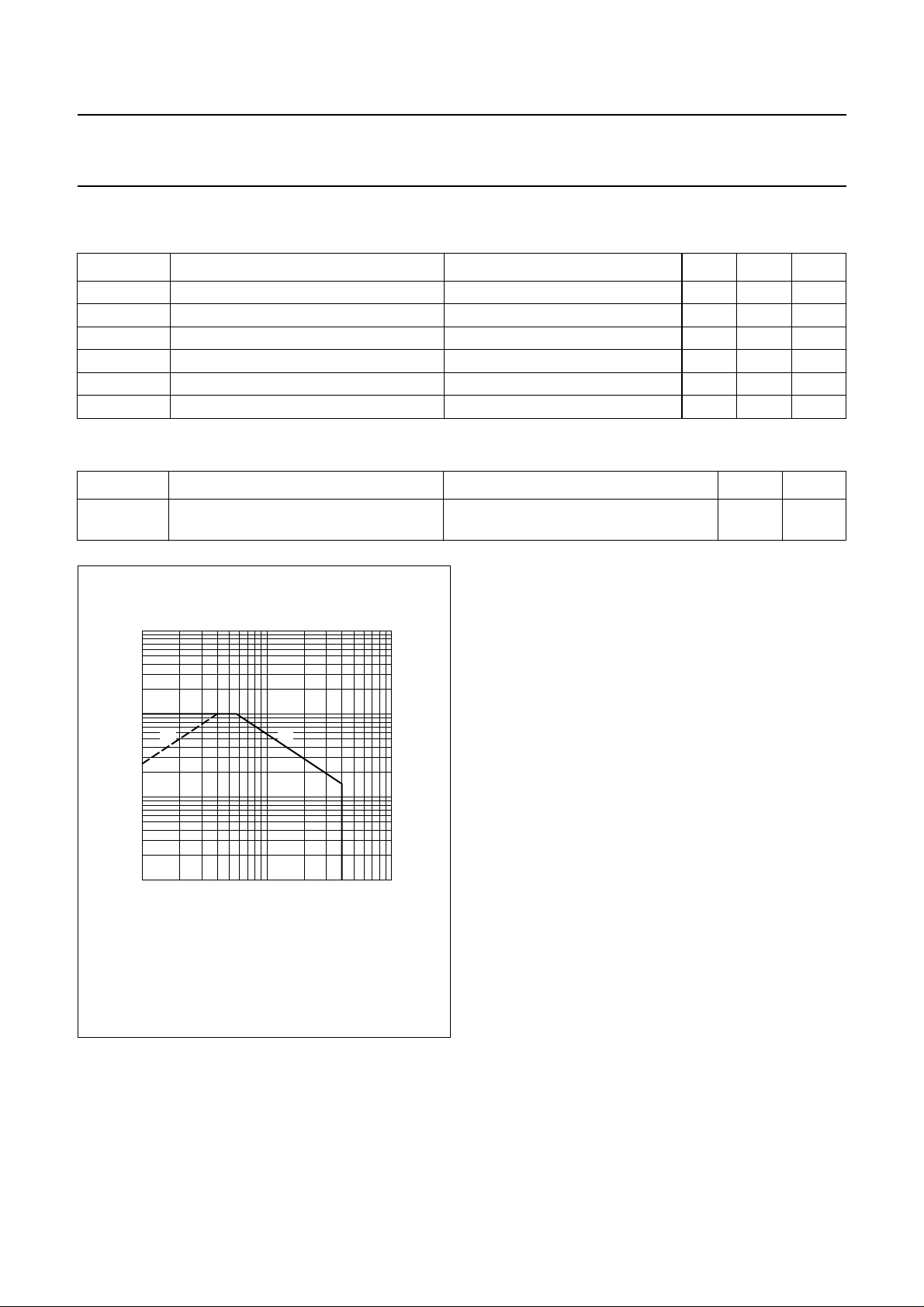
handbook, halfpage
I
D
(A)
1
(1)
−1
10
−2
10
110
(1) Current is this area may be limited by R
(2) Tmb=85°C.
Fig.2 DC SOAR.
MCD789
(2)
V
(V)
DS
.
DS(on)
2
10
1999 Oct 20 3
Philips Semiconductors Product specification
HF/VHF power MOS transistor BLF202
CHARACTERISTICS
Tj=25°C unless otherwise specified.
SYMBOL PARAMETER CONDITIONS MIN. TYP. MAX. UNIT
V
(BR)DSS
V
GS(th)
I
DSS
I
GSS
I
DSX
R
DSon
g
fs
C
is
C
os
C
rs
drain-source breakdown voltage ID= 3 mA; VGS=0 40 −− V
gate-source threshold voltage ID= 3 mA; VDS=10V 2 − 4.5 V
drain-source leakage current VGS= 0; VDS= 12.5 V −−10 µA
gate-source leakage current VGS= ±20 V; VDS=0 −−1 µA
on-state drain current VGS= 15 V; VDS=10V − 1.3 − A
drain-source on-state resistance ID= 0.3 A; VGS=15V − 3.5 4 Ω
forward transconductance ID= 0.3 A; VDS= 10 V 80 135 − mS
input capacitance VGS= 0; VDS= 12.5 V; f = 1 MHz − 5.3 − pF
output capacitance VGS= 0; VDS= 12.5 V; f = 1 MHz − 7.8 − pF
feedback capacitance VGS= 0; VDS= 12.5 V; f = 1 MHz − 1.8 − pF
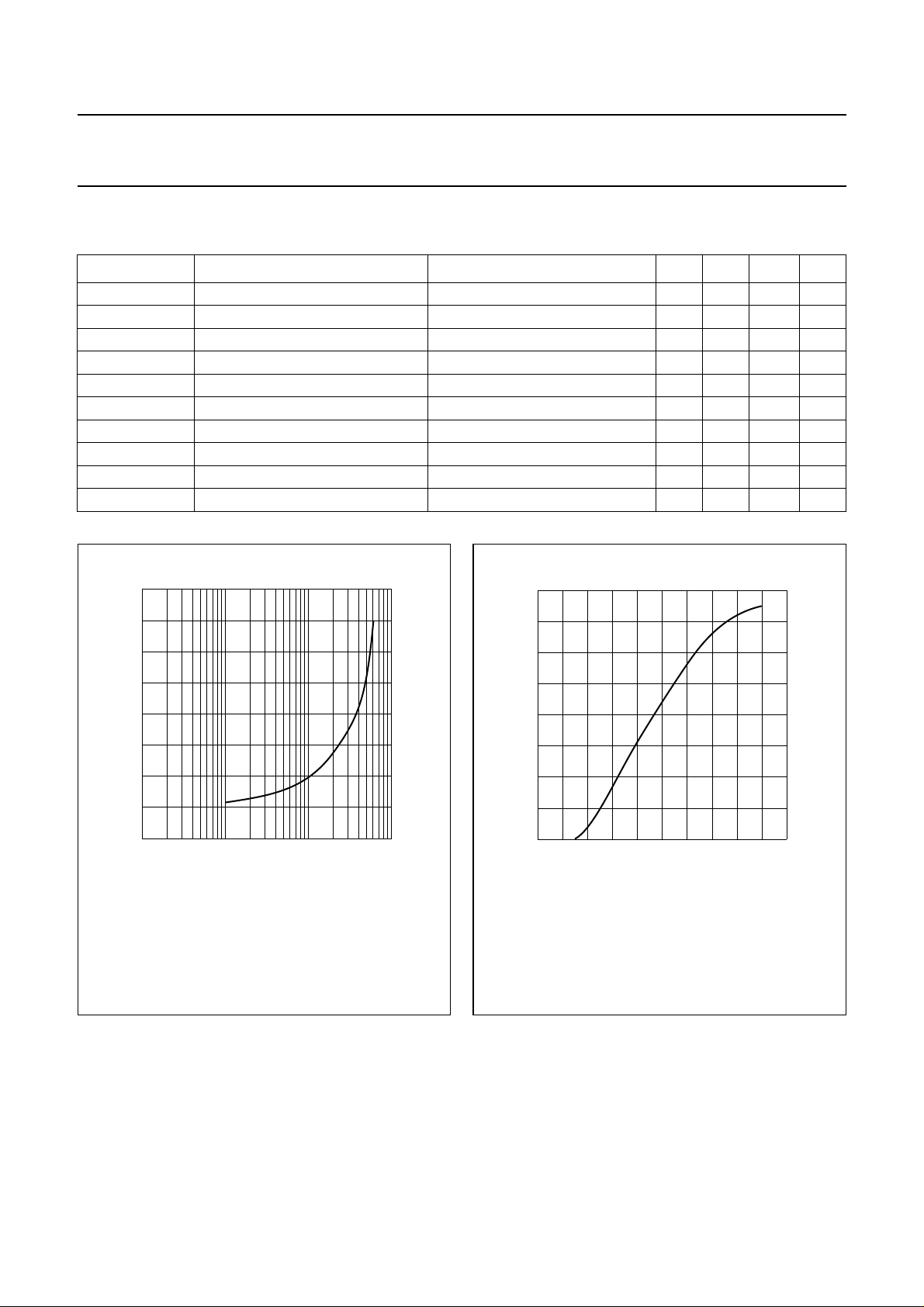
15
handbook, halfpage
T.C.
(mV/K)
10
5
0
−5
11010
VDS=10V.
2103
ID (mA)
Fig.3 Temperature coefficient of gate-source
voltageasafunctionofdrain current; typical
values.
MGP111
1600
handbook, halfpage
I
D
(mA)
1200
800
400
0
0
VDS= 10 V; Tj=25°C.
420
81216
MGP112
VGS (V)
Fig.4 Drain current as a function of gate-source
voltage; typical values.
1999 Oct 20 4
Philips Semiconductors Product specification
HF/VHF power MOS transistor BLF202
handbook, halfpage
5
R
DSon
(Ω)
4
3
2
1
0
0 40 80 160
VGS= 15 V; ID= 0.3 A.
120
Fig.5 Drain-source on-state resistance as a
function of junction temperature; typical
values.
MGP113
Tj (°C)
12
MGP114
VDS (V)
30
handbook, halfpage
C
(pF)
20
10
0
048 16
VGS= 0; f = 1 MHz.
C
os
C
is
Fig.6 Input and output capacitance as functions
of drain-source voltage; typical values.
handbook, halfpage
5
C
rs
(pF)
4
3
2
1
0
048 16
VGS= 0; f = 1 MHz.
12
VDS (V)
Fig.7 Feedback capacitance as a function of
drain-source voltage; typical values.
MGP115
1999 Oct 20 5
 Loading...