

Philips BLF1822-10 Technical data
查询BLF1822-10供应商查询BLF1822-10供应商
DISCRETE SEMICONDUCTORS
DATA SH EET
M3D381
BLF1822-10
UHF power LDMOS transistor
Product specification
Supersedes data of 2002 Mar 12
2003 Feb 10
Philips Semiconductors Product specification
UHF power LDMOS transistor BLF1822-10
FEATURES
• Typical 2-tone performance at a supply voltage of 26 V
and IDQ of 85 mA:
– Output power = 10 W (PEP)
– Gain = 18.5 dB at 900 MHz, 13.5 dB at 2200 MHz
– Efficiency = 39% at 900 MHz, 34% at 2200 MHz
– dim = −31 dBc at 900 MHz, −28 dBc at 2200 MHz
• Easy power control
• Excellent ruggedness
• High power gain
• Excellent thermal stability
• Designed for broadband operation (HF to 2200 MHz)
• No internal matching for broadband operation.
APPLICATIONS
• RF power amplifiers for GSM, EDGE, CDMA and
W-CDMA base stations and multicarrier applications in
the HF to 2200 MHz frequency range
• Broadcast drivers.
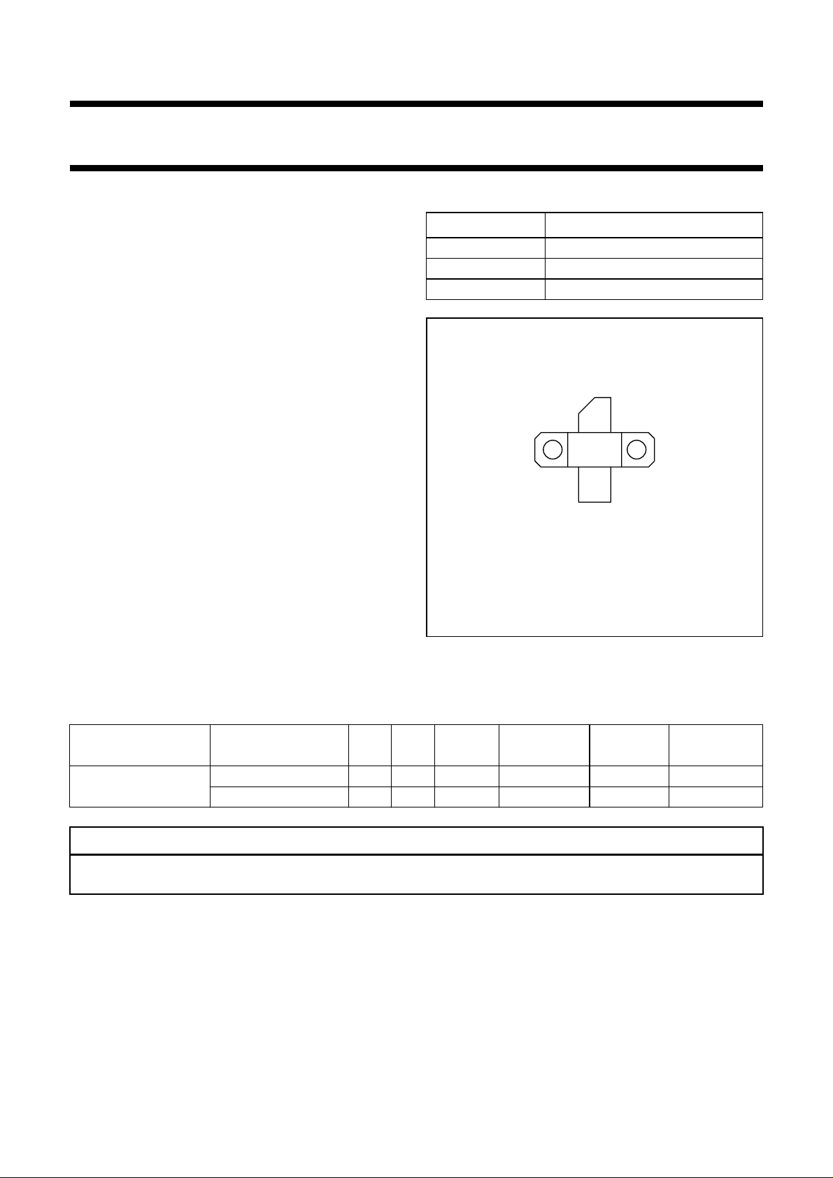
PINNING - SOT467C
PIN DESCRIPTION
1 drain
2 gate
3 source, connected to flange
Top view
1
3
2
MBK584
DESCRIPTION
Fig.1 Simplified outline.
10 W LDMOS power transistor for base station
applications at frequencies from HF to 2200 MHz.
QUICK REFERENCE DATA
RF performance at Th=25°C in a common source test circuit.
MODE OF
OPERATION
CW, class-AB (2-tone)
f
(MHz)
= 2200; f2= 2200.1 26 85 10 (PEP) >11; typ. 13.5 >30; typ. 34 ≤−26; typ. −28
f
1
f
= 960; f2= 960.1 26 85 10 (PEP) typ. 18.5 typ. 39 typ. −33
1
V
(V)
DS
I
DQ
(mA)
P
(W)
L
G
p
(dB)
η
(%)
D
d
im
(dBc)
CAUTION
This product is supplied in anti-static packing to prevent damage caused by electrostatic discharge during transport
and handling. For further information, refer to Philips specs.: SNW-EQ-608, SNW-FQ-302A and SNW-FQ-302B.
2003 Feb 10 2

Philips Semiconductors Product specification
UHF power LDMOS transistor BLF1822-10
LIMITING VALUES
In accordance with the Absolute Maximum Rating System (IEC 60134).
SYMBOL PARAMETER MIN. MAX. UNIT
V
DS
V
GS
I
D
T
stg
T
j
THERMAL CHARACTERISTICS
SYMBOL PARAMETER CONDITIONS VALUE UNIT
R
th j-mb
R
th mb-h
Note
1. Thermal resistance is determined under RF operating conditions.
drain-source voltage − 65 V
gate-source voltage −±15 V
drain current (DC) − 2.2 A
storage temperature −65 +150 °C
junction temperature − 200 °C
thermal resistance from junction to mounting base Tmb=25°C; note 1 5 K/W
thermal resistance from mounting base to heatsink 0.5 K/W
CHARACTERISTICS
Tj=25°C unless otherwise specified.
SYMBOL PARAMETER CONDITIONS MIN. TYP. MAX. UNIT
V
(BR)DSS
V
GSth
I
DSS
I
DSX
I
GSS
g
fs
R
DSon
C
is
C
os
C
rs
drain-source breakdown voltage VGS= 0; ID= 0.2 mA 65 −−V
gate-source threshold voltage VDS= 10 V; ID=20mA 4 − 5V
drain-source leakage current VGS= 0; VDS=26V −−1.5 µA
on-state drain current VGS=V
+9V; VDS=10V 2.8 −−A
GSth
gate leakage current VGS= ±15 V; VDS=0 −−40 nA
forward transconductance VDS= 10 V; ID= 0.75 A − 0.5 − S
drain-source on-state resistance VGS= 10 V; ID= 0.75 A − 1.2 −Ω
input capacitance VGS= 0; VDS= 26 V; f = 1 MHz − 13 − pF
output capacitance VGS= 0; VDS= 26 V; f = 1 MHz − 11 − pF
feedback capacitance VGS= 0; VDS= 26 V; f = 1 MHz − 0.5 − pF
2003 Feb 10 3
Philips Semiconductors Product specification
UHF power LDMOS transistor BLF1822-10
APPLICATION INFORMATION 2.2 GHz
RF performance in a common source class-AB circuit. Th=25°C; R
= 0.4 K/W; unless otherwise specified.
th mb-h
MODE OF OPERATION
CW, class-AB (2-tone) f
f
(MHz)
= 2200; f2= 2200.1 26 85 10 (PEP) >11 >30 ≤−26
1
V
(V)
DS
I
DQ
(mA)
P
(W)
L
G
p
(dB)
η
(%)
D
d
im
(dBc)
Ruggedness in class-AB operation
The BLF1822-10 iscapable of withstanding a load mismatch corresponding to VSWR = 10 : 1 through all phases under
the following conditions: V
2
10
handbook, halfpage
C
(pF)
C
os
C
is
10
C
rs
1
= 26 V; f = 2200 MHz at rated load power.
DS
MGW642
handbook, halfpage
G
(dB)
MGW643
15
G
p
10
5
p
η
D
60
40
20
η
(%)
D
−1
10
0 102030
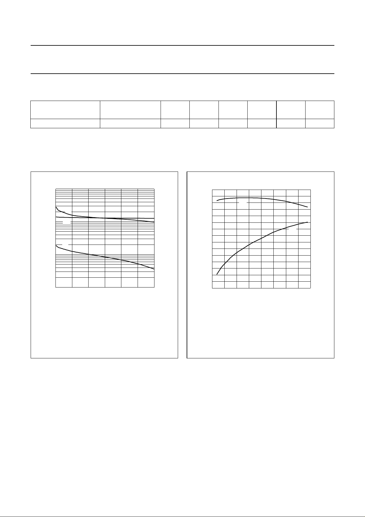
VGS= 0; f = 1 MHz.
VDS (V)
Fig.2 Input, output and feedback capacitance as
functions of drain-source voltage; typical
values.
0
0841216
VDS= 26 V; IDQ= 85 mA; Th≤ 25 °C;
= 2000 MHz; f2= 2000.1 MHz.
f
1
P
(PEP) (W)
L
0
Fig.3 Power gain and efficiency as functions of
peak envelope load power; typical values.
2003 Feb 10 4
Philips Semiconductors Product specification
UHF power LDMOS transistor BLF1822-10
handbook, halfpage
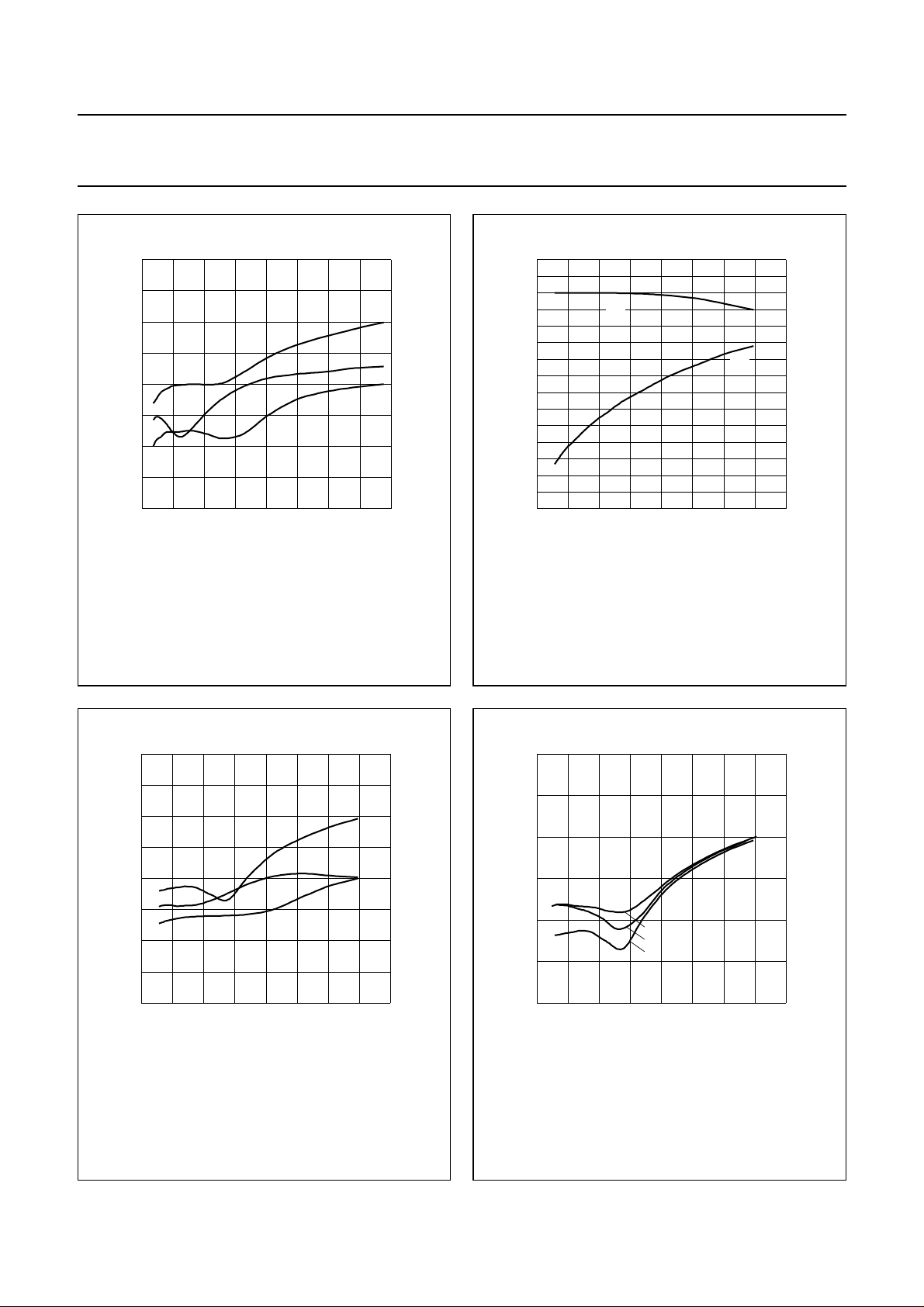
0
d
im
(dBc)
−20
−40
−60
−80
08412
VDS= 26 V; IDQ= 85 mA; Th≤ 25 °C;
= 2000 MHz; f2= 2000.1 MHz.
f
1
d
3
d
5
d
7
PL (PEP) (W)
MGW644
Fig.4 Intermodulation distortion as a function of
peak envelope load power; typical values.
MGW645
15
handbook, halfpage
G
p
(dB)
10
5
16
0
0841216
VDS= 26 V; IDQ= 85 mA;
= 2200 MHz; f2= 2200.1 MHz.
f
1
G
p
η
D
P
(PEP) (W)
L
60
40
20
0
η
(%)
D
Fig.5 Power gain and efficiency as functions of
peak envelope load power; typical values.
handbook, halfpage
0
d
im
(dBc)
−20
−40
−60
−80
08412
VDS= 26 V; IDQ= 85 mA; Th≤ 25 °C;
= 2200 MHz; f2= 2200.1 MHz.
f
1
d
3
d
5
d
7
PL (PEP) (W)
MGW646
Fig.6 Intermodulation distortion as a function of
peak envelope load power; typical values.
handbook, halfpage
16
0
d
3
(dBc)
−20
−40
−60
0841216
VDS= 26 V; Th≤ 25 °C;
= 2200 MHz; f2= 2200.1 MHz.
f
1
= 115 mA. (2) IDQ= 55 mA. (3) IDQ=85mA.
(1) I
DQ
(1)
(2)
(3)
P
L
MGW647
(PEP) (W)
Fig.7 Intermodulation distortion as a function of
peak envelope load power; typical values.
2003 Feb 10 5
 Loading...