

Philips BLF177 Datasheet

DISCRETE SEMICONDUCTORS
DATA SH EET
BLF177
HF/VHF power MOS transistor
Product specification
File under Discrete Semiconductors, SC08a
September 1992
Philips Semiconductors Product specification
HF/VHF power MOS transistor BLF177
FEATURES
• High power gain
• Low intermodulation distortion
• Easy power control
• Good thermal stability
• Withstands full load mismatch.
DESCRIPTION
Silicon N-channel enhancement
mode vertical D-MOS transistor
designed for industrial and military
applications in the HF/VHF frequency
range.
The transistor is encapsulated in a
4-lead, SOT121 flange envelope, with
a ceramic cap. All leads are isolated
from the flange.
A marking code, showing gate-source
voltage (V
) information is provided
GS
for matched pair applications. Refer
to the 'General' section for further
information.
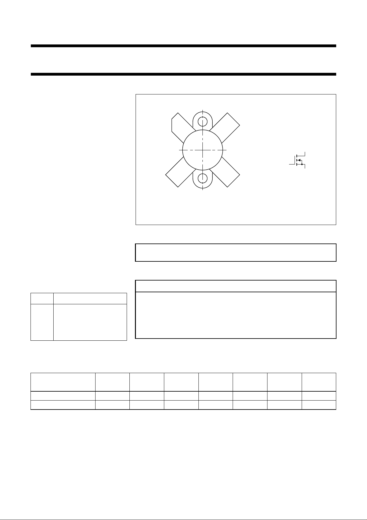
PIN CONFIGURATION
ndbook, halfpage
14
g
MBB072
32
MLA876
d
s
Fig.1 Simplified outline and symbol.
CAUTION
The device is supplied in an antistatic package. The gate-source input must
be protected against static charge during transport and handling.
WARNING
PINNING - SOT121
PIN DESCRIPTION
1 drain
2 source
3 gate
4 source
Product and environmental safety - toxic materials
This product contains beryllium oxide. The product is entirely safe provided
that the BeO disc is not damaged. All persons who handle, use or dispose of
this product should be aware of its nature and of the necessary safety
precautions. After use, dispose of as chemical or special waste according to
the regulations applying at the location of the user. It must never be thrown
out with the general or domestic waste.
QUICK REFERENCE DATA
RF performance at T
MODE OF
OPERATION
= 25 °C in a common source test circuit.
h
f
(MHz)
V
(V)
DS
P
(W)
L
G
P
(dB)
η
(%)
D
d
3
(dB)
d
5
(dB)
SSB class-AB 28 50 150 (PEP) > 20 > 35 <−30 <−30
CW class-B 108 50 150 typ. 19 typ. 70 −−
September 1992 2
Philips Semiconductors Product specification
HF/VHF power MOS transistor BLF177
LIMITING VALUES
In accordance with the Absolute Maximum System (IEC 134).
SYMBOL PARAMETER CONDITIONS MIN. MAX. UNIT
V
DS
±V
GS
I
D
P
tot
T
stg
T
j
THERMAL RESISTANCE
SYMBOL PARAMETER THERMAL RESISTANCE
R
th j-mb
R
th mb-h
drain-source voltage − 110 V
gate-source voltage − 20 V
DC drain current − 16 A
total power dissipation up to Tmb = 25 °C − 220 W
storage temperature −65 150 °C
junction temperature − 200 °C
thermal resistance from junction to mounting base max. 0.8 K/W
thermal resistance from mounting base to heatsink max. 0.2 K/W
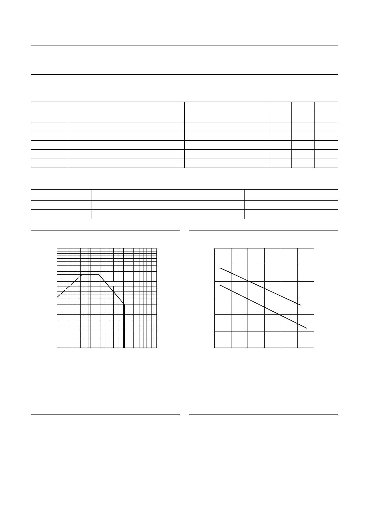
2
10
handbook, halfpage
I
D
(A)
10
(1) (2)
1
−1
10
110
(1) Current is this area may be limited by R
(2) Tmb = 25 °C.
Fig.2 DC SOAR.
2
10
V
DS(on)
DS
.
MRA906
(V)
300
handbook, halfpage
P
tot
(W)
200
100
3
10
0
0
(1) Short-time operation during mismatch.
(2) Continuous operation.
50
(1)
(2)
100 150
MGP089
Th (°C)
Fig.3 Power/temperature derating curves.
September 1992 3
Philips Semiconductors Product specification
HF/VHF power MOS transistor BLF177
CHARACTERISTICS
T
= 25 °C unless otherwise specified.
j
SYMBOL PARAMETER CONDITIONS MIN. TYP. MAX. UNIT
V
(BR)DSS
I
DSS
I
GSS
V
GS(th)
∆V
GS
g
fs
R
DS(on)
I
DSX
C
is
C
os
C
rs
drain-source breakdown voltage ID = 50 mA; VGS = 0 110 −−V
drain-source leakage current VGS = 0; VDS = 50 V −−2.5 mA
gate-source leakage current ±VGS = 20 V; VDS = 0 −−1µA
gate-source threshold voltage ID = 50 mA; VDS = 10 V 2 − 4.5 V
gate-source voltage difference of
ID = 50 mA; VDS = 10 V −−100 mV
matched pairs
forward transconductance ID = 5 A; VDS = 10 V 4.5 6.2 − S
drain-source on-state resistance ID = 5 A; VGS = 10 V − 0.2 0.3 Ω
on-state drain current VGS = 10 V; VDS = 10 V − 25 − A
input capacitance VGS = 0; VDS = 50 V; f = 1 MHz − 480 − pF
output capacitance VGS = 0; VDS = 50 V; f = 1 MHz − 190 − pF
feedback capacitance VGS = 0; VDS = 50 V; f = 1 MHz − 14 − pF
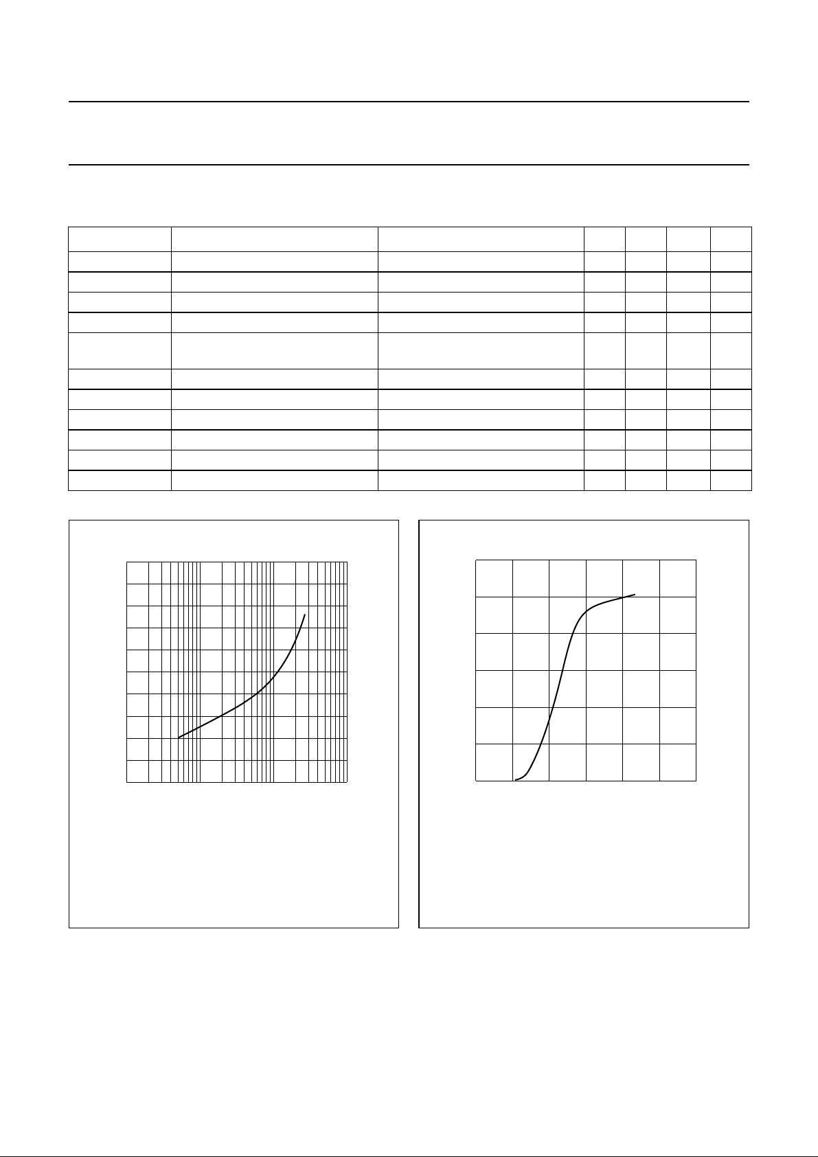
handbook, halfpage
0
T.C.
(mV/K)
−1
−2
−3
−4
−5
−2
VDS= 10 V; valid for Th= 25 to 70 °C.
−1
10
11010
ID (A)
Fig.4 Temperature coefficient of gate-source
voltage as a function of drain current, typical
values.
MGP090
30
handbook, halfpage
I
D
(A)
20
10
0
0
VDS= 10 V.
51015
MGP091
V
(V)
GS
Fig.5 Drain current as a function of gate-source
voltage, typical values.
September 1992 4
Philips Semiconductors Product specification
HF/VHF power MOS transistor BLF177
400
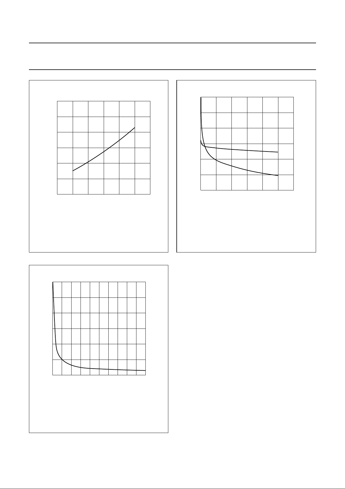
handbook, halfpage
R
DS(on)
(mΩ)
300
200
100
0
ID= 5 A; VGS= 10 V.
50 100 150
Tj (°C)
Fig.6 Drain-source on-state resistance as a
function of junction temperature, typical
values.
MGP092
C
is
C
os
MBK408
VDS (V)
1200
handbook, halfpage
C
(pF)
800
400
0
0
VGS= 0; f = 1 MHz.
20 40
Fig.7 Input and output capacitance as functions
of drain-source voltage, typical values.
60
300
handbook, halfpage
C
rs
(pF)
200
100
0
0
10 5020 30 40
VGS= 0; f = 1 MHz.
V
Fig.8 Feedback capacitance as a function of
drain-source voltage, typical values.
MGP093
DS
(V)
September 1992 5
 Loading...