

Page 1

BLF147
VHF power MOS transistor
Rev. 06 — 5 December 2006 Product data sheet
IMPORTANT NOTICE
Dear customer,
As from October 1st, 2006 Philips Semiconductors has a new trade name
- NXP Semiconductors, which will be used in future data sheets together with new contact
details.
In data sheets where the previous Philips references remain, please use the new links as
shown below.
http://www.philips.semiconductors.com use http://www.nxp.com
http://www.semiconductors.philips.com use http://www.nxp.com (Internet)
[email protected] use [email protected]
(email)
The copyright notice at the bottom of each page (or elsewhere in the document,
depending on the version)
- © Koninklijke Philips Electronics N.V. (year). All rights reserved is replaced with:
- © NXP B.V. (year). All rights reserved. If you have any questions related to the data sheet, please contact our nearest sales
office via e-mail or phone (details via [email protected]). Thank you for your
cooperation and understanding,
NXP Semiconductors
Page 2
NXP Semiconductors Product specification
Rev. 06 - 5 December 2006
2 of 15
VHF power MOS transistor BLF147
FEATURES
• High power gain
• Low intermodulation distortion
• Easy power control
• Good thermal stability
• Withstands full load mismatch.
APPLICATIONS
• Industrial and military applications in the HF/VHF
frequency range.
DESCRIPTION
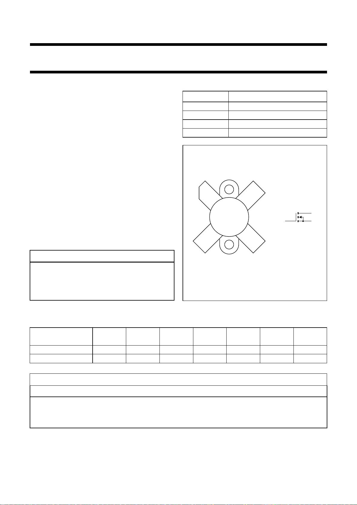
Silicon N-channel enhancement mode vertical D-MOS
transistor encapsulated in a 4-lead, SOT121B flange
packagewithaceramic cap.All leadsare isolatedfrom the
flange. A marking code, showing gate-source voltage
(VGS) information is provided for matched pair
applications. Refer to the “General” section of the
handbook for further information.
CAUTION
PINNING - SOT121B
PIN DESCRIPTION
1 drain
2 source
3 gate
4 source
handbook, halfpage
14
g
32
MAM267
d
s
This product issupplied in anti-static packing toprevent
damage caused by electrostatic discharge during
transport and handling. For further information, refer to
Philips specs.: SNW-EQ-608, SNW-FQ-302A, and
Fig.1 Simplified outline and symbol.
SNW-FQ-302B.
QUICK REFERENCE DATA
RF performance at Th = 25 °C in a common source test circuit.
MODE OF
OPERATION
f
(MHz)
V
(V)
DS
P
(W)
L
G
(dB)
p
η
D
(%)
d
3
(dB)
d
5
(dB)
SSB, class-AB 28 28 150 (PEP) >17 >35 <−30 <−30
CW, class-B 108 28 150 typ. 14 typ. 70 −−
WARNING
Product and environmental safety - toxic materials
This product contains beryllium oxide. The product is entirely safe provided that the BeO disc is not damaged.
All persons who handle, use or dispose of this product should be aware of its nature and of the necessary safety
precautions. Afteruse, dispose of as chemicalor special waste accordingto the regulations applying atthe location of
the user. It must never be thrown out with the general or domestic waste.
Page 3
NXP Semiconductors Product specification
Rev. 06 - 5 December 2006
3 of 15
VHF power MOS transistor BLF147
LIMITING VALUES
In accordance with the Absolute Maximum System (IEC 60134).
SYMBOL PARAMETER CONDITIONS MIN. MAX. UNIT
V
DS
V
GS
I
D
P
tot
T
stg
T
j
THERMAL CHARACTERISTICS
SYMBOL PARAMETER VALUE UNIT
R
th j-mb
R
th mb-h
drain-source voltage − 65 V
gate-source voltage −±20 V
drain current (DC) − 25 A
total power dissipation Tmb≤ 25 °C − 220 W
storage temperature −65 150 °C
junction temperature − 200 °C
thermal resistance from junction to mounting base 0.8 K/W
thermal resistance from mounting base to heatsink 0.2 K/W
2
10
handbook, halfpage
I
D
(A)
(1)
10
1
110
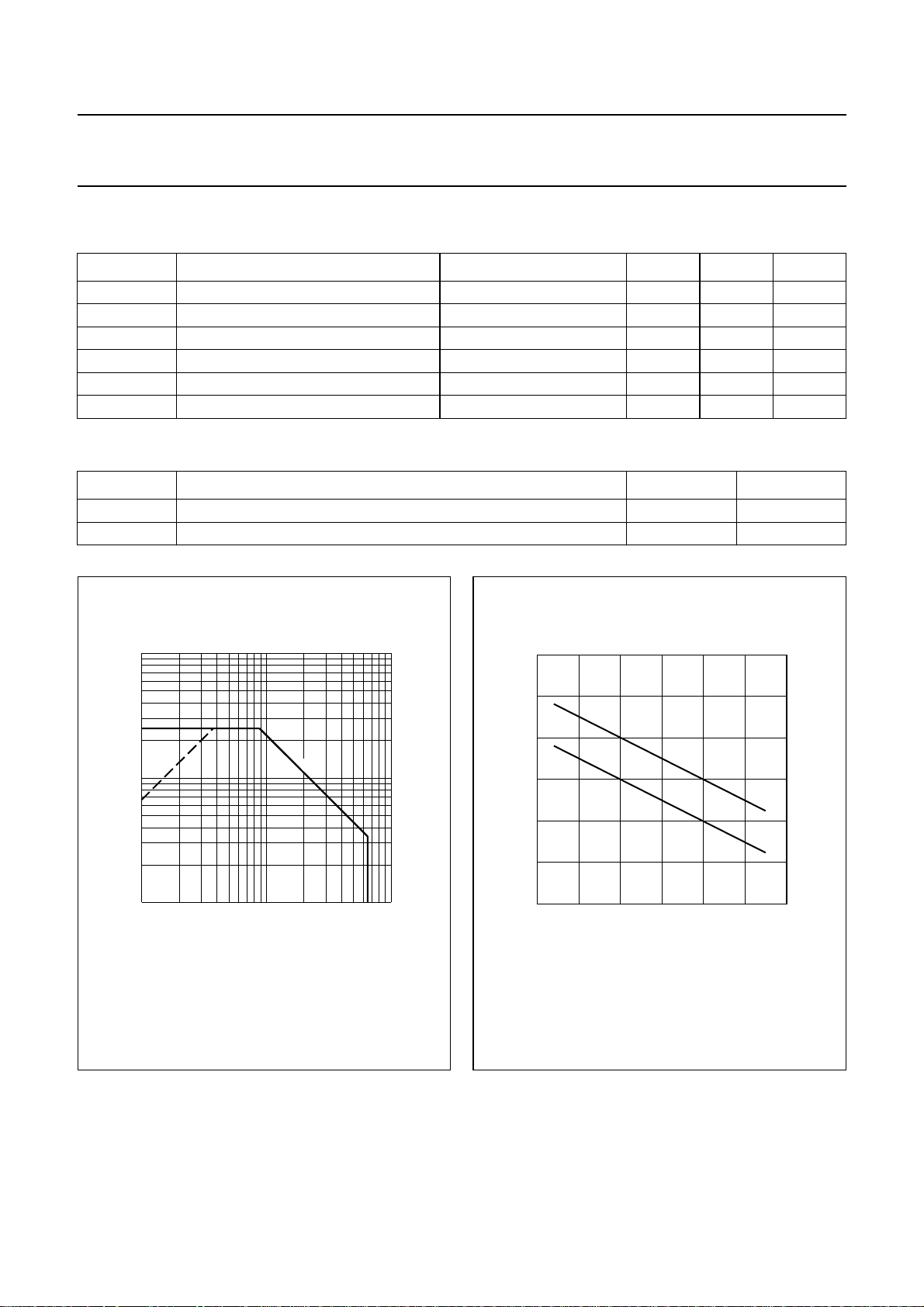
(1) Current is this area may be limited by R
(2) Tmb=25°C.
Fig.2 DC SOAR.
MRA904
(2)
2
V
(V)
DS
.
DSon
10
300
handbook, halfpage
P
tot
(W)
200
100
0
0
(1) Short-time operation during mismatch.
(2) Continuous operation.
(1)
(2)
50 100 150
Fig.3 Power derating curves.
MGP049
Th (°C)
Page 4
NXP Semiconductors Product specification
Rev. 06 - 5 December 2006
4 of 15
VHF power MOS transistor BLF147
CHARACTERISTICS
Tj = 25 °C unless otherwise specified.
SYMBOL PARAMETER CONDITIONS MIN. TYP. MAX. UNIT
V
(BR)DSS
I
DSS
I
GSS
V
GSth
∆V
GS
g
fs
R
DSon
I
DSX
C
is
C
os
C
rs
drain-source breakdown voltage ID= 100 mA; VGS=0 65 −−V
drain-source leakage current VGS= 0; VDS=28V −−5mA
gate-source leakage current VGS= ±20 V; VDS=0 −−1µA
gate-source threshold voltage ID= 200 mA; VDS=10V 2 − 4.5 V
gate-source voltage difference of
ID= 100 mA; VDS=10V −−100 mV
matched pairs
forward transconductance ID= 8 A; VDS=10V 5 7.5 − S
drain-source on-state resistance ID= 8 A; VGS=10V − 0.1 0.15 Ω
on-state drain current VGS= 10 V; VDS=10V − 37 − A
input capacitance VGS= 0; VDS=28V; f=1MHz − 450 − pF
output capacitance VGS= 0; VDS=28V; f=1MHz − 360 − pF
feedback capacitance VGS= 0; VDS=28V; f=1MHz − 55 − pF
VGS group indicator
GROUP
A 2.0 2.1 O 3.3 3.4
B 2.1 2.2 P 3.4 3.5
C 2.2 2.3 Q 3.5 3.6
D 2.3 2.4 R 3.6 3.7
E 2.4 2.5 S 3.7 3.8
F 2.5 2.6 T 3.8 3.9
G 2.6 2.7 U 3.9 4.0
H 2.7 2.8 V 4.0 4.1
J 2.8 2.9 W 4.1 4.2
K 2.9 3.0 X 4.2 4.3
L 3.0 3.1 Y 4.3 4.4
M 3.1 3.2 Z 4.4 4.5
N 3.2 3.3
LIMITS
(V)
GROUP
LIMITS
(V)
MIN. MAX. MIN. MAX.
Page 5
NXP Semiconductors Product specification
Rev. 06 - 5 December 2006
5 of 15
VHF power MOS transistor BLF147
handbook, halfpage
0
T.C.
(mV/K)
−1
−2
−3
−4
−5
−2
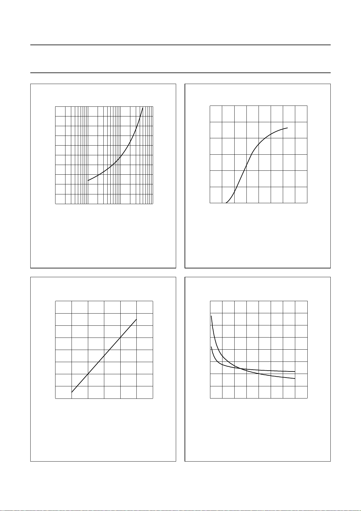
VDS= 28 V; valid for Th=25to70°C.
−1
10
11010
ID (A)
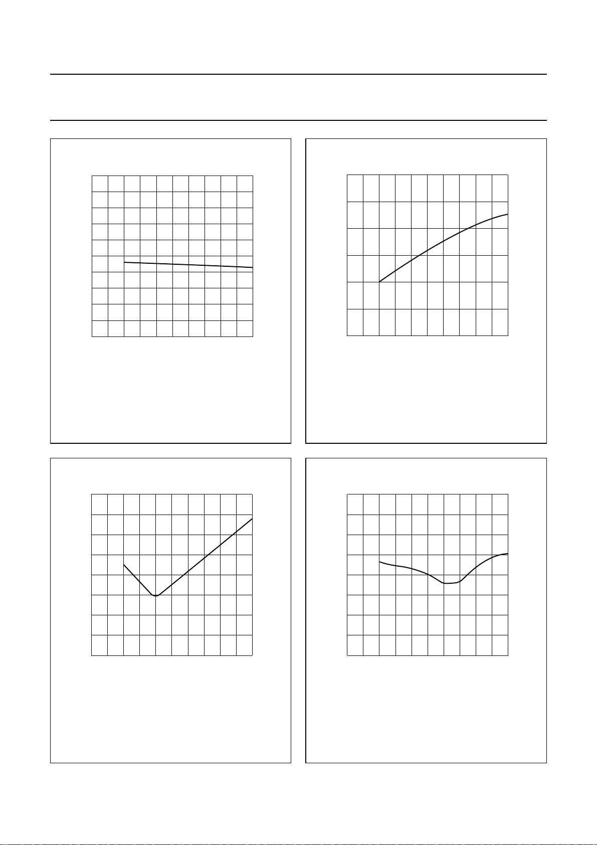
Fig.4 Temperature coefficient of gate-source
voltageas afunctionofdraincurrent; typical
values.
MGP050
V
GS
MGP051
(V)
60
handbook, halfpage
I
D
(A)
40
20
0
0
VDS=10V.
510 2015
Fig.5 Drain current as a function of gate-source
voltage; typical values.
170
handbook, halfpage
R
DSon
(mΩ)
150
130
110
90
0 50 100 150
ID= 8 A; VGS=10V.
Tj ( C)
Fig.6 Drain-source on-state resistance as a
function of junction temperature; typical
values.
MGP052
1400
handbook, halfpage
C
(pF)
1200
800
400
0
01020
VGS= 0; f = 1 MHz.
C
is
C
os
MRA903
30 40
V
(V)
DS
Fig.7 Input and output capacitance as functions
of drain-source voltage; typical values.
Page 6
NXP Semiconductors Product specification
Rev. 06 - 5 December 2006
6 of 15
VHF power MOS transistor BLF147
500
handbook, halfpage
C
rs
(pF)
400
300
200
100
0
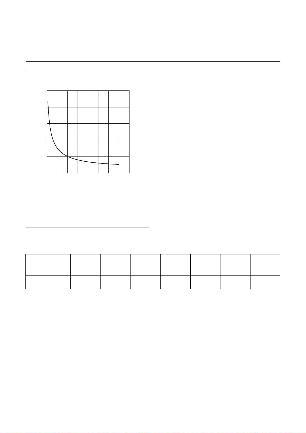
01020
VGS= 0; f = 1 MHz.
MRA902
30
40
V
(V)
DS
Fig.8 Feedback capacitance as a function of
drain-source voltage; typical values.
APPLICATION INFORMATION FOR CLASS-AB OPERATION
RF performance in SSB operation in a common source class-AB circuit.
Th=25°C; R
= 0.2 K/W; RGS= 9.8 Ω; f1= 28.000 MHz; f2= 28.001 MHz; unless otherwise specified.
th mb-h
P
(W)
L
f
(MHz)
V
(V)
DS
I
DQ
(A)
G
(dB)
20 to 150 (PEP) 28 28 1 >17
typ. 19
d
p
η
D
(%)
>35
typ. 40
3
(dB)
(note 2)
<−30
typ. −34
d
5
(dB)
(note 2)
<−30
typ. −40
Notes
1. Optimum load impedance: 2.1 + j0 Ω.
2. Maximum values at drive levels within the specified PEP values for either amplified tone. For the peak envelope
power the values should be decreased by 6 dB.
Ruggedness in class-AB operation
The BLF147 is capable of withstanding a load mismatch corresponding to VSWR = 50:1 through all phases under the
following conditions: V
= 28 V; f = 28 MHz at rated load power.
DS
Page 7
NXP Semiconductors Product specification
Rev. 06 - 5 December 2006
7 of 15
VHF power MOS transistor BLF147
30
handbook, halfpage
G
p
(dB)
20
10
0 200
Class-AB operation; VDS= 28 V; IDQ= 1 A;
= 9.8 Ω; f1= 28.000 MHz; f2= 28.001 MHz.
R
GS
100
PL (W) PEP
MGP053
Fig.9 Power gain as a function of load power;
typical values.
60
handbook, halfpage
η
D
(%)
40
20
0
0
Class-AB operation; VDS= 28 V; IDQ=1A;
= 9.8 Ω; f1= 28.000 MHz; f2= 28.001 MHz.
R
GS
100 200
PL (W) PEP
Fig.10 Efficiency as a function of load power;
typical values.
MGP054
−20
handbook, halfpage
d
3
(dB)
−30
−40
−50
−60
0
Class-AB operation; VDS= 28 V; IDQ=1A;
= 9.8 Ω; f1= 28.000 MHz; f2= 28.001 MHz.
R
GS
100 200
PL (W) PEP
MGP055
Fig.11 Third order intermodulation distortion as a
function of load power; typical values.
−20
handbook, halfpage
d
5
(dB)
−30
−40
−50
−60
0
Class-AB operation; VDS= 28 V; IDQ=1A;
= 9.8 Ω; f1= 28.000 MHz; f2= 28.001 MHz.
R
GS
100 200
PL (W) PEP
MGP056
Fig.12 Fifth order intermodulation distortion as a
function of load power; typical values.
Page 8
NXP Semiconductors Product specification
Rev. 06 - 5 December 2006
8 of 15
VHF power MOS transistor BLF147
handbook, full pagewidth
input
50 Ω
C1
C2
C3
C8
D.U.T.
L1
R3
R4
+V
G
L2
R2R1
C4
L3
C5
C9
L4
R5
L6L5
C7
C10
C12
C11
C14
C15
C13
output
50 Ω
L7
C6
f = 28 MHz.
+V
D
MGP057
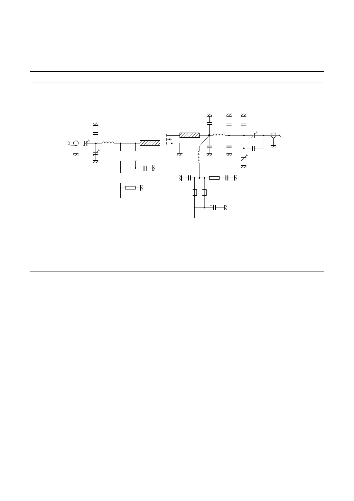
Fig.13 Test circuit for class-AB operation.
Page 9
NXP Semiconductors Product specification
Rev. 06 - 5 December 2006
9 of 15
VHF power MOS transistor BLF147
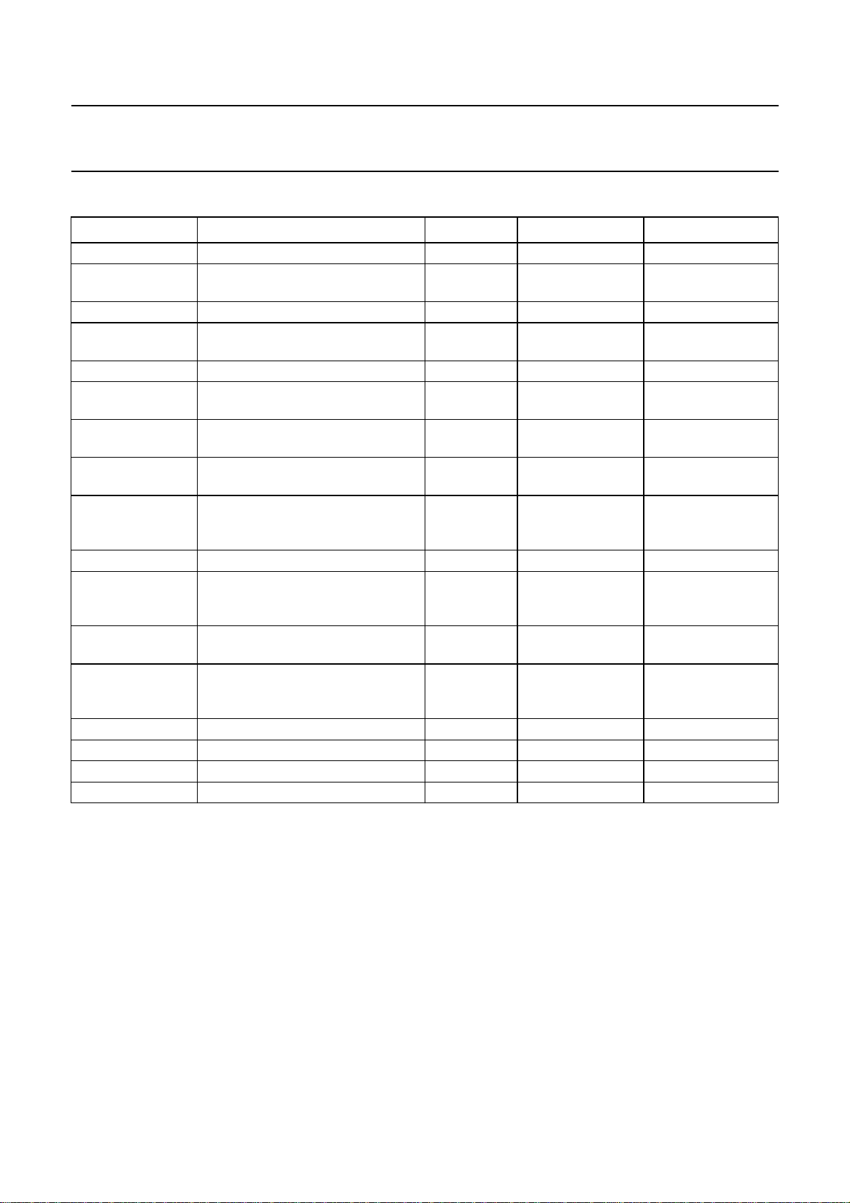
List of components (see Fig 13).
COMPONENT DESCRIPTION VALUE DIMENSIONS CATALOGUE NO.
C1, C3, C13, C14 film dielectric trimmer 7 to 100 pF 2222 809 07015
C2, C8, C9 multilayer ceramic chip capacitor;
note 1
C4, C5 multilayer ceramic chip capacitor 100 nF 2222 852 47104
C6 multilayer ceramic chip capacitorsin
parallel
C7 electrolytic capacitor 2.2 µF, 63 V
C10 multilayer ceramic chip capacitor;
note 1
C11, C12 multilayer ceramic chip capacitor;
note 1
C15 multilayer ceramic chip capacitor;
note 1
L1 6 turns enamelled 0.7 mm copper
wire
L2, L3 stripline; note 2 41.1 Ω length 13 × 6mm
L4 4 turns enamelled 1.5 mm copper
wire
L5, L6 grade 3B Ferroxcube wideband HF
choke
L7 3 turns enamelled 2.2 mm copper
wire
R1, R2 1 W metal film resistor 19.6 Ω 2322 153 51969
R3 0.4 W metal film resistor 10 kΩ 2322 151 71003
R4 0.4 W metal film resistor 1 MΩ 2322 151 71005
R5 1 W metal film resistor 10 Ω 2322 153 51009
75 pF
3 × 100 nF 2222 852 47104
100 pF
150 pF
240 pF
145 nH length 5 mm;
int. dia. 6 mm;
leads 2 × 5mm
148 nH length 8 mm;
int. dia. 10 mm;
leads 2 × 5mm
4312 020 36642
79 nH length 8 mm;
int. dia. 8 mm;
leads 2 × 5mm
Notes
1. American Technical Ceramics (ATC) capacitor, type 100B or other capacitor of the same quality.
2. The striplines are on a double copper-clad printed circuit board, with PTFE fibre-glass dielectric (ε
thickness 1.6 mm.
= 2.2),
r
Page 10
NXP Semiconductors Product specification
Rev. 06 - 5 December 2006
10 of 15
VHF power MOS transistor BLF147
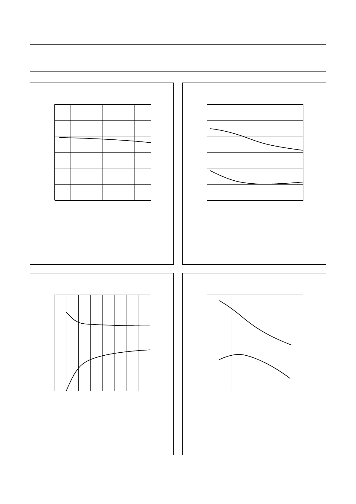
30
handbook, halfpage
G
P
(dB)
20
10
0
0
Class-AB operation; VDS= 28 V; IDQ=1A;
= 6.25 Ω; PL= 150 W (PEP); RL= 2.1 Ω.
R
GS
10 20 30
f (MHz)
Fig.14 Power gain as a function of frequency;
typical values.
MGP058
f (MHz)
MGP059
r
i
x
i
10
handbook, halfpage
Z
i
(Ω)
5
0
−5
0
Class-AB operation; VDS= 28 V; IDQ=1A;
= 6.25 Ω; PL= 150 W (PEP); RL= 2.1 Ω.
R
GS
10 20
Fig.15 Input impedance as a functionof frequency
(series components); typical values.
30
150
MGP061
f (MHz)
r
i
x
i
handbook, halfpage
4
Z
i
(Ω)
2
0
−2
−4
0 50 100 200
Class-B operation; VDS=28V;IDQ= 0.2 A;
=15Ω; PL= 150 W.
R
GS
Fig.16 Input impedance as a functionof frequency
(series components); typical values.
L
L
150
MGP062
f (MHz)
handbook, halfpage
3
Z
L
(Ω)
2
1
0
−1
0 50 100 200
Class-B operation; VDS= 28 V; IDQ= 0.2 A;
=15Ω; PL= 150 W.
R
GS
R
X
Fig.17 Load impedance as a functionof frequency
(series components); typical values.
Page 11
NXP Semiconductors Product specification
Rev. 06 - 5 December 2006
11 of 15
VHF power MOS transistor BLF147
30
handbook, halfpage
G
p
(dB)
20
10
0
0
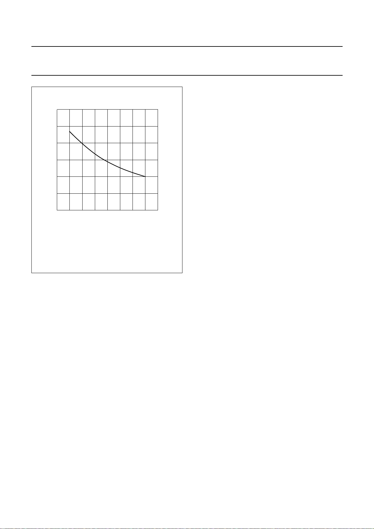
Class-B operation; VDS= 28 V; IDQ= 0.2 A;
=15Ω; PL= 150 W.
R
GS
50 100 200150
f (MHz)
Fig.18 Power gain as a function of frequency;
typical values.
MGP060
Page 12
NXP Semiconductors Product specification
Rev. 06 - 5 December 2006
12 of 15
VHF power MOS transistor BLF147
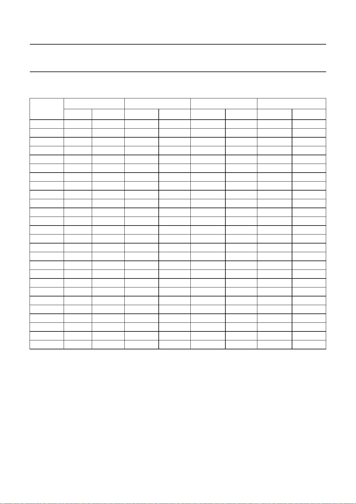
BLF147 scattering parameters
VDS= 28 V; ID= 1000 mA; note 1
f (MHz)
s
11
s
21
s
12
s
22
|s11| ∠Φ |s21| ∠Φ |s12| ∠Φ |s22| ∠Φ
5 0.91 −170.00 23.90 93.40 0.01 5.80 0.88 −171.20
10 0.91 −174.60 12.25 89.40 0.01 3.60 0.89 −177.20
20 0.92 −177.40 5.94 81.00 0.01 5.40 0.83 −179.60
30 0.92 −178.40 3.87 79.10 0.01 8.90 0.86 −178.90
40 0.92 −178.80 2.84 75.70 0.01 12.00 0.85 −178.60
50 0.92 −178.80 2.26 73.30 0.01 16.90 0.87 −176.90
60 0.92 −179.00 1.88 69.80 0.01 20.30 0.90 −177.30
70 0.93 −179.20 1.58 66.20 0.01 24.00 0.90 −178.10
80 0.93 −179.60 1.36 63.20 0.01 28.80 0.90 −178.40
90 0.93 −179.70 1.19 60.40 0.01 34.20 0.90 −178.60
100 0.94 −179.70 1.05 57.00 0.01 39.30 0.90 −179.40
125 0.95 179.50 0.77 49.30 0.01 52.30 0.88 179.20
150 0.95 179.00 0.60 45.80 0.01 64.90 0.91 −179.50
175 0.96 178.10 0.49 41.50 0.02 72.40 0.95 179.80
200 0.96 177.50 0.40 36.80 0.02 75.80 0.94 177.70
250 0.97 175.80 0.28 33.20 0.03 82.30 0.95 176.20
300 0.98 174.20 0.22 30.10 0.03 83.00 0.96 173.60
350 0.98 172.70 0.17 31.00 0.04 85.00 0.97 171.90
400 0.98 171.10 0.14 32.40 0.05 84.90 0.97 169.50
450 0.98 169.50 0.12 36.10 0.05 85.90 0.97 167.70
500 0.98 167.90 0.11 39.90 0.06 84.30 0.98 165.50
600 0.98 164.80 0.10 50.20 0.07 83.20 0.97 161.50
700 0.98 161.60 0.10 57.90 0.09 81.70 0.97 157.50
800 0.98 158.20 0.11 63.70 0.10 81.00 0.97 153.50
900 0.97 154.60 0.13 67.20 0.12 79.50 0.97 149.30
1000 0.97 151.10 0.14 70.20 0.14 78.80 0.96 144.90
Note
1. For more extensive S-parameters see internet:
http://www.semiconductors.philips.com/markets/communications/wirelesscommunications/broadcast.
Page 13
NXP Semiconductors Product specification
Rev. 06 - 5 December 2006
13 of 15
VHF power MOS transistor BLF147
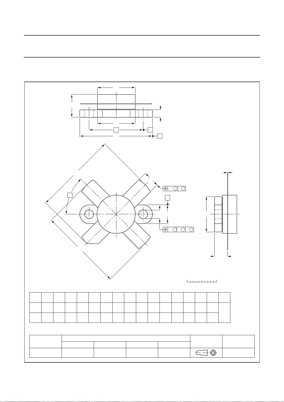
PACKAGE OUTLINE
Flanged ceramic package; 2 mounting holes; 4 leads SOT121B
D
A
F
D
1
q
U
1
C
B
H
b
43
α
p
12
H
DIMENSIONS (millimetre dimensions are derived from the original inch dimensions)
UNIT
mm
inches
A
7.27
6.17
0.286
0.243
5.82
5.56
0.229
0.219
c
0.16
0.10
0.006
0.004
Db
12.86
12.59
0.506
0.496
D
12.83
12.57
0.505
0.495
F
1
2.67
28.45
2.41
25.52
1.120
0.105
0.095
1.005
0.130
0.120
pH
3.30
3.05
Q
4.45
3.91
0.175
0.154
q
18.42
0.725
w
MM
C
2
A
U
2
w
MMM
AB
1
0 5 10 mm
U
U
1
24.90
24.63
0.98
0.97
6.48
6.22
0.255
0.245
3
2
12.32
12.06
0.485
0.475
U
scale
w1w
0.25
0.01
c
3
Q
αU
2
0.51
45°
0.02
OUTLINE
VERSION
SOT121B 99-03-29
REFERENCES
IEC JEDEC EIAJ
EUROPEAN
PROJECTION
ISSUE DATE
Page 14

NXP Semiconductors
Rev. 06 - 5 December 2006
14 of 15
Legal information
Data sheet status
BLF147
VHF power MOS transistor
Document status
Objective [short] data sheet Development This document contains data from the objective specification for product development.
Preliminary [short] data sheet Qualification This document contains data from the preliminary specification.
Product [short] data sheet Production This document contains the product specification.
[1] Please consult the most recently issued document before initiating or completing a design.
[2] The term ‘short data sheet’ is explained in section “Definitions”.
[3] The product status of device(s)described in this document mayhavechangedsince this document was published andmaydifferin case of multiple devices. The latestproduct status
information is available on the Internet at URL
[1][2]
Product status
Definitions
Draft — The document is a draft version only. The content is still under
internal review and subject to formal approval, which may result in
modifications or additions. NXP Semiconductors does not give any
representations or warranties as to the accuracy or completeness of
information included hereinand shall have no liabilityfor the consequences of
use of such information.
Short data sheet — A short data sheet is an extract from a full data sheet
with the sameproduct type number(s) andtitle. A shortdata sheet is intended
for quick reference onlyand should not be relied upon to contain detailed and
full information. For detailed and full information see the relevant full data
sheet, which is available on request via the local NXP Semiconductors sales
office. In case of any inconsistency or conflict with the short data sheet, the
full data sheet shall prevail.
Disclaimers
General — Information in this document is believed to be accurate and
reliable. However, NXP Semiconductors does notgive any representations or
warranties, expressed or implied,as to the accuracy orcompleteness of such
information and shall have no liability for the consequences of use of such
information.
Right to make changes — NXP Semiconductors reservesthe right to make
changes to information published in this document, including without
limitation specifications and product descriptions, at any time and without
notice. This documentsupersedes and replaces all information supplied prior
to the publication hereof.
Suitability for use — NXP Semiconductors products are not designed,
authorized or warranted to be suitable for use in medical, military, aircraft,
space or life support equipment, nor in applications where failure or
[3]
http://www.nxp.com.
Definition
malfunction of a NXPSemiconductors product canreasonablybe expected to
result in personal injury, death or severe property or environmental damage.
NXP Semiconductors accepts no liability for inclusion and/or use of NXP
Semiconductors products in such equipment or applications and therefore
such inclusion and/or use is at the customer’s own risk.
Applications — Applications that are described herein for any of these
products are for illustrative purposes only. NXP Semiconductors makes no
representation or warranty that such applications will be suitable for the
specified use without further testing or modification.
Limiting values — Stress above one or more limiting values (as defined in
the Absolute MaximumRatings System of IEC 60134)may cause permanent
damage to thedevice.Limiting values arestress ratings onlyand operation of
the device at these or any other conditions above those given in the
Characteristics sections of this document is not implied. Exposure to limiting
values for extended periods may affect device reliability.
Terms and conditions of sale — NXP Semiconductors products are sold
subject to the general terms and conditions of commercial sale, as published
http://www.nxp.com/profile/terms, including those pertaining to warranty,
at
intellectual property rights infringement and limitation of liability, unless
explicitly otherwise agreed to in writing by NXP Semiconductors. In case of
any inconsistency or conflict between information in this document and such
terms and conditions, the latter will prevail.
No offer to sell or license — Nothing in this document may be interpreted
or construed as an offer to sell products that is open for acceptance or the
grant, conveyance or implication of anylicense under any copyrights, patents
or other industrial or intellectual property rights.
Trademarks
Notice: All referenced brands,productnames, service namesandtrademarks
are the property of their respective owners.
Contact information
For additional information, please visit: http://www.nxp.com
For sales office addresses, send an email to: [email protected]
Page 15

NXP Semiconductors
Rev. 06 - 5 December 2006
15 of 15
BLF147
VHF power MOS transistor
Revision history
Revision history
Document ID Release date Data sheet status Change notice Supersedes
BLF147_6 20061205 Product data sheet - BLF147_5
Modifications:
BLF147_5 20061108 Product data sheet - BLF147_4
BLF147_4
(9397 750 11593)
BLF147_3
(9397 750 08411)
BLF147_CNV_2
(9397 750 xxxxx)
• Correction made to page 9 “List of components”
20030901 Product specification - BLF147_3
20010523 Product specification - BLF147_CNV_2
19971215 Product specification - -
Please be aware that important notices concerning this document and the product(s)
described herein, have been included in section ‘Legal information’.
© NXP B.V. 2006. All rights reserved.
For more information, please visit: http://www.nxp.com
For sales office addresses, please send an email to: [email protected]
Date of release: 5 December 2006
Document identifier: BLF147_6
 Loading...