

Philips BLF1048 Datasheet

DISCRETE SEMICONDUCTORS
DATA SH EET
ook, halfpage
M3D379
BLF1048
UHF power LDMOS transistor
Preliminary specification
Supersedes data of 1999 July 01
2000 Feb 02
Philips Semiconductors Preliminary specification
UHF power LDMOS transistor BLF1048
FEATURES
• High power gain
• Easy power control
• Excellent ruggedness
• Source on underside eliminates DC isolators, reducing
common mode inductance
• Designed for broadband operation (HF to 1 GHz).
APPLICATIONS
• Communication transmitter applications in the UHF
frequency range.
DESCRIPTION
Silicon N-channel enhancement mode lateral D-MOS
transistor encapsulated in a 2-lead flange package
(SOT502A) with a ceramic cap. The common source is
connected to the mounting flange.
QUICK REFERENCE DATA
RF performance at Th=25°C in a common source test circuit.
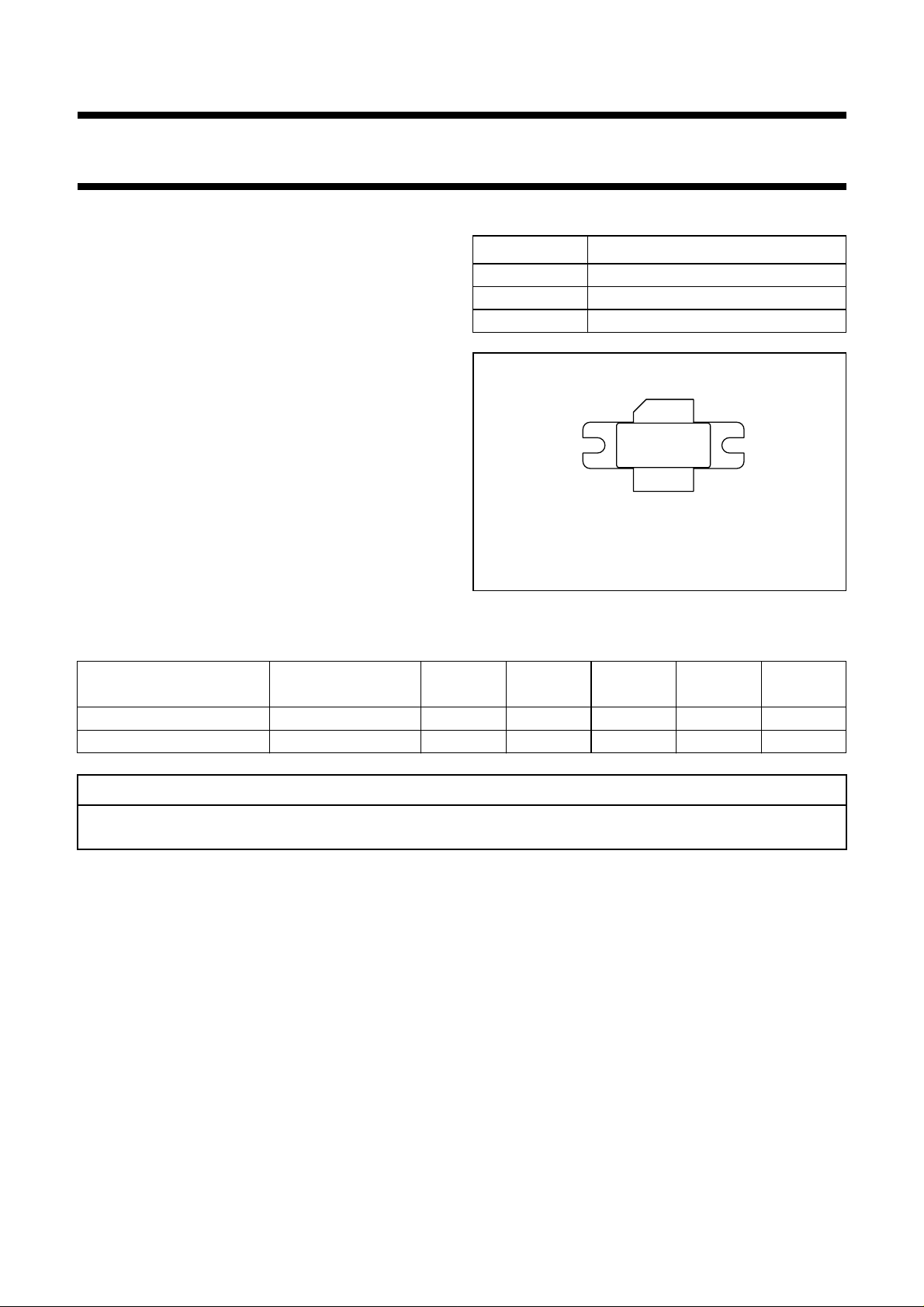
PINNING - SOT502A
PIN DESCRIPTION
1 drain
2 gate
3 source, connected to flange
handbook, halfpage
Top view
1
2
Fig.1 Simplified outline.
3
MBK394
MODE OF OPERATION
CW, class-AB (2-tone) f
f
(MHz)
= 960; f2= 960.1 26 90 (PEP) >14 >35 ≤−26
1
V
(V)
DS
P
(W)
L
G
(dB)
p
η
D
(%)
d
im
(dBc)
CW, class-AB (1-tone) 960 26 90 >14 >45 −
CAUTION
This product is supplied in anti-static packing to prevent damage caused by electrostatic discharge during transport
and handling. For further information, refer to Philips specs.: SNW-EQ-608, SNW-FQ-302A and SNW-FQ-302B.
2000 Feb 02 2
Philips Semiconductors Preliminary specification
UHF power LDMOS transistor BLF1048
LIMITING VALUES
In accordance with the Absolute Maximum Rating System (IEC 134).
SYMBOL PARAMETER MIN. MAX. UNIT
V
DS
V
GS
I
D
T
stg
T
j
THERMAL CHARACTERISTICS
SYMBOL PARAMETER CONDITIONS VALUE UNIT
R
th j-h
Note
1. Determined under specified RF operating conditions, based on maximum peak junction temperature.
drain-source voltage − 65 V
gate-source voltage −±20 V
drain current (DC) − 9A
storage temperature −65 +150 °C
junction temperature − 200 °C
thermal resistance from junction to heatsink Th=25°C; P
= 100 W;
tot
1.15 K/W
note 1
CHARACTERISTICS
=25°C unless otherwise specified.
T
j
SYMBOL PARAMETER CONDITIONS MIN. TYP. MAX. UNIT
V
(BR)DSS
V
GSth
I
DSS
I
DSX
I
GSS
g
fs
R
DSon
C
is
C
os
C
rs
drain-source breakdown voltage VGS= 0; ID= 1.4 mA 65 −−V
gate-source threshold voltage VDS= 10 V; ID= 140 mA 4 − 5V
drain-source leakage current VGS= 0; VDS=26V −−10 µA
drain cut-off current VGS=V
+9V; VDS=10V 25 −−A
GSth
gate leakage current VGS= ±20 V; VDS=0 −−250 nA
forward transconductance VDS= 10 V; ID=7A − 4 − S
drain-source on-state resistance VGS=V
+9V; ID=7A − 150 − mΩ
GSth
input capacitance VGS= 0; VDS= 26 V; f = 1 MHz − 92 − pF
output capacitance VGS= 0; VDS= 26 V; f = 1 MHz − 74 − pF
feedback capacitance VGS= 0; VDS= 26 V; f = 1 MHz − 3 − pF
APPLICATION INFORMATION
RF performance in a common source class-AB circuit. T
MODE OF OPERATION
CW, class-AB (2-tone) f
1
f
(MHz)
= 960; f2= 960.1 26 90 (PEP) >14 >35 ≤−26
=25°C; R
h
V
DS
(V)
= 1.15 K/W, unless otherwise specified.
th j-h
P
(W)
L
G
(dB)
p
η
D
(%)
d
(dBc)
CW, class-AB (1-tone) 960 26 90 >14 >45 −
im
Ruggedness in class-AB operation
The BLF1048is capable of withstanding a load mismatch corresponding to VSWR = 10 : 1 through all phases under the
following conditions: V
= 26 V; f = 960 MHz at rated load power.
DS
2000 Feb 02 3
 Loading...