

M3D379
查询BLF0810-90供应商
DISCRETE SEMICONDUCTORS
DATA SHEET
M3D461
BLF0810-90; BLF0810S-90
Base station LDMOS transistors
Preliminary specification 2002 Mar 18

Philips Semiconductors Preliminary specification
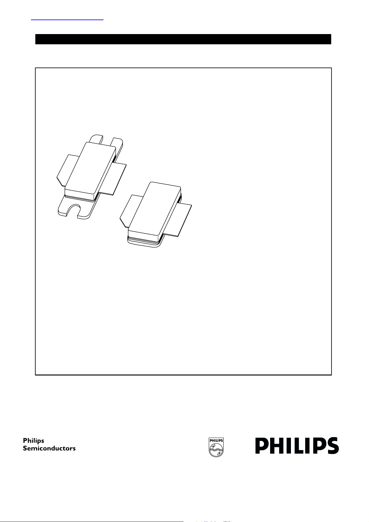
handbook, halfpage
Top view MBK394
1
2
3
Fig.1 Simplified outline SOT502A (BLF0810-90)
5
Base station LDMOS transistors BLF0810-90; BLF0810S-90
FEATURES
• High power gain
• Easy power control
• Excellent ruggedness
• Source on underside eliminates DC isolators, reducing
DESCRIPTION
Silicon N-channel enhancement mode lateral D-MOS
transistors encapsulated in a 2-lead flange package
(BLF0810-90) with a ceramic cap or in a 2-lead earless
package (BLF0810S-90). The common source is
connected to the flange.
common mode inductance
• Designed for broadband operation (750 MHz to 1 GHz).
Typical CDMA IS95 performance at standard settings at a
supply voltage of 27 V and I
APPLICATIONS
• Common source class-AB operation in CDMA
applications in the 750 to 960 MHz frequency range.
P
=18W
L
G
=16dB
P
η =26%
ACPR <−45 dBc at 750 kHz and BW = 30 kHz
ACPR <−63 dBc at 1.98 MHz and BW = 30 kHz
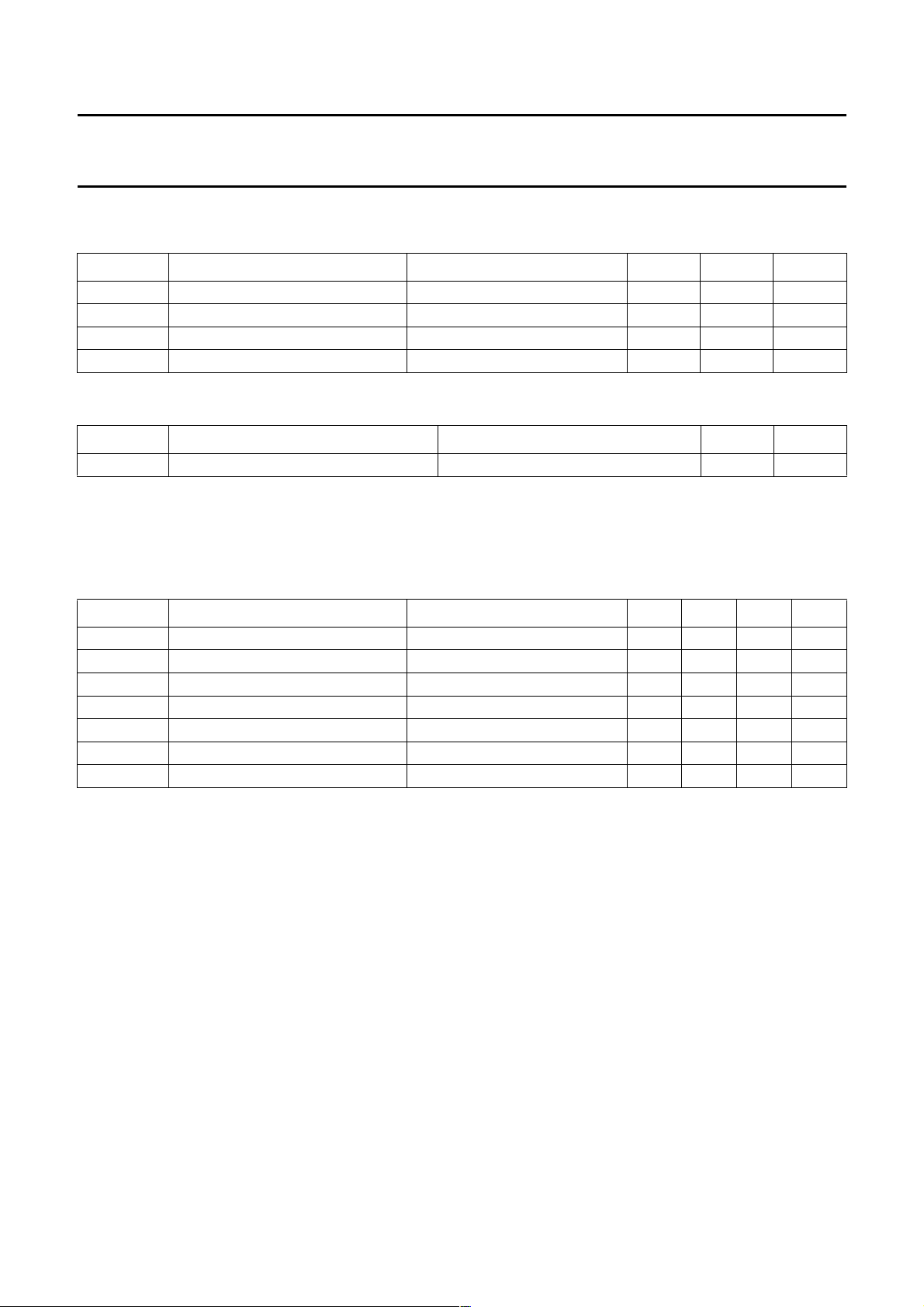
PINNING - SOT502A PINNING - SOT502B
PIN DESCRIPTION
1drain
2 gate
3 source; connected to flange
PIN DESCRIPTION
1drain
2
3 source; connected to flange
gate
=500mA
DQ
1
3
2
Top view
MBL10
Fig.2 Simplified outline SOT502B (BLF0810S-90)
QUICK REFERENCE DATA
2-tone performance at T
MODE OF OPERATION
=25°C in a common source test circuit.
h
f
(MHz)
V
(V)
DS
P
PEP
L
(W)
G
(dB)
p
η
D
(%)
d
3
(dBc)
Class-AB 881.4 - 881.6 27 60 typ. 16.5 typ. 35 typ. −30
MODE OF OPERATION
(1)
CDMA
f
(MHz)
881.5 27 18 typ. 16 typ. 26
V
(V)
DS
P
avg
L
(W)
G
(dB)
p
η
D
(%)
ACPR
(dB)
typ. −46
typ. −63
Note
1. IS95 CDMA (pilot, Paging, Sync, and Trafic Codes 8 trough 13)
2. ACPR 750 kHz at BW = 30 kHz
3. ACPR 1.98 MHz at BW = 30 kHz.
(2)
(3)
2002 Mar 18 2
Philips Semiconductors Preliminary specification
Base station LDMOS transistors BLF0810-90; BLF0810S-90
LIMITING VALUES
In accordance with the Absolute Maximum Rating System (IEC 60134).
SYMBOL PARAMETER CONDITIONS MIN. MAX. UNIT
V
DS
V
GS
T
stg
T
j
THERMAL CHARACTERISTICS
SYMBOL PARAMETER CONDITIONS VALUE UNIT
R
th j-c
Note
1. Thermal resistance is determined under RF operating conditions.
drain-source voltage − 75 V
gate-source voltage −±15 V
storage temperature −65 150 °C
junction temperature − 200 °C
thermal resistance from junction to case Th=25°C, PL= 18 W avg, note 1 <0.75 K/W
CHARACTERISTICS
T
=25°C unless otherwise specified.
j
SYMBOL PARAMETER CONDITIONS MIN. TYP. MAX. UNIT
V
(BR)DSS
V
GSth
I
DSS
I
DSX
I
GSS
g
fs
R
DSon
drain-source breakdown voltage VGS=0; ID=3mA 75 −−V
gate-source threshold voltage VDS=10V; ID= 300 mA 4 − 5V
drain-source leakage current VGS=0; VDS=36V −−1 µA
on-state drain current VGS=V
+9V; VDS=10V 28 −−A
GS(th)
gate leakage current VGS= ±20 V; VDS=0 −−1 µA
forward transconductance VDS=10V; ID=10A − 4.8 − S
drain-source on-state resistance VGS=9V; ID=10A − 120 − mΩ
2002 Mar 18 3
Philips Semiconductors Preliminary specification
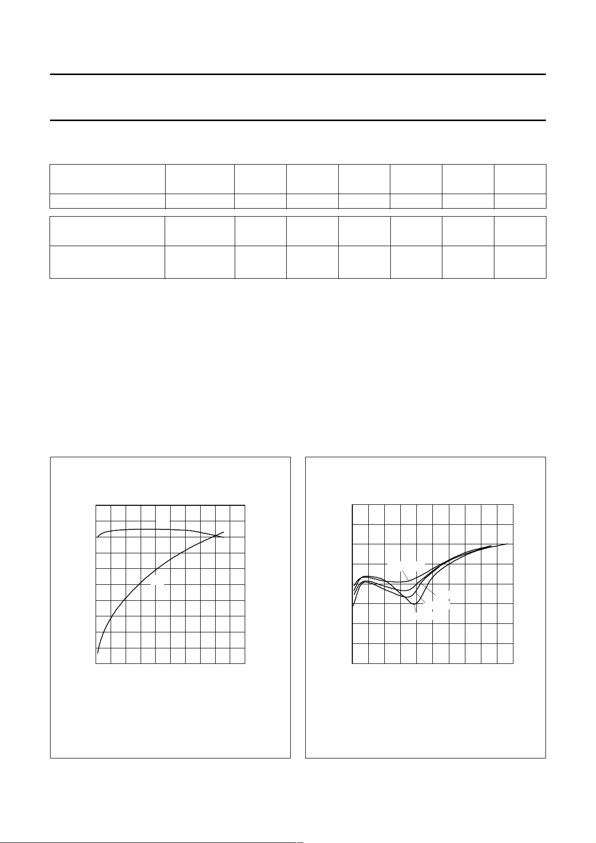
Fig.3 Power gain and efficiency as functions of
peak envelope load power, typical values.
VDS=27V; IDQ= 500 mA; f1=881.4MHz; f2=881.6MHz.
Base station LDMOS transistors BLF0810-90; BLF0810S-90
APPLICATION INFORMATION
RF performance in a common source-AB circuit; T
=25°C.
h
MODE OF OPERATION
f
(MHz)
V
(V)
DS
I
DQ
(mA)
P
PEP
L
(W)
G
(dB)
p
η
D
(%)
d
3
(dBc)
Class-AB 881.4 - 881.6 27 500 60 >16 >35 <−30
MODE OF OPERATION
(1)
CDMA
f
(MHz)
V
(V)
DS
I
DQ
(mA)
P
avg
L
(W)
881.5 27 500 >16 >15 >26
G
(dB)
p
η
D
(%)
ACPR
(dB)
<−46
<−63
Note
1. IS95 CDMA (pilot, Paging, Sync, and Trafic Codes 8 trough 13)
2. ACPR 750 kHz at BW = 30 kHz
3. ACPR 1.98 MHz at BW = 30 kHz.
Ruggedness in class-AB operation
The BLF0810-90 and BLF0810S-90 are capable of withstanding a load mismatch corresponding to VSWR = 10 : 1
through all phases at V
=27V; PL= 60 W (PEP).
DS
(2)
(3)
20
G
P
(dB)
16
12
8
4
0
0 20406080100
G
P
η
D
2002 Mar 18 4
(PEP) (W)
P
L
50
40
30
20
10
0
η
(%)
0
d
D
3
(dBc)
-20
IDQ=400mA
-40
450mA
500mA
-60
-80
0 20406080100
VDS=27V; f1= 881.4 MHz; f2=881.6MHz.
600mA
P
(PEP) (W)
L
Fig.4 Intermodulation distortion as a function of
peak envelope load power, typical values.
 Loading...