

Philips BGY925-5 Datasheet
DATA SHEET
Preliminary specification 1999 Jul 30
DISCRETE SEMICONDUCTORS
BGY925/5
UHF amplifier module
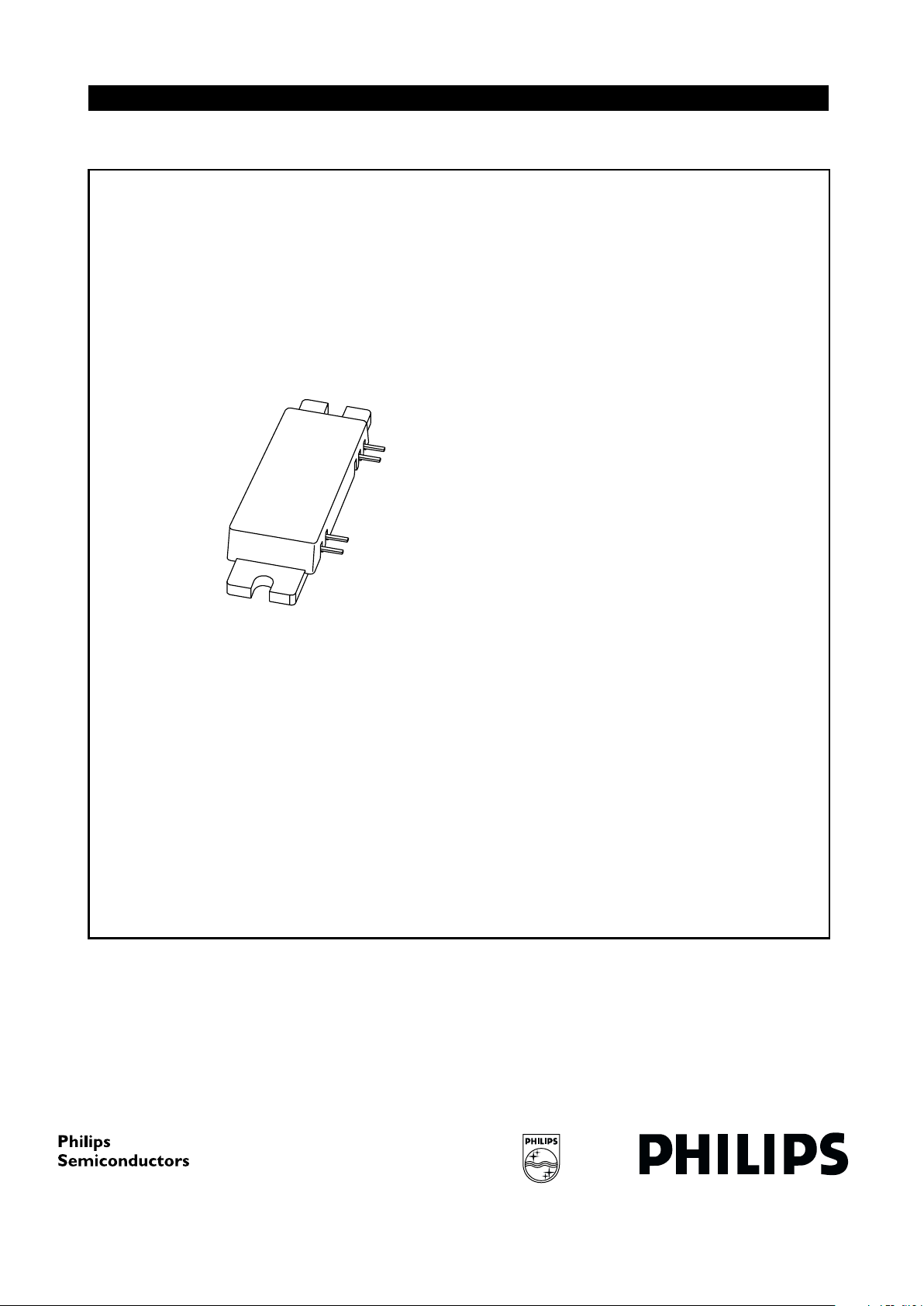
andbook, halfpage
M3D167

1999 Jul 30 2
Philips Semiconductors Preliminary specification
UHF amplifier module BGY925/5
FEATURES
• 26 V nominal supply voltage
• 23 W output power into a load of 50 Ω with an RF drive
power of 36 mW.
APPLICATIONS
• Base station transmitting equipment operating in the
920 to 960 MHz frequency range.
DESCRIPTION
The BGY925A is a three-stage UHF amplifier module in a
SOT365A package. It consists of one NPN silicon planar
transistor die and two silicon MOSFET dies mounted on a
metallized ceramic AlN substrate, together with matching
and bias circuitry.
PINNING - SOT365A
PIN DESCRIPTION
1 RF input
2V
S1
3V
S2
4 RF output
Flange ground
Fig.1 Simplified outline.
dbook, halfpage
MSA447
2134
QUICK REFERENCE DATA
RF performance at T
mb
=25°C.
Note
1. At P
L
=16W.
MODE OF
OPERATION
f
(MHz)
V
S1
(V)
V
S2
(V)
P
L
(W)
G
p
(dB)
η
(%)
(note 1)
Z
S
, Z
L
(Ω)
CW 920to960 5 26 23 ≥28 ≥30 50

1999 Jul 30 3
Philips Semiconductors Preliminary specification
UHF amplifier module BGY925/5
LIMITING VALUES
In accordance with the Absolute Maximum Rating System (IEC 134).
CHARACTERISTICS
Z
S=ZL
=50Ω; PL=23W; VS1=5V; VS2=26V; Tmb=25°C; unless otherwise specified.
SYMBOL PARAMETER MIN. MAX. UNIT
V
S1
DC supply voltage − 28 V
V
S2
DC supply voltage − 28 V
P
D
input drive power − 80 mW
P
L
load power − 32 W
T
stg
storage temperature −30 +100 °C
T
mb
operating mounting-base temperature −10 +90 °C
SYMBOL PARAMETER CONDITIONS MIN. TYP. MAX. UNIT
f frequency range 920 − 960 MHz
I
S1
supply current − 50 − mA
I
S2
supply current PD< −60 dBm − 500 − mA
P
L
load power 23 −−W
G
p
power gain 160 mW ≤ PL≤ 23W 283032dB
out of band gain P
L
= 160 mW; f <920 MHz; f >960 MHz −−1.5 dB
∆G
p
in-band gain variation f = 920 MHz - 960 MHz −−1.5 dB
|G
P1-GP2
| gain expansion GP1 at PL= 160 mW; GP2 at PL=5W −−±0.75 dB
η efficiency P
L
=16W 30 −−%
H
2
second harmonic PL=16W −−−35 dBc
H
3
third harmonic PL=16W −−−40 dBc
VSWR
in
input VSWR −−2:1
stability VSWR ≤ 3 : 1 through all phases;
V
S2
=26to27V; PL=23W
−−−60 dBc
reverse intermodulation P
carrier
=16W; P
interference
=1.6µW;
f
i=fc
± 600 kHz
−−80 − dBc
direct intermodulation P
carrier
=16W; P
interference
= 1.6 mW;
f
i=fc
+ 270 kHz
−−55 − dBc
NF noise figure 8dBc
B AM bandwidth corner frequency = 3 dB;
P
carrier
= 16 W; modulation = 20%
2 −−MHz
ruggedness VSWR ≤ 5 : 1 through all phases;
V
S2
=26V; PL=23W
no degradation
 Loading...