

Philips BGY888 Datasheet
DISCRETE SEMICONDUCTORS
DATA SH EET
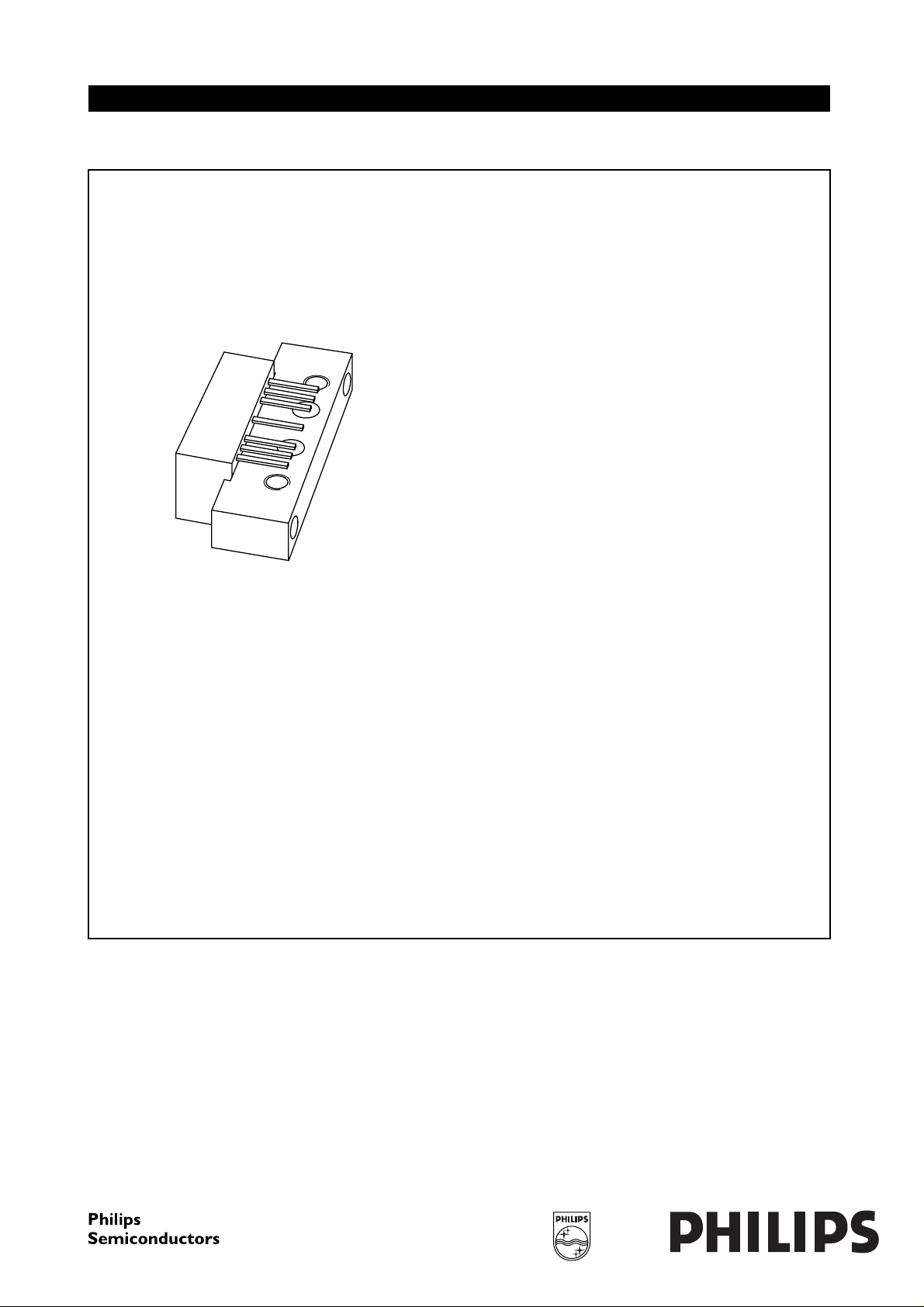
ook, halfpage
M3D252
BGY888
CATV amplifier module
Product specification
Supersedes data of 1997 Apr 10
1999 Mar 30
Philips Semiconductors Product specification
CATV amplifier module BGY888
FEATURES
• Excellent linearity
• Extremely low noise
• High gain
• Excellent return loss properties.
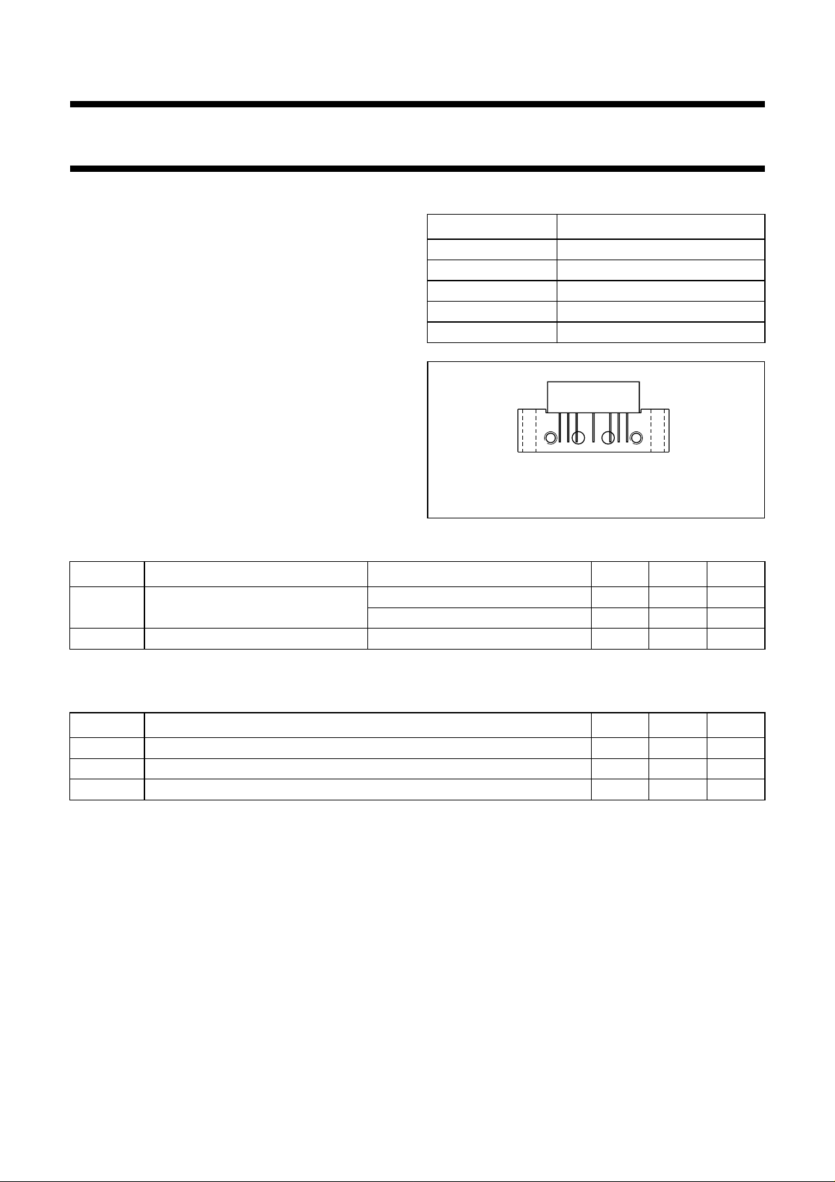
PINNING SOT115J
PIN DESCRIPTION
1 input
2, 3 common
5+V
B
7, 8 common
APPLICATIONS
9 output
• Single module line extender in CATV systems operating
over a frequency range of 40 to 860 MHz.
handbook, halfpage
DESCRIPTION
2
789
351
Hybrid high dynamic range amplifier module operating
with a voltage supply of 24 V in a SOT115J package. The
high gain module consists of two cascaded stages both in
cascode configuration.
Side view
Fig.1 Simplified outline.
MSA319
QUICK REFERENCE DATA
SYMBOL PARAMETER CONDITIONS MIN. MAX. UNIT
G
p
power gain f = 50 MHz 33.5 34.5 dB
f = 860 MHz 34 − dB
I
tot
total current consumption (DC) VB=24V − 340 mA
LIMITING VALUES
In accordance with the Absolute Maximum Rating System (IEC 134).
SYMBOL PARAMETER MIN. MAX. UNIT
V
i
T
mb
T
stg
RF input voltage − 55 dBmV
operating mounting base temperature −20 +100 °C
storage temperature −40 +100 °C
1999 Mar 30 2
Philips Semiconductors Product specification
CATV amplifier module BGY888
CHARACTERISTICS
Table 1 Bandwidth 40 to 860 MHz; V
= 24 V; T
B
=30°C; ZS=ZL=75Ω
case
SYMBOL PARAMETER CONDITIONS MIN. TYP. MAX. UNIT
G
p
power gain f = 50 MHz 33.5 34 34.5 dB
f = 860 MHz 34 35 − dB
SL slope cable equivalent f = 40 to 860 MHz 0.5 1.1 2.5 dB
FL flatness of frequency response f = 40 to 860 MHz −±0.2 ±0.5 dB
S
11
input return losses f = 40 to 80 MHz 20 25 − dB
f = 80 to 160 MHz 18.5 28 − dB
f = 160 to 320 MHz 17 28 − dB
f = 320 to 640 MHz 15.5 21 − dB
f = 640 to 860 MHz 14 18.5 − dB
S
22
output return losses f = 40 to 80 MHz 20 25.5 − dB
f = 80 to 160 MHz 18.5 28.5 − dB
f = 160 to 320 MHz 17 26.5 − dB
f = 320 to 640 MHz 15.5 20.5 − dB
f = 640 to 860 MHz 14 21 − dB
S
21
CTB composite triple beat 49 channels flat; V
phase response f = 50 MHz 135 − 225 deg
= 44 dBmV;
o
−−63.5 −60 dB
measured at 859.25 MHz
X
mod
cross modulation 49 channels flat; Vo= 44 dBmV;
−−63 −59 dB
measured at 55.25 MHz
CSO composite second order
distortion
d
2
V
o
second order distortion note 1 −−74 −65 dB
output voltage dim= −60 dB; note 2 58 60 − dBmV
49 channels flat; V
= 44 dBmV;
o
measured at 860.5 MHz
−−64 −55 dB
F noise figure f = 50 MHz − 4 4.5 dB
f = 550 MHz −−5dB
f = 600 MHz −−5dB
f = 650 MHz −−5.5 dB
f = 750 MHz −−6dB
f = 860 MHz − 5.5 7 dB
I
tot
total current consumption (DC) note 3 − 325 340 mA
Notes
1. f
= 55.25 MHz; Vp= 44 dBmV;
p
fq= 805.25 MHz; Vq= 44 dBmV;
measured at fp+fq= 860.5 MHz.
2. Measured according to DIN45004B:
fp= 851.25 MHz; Vp=Vo;
fq= 858.25 MHz; Vq=Vo−6 dB;
fr= 860.25 MHz; Vr=Vo−6 dB;
measured at fp+fq−fr= 849.25 MHz.
3. The module normally operates at VB= 24 V, but is able to withstand supply transients up to 30 V.
1999 Mar 30 3
Philips Semiconductors Product specification
CATV amplifier module BGY888
Table 2 Bandwidth 40 to 860 MHz; VB= 24 V; T
=30°C; ZS=ZL= 75 Ω
case
SYMBOL PARAMETER CONDITIONS MIN. TYP. MAX. UNIT
G
p
power gain f = 50 MHz 33.5 34 34.5 dB
f = 860 MHz 34 35 − dB
SL slope cable equivalent f = 40 to 860 MHz 0.5 1.1 2.5 dB
FL flatness of frequency response f = 40 to 860 MHz −±0.2 ±0.5 dB
S
11
input return losses f = 40 to 80 MHz 20 25 − dB
f = 80 to 160 MHz 18.5 28 − dB
f = 160 to 320 MHz 17 28 − dB
f = 320 to 640 MHz 15.5 21 − dB
f = 640 to 860 MHz 14 18.5 − dB
S
22
output return losses f = 40 to 80 MHz 20 25.5 − dB
f = 80 to 160 MHz 18.5 28.5 − dB
f = 160 to 320 MHz 17 26.5 − dB
f = 320 to 640 MHz 15.5 20.5 − dB
f = 640 to 860 MHz 14 21 − dB
S
21
CTB composite triple beat 129 channels flat; V
phase response f = 50 MHz 135 − 225 deg
= 44 dBmV;
o
−−47.5 −46 dB
measured at 859.25 MHz
X
mod
cross modulation 129 channels flat; Vo= 44 dBmV;
−−53.5 −50 dB
measured at 55.25 MHz
CSO composite second order
distortion
d
2
V
o
second order distortion note 1 −−74 −65 dB
output voltage dim= −60 dB; note 2 58 60 − dBmV
129 channels flat; V
= 44 dBmV;
o
measured at 860.5 MHz
−−56 −48 dB
F noise figure see Table 1 −−−dB
I
tot
total current consumption (DC) note 3 − 325 340 mA
Notes
1. f
= 55.25 MHz; Vp= 44 dBmV;
p
fq= 805.25 MHz; Vq= 44 dBmV;
measured at fp+fq= 860.5 MHz.
2. Measured according to DIN45004B:
fp= 851.25 MHz; Vp=Vo;
fq= 858.25 MHz; Vq=Vo−6 dB;
fr= 860.25 MHz; Vr=Vo−6 dB;
measured at fp+fq−fr= 849.25 MHz.
3. The module normally operates at VB= 24 V, but is able to withstand supply transients up to 30 V.
1999 Mar 30 4
 Loading...