

Philips BGY887BO-FC1 Datasheet
DISCRETE SEMICONDUCTORS
DATA SH EET
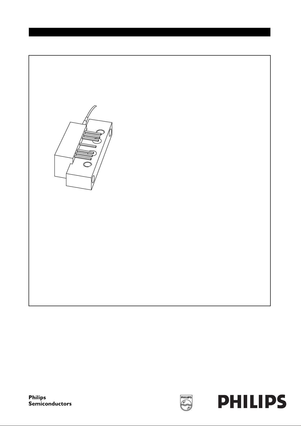
andbook, halfpage
M3D112
BGY887BO/FC1
Optical receiver module
Product specification
Supersedes data of 1998 Feb 02
File under Discrete Semiconductors, SC16
1998 Mar 13

Philips Semiconductors Product specification
Optical receiver module BGY887BO/FC1
FEATURES
• Excellent linearity
• Extremely low noise
• Excellent flatness
• Standard CATV outline
• Rugged construction
• Gold metallization ensures excellent reliability
• FC/APC connector (JDS version).
APPLICATIONS
• CATV systems operating over a frequency range of
40 to 860 MHz.
DESCRIPTION
Hybrid high dynamic range optical receiver module in a
SOT115R package operating at a voltage supply of 24 V
(DC). The module contains a monomode optical input
suitable for wavelengths from 1290 to 1600 nm, a terminal
to monitor the pin diode current and an electrical output
with an impedance of 75 Ω.
The optical fibre is terminated by an FC/APC connector
(JDS version) and partly reinforced by a 3 mm diameter
Kevlar buffer.
PINNING - SOT115R
PIN DESCRIPTION
1 monitor current
2 common
3 common
5+V
7 common
8 common
9 output
handbook, halfpage
2
Side view
B
789
351
MBK045
Fig.1 Simplified outline
QUICK REFERENCE DATA
SYMBOL PARAMETER CONDITIONS MIN. MAX. UNIT
f frequency range 40 860 MHz
S
22
output return losses f = 40 to 860 MHz 11 − dB
optical input return losses 40 − dB
d
2
second order distortion f = 324.25 MHz −−70 dBc
F equivalent noise input f = 40 MHz − 7 pA/√Hz
I
tot
total current consumption (DC) VB= 24 V 175 205 mA
CAUTION
This product is supplied in anti-static packing to prevent damage caused by electrostatic discharge during transport
and handling. For further information, refer to Philips specs.: SNW-EQ-608, SNW-FQ-302A, and SNW-FQ-302B.
HANDLING
Fibreglass optical coupling: maximum tensile strength = 5 N; minimum bending radius = 35 mm.
1998 Mar 13 2
Philips Semiconductors Product specification
Optical receiver module BGY887BO/FC1
LIMITING VALUES
In accordance with the Absolute Maximum Rating System (IEC 134).
SYMBOL PARAMETER CONDITIONS MIN. MAX. UNIT
f frequency range 40 860 MHz
T
stg
T
mb
P
in
ESD ESD sensitivity human body model;
CHARACTERISTICS
Bandwidth 40 to 860 MHz; V
SYMBOL PARAMETER CONDITIONS MIN. MAX. UNIT
S responsivity λ = 1300 nm 750 − V/W
FL flatness of frequency response −±0.5 dB
S
22
OBR
IL
C
d
2
d
3
F equivalent noise input f
s
λ
λ optical wavelength 1290 1600 nm
L length of optical fibre buffered fibre; SM type; 9/125 µm;
I
tot
storage temperature range −40 +85 °C
operating mounting-base temperature −20 +85 °C
optical input power continuous − 5mW
500 − V
R = 1.5 kΩ; C = 100 pF
= 24 V; Tmb=30°C; ZS=ZL=75Ω.
B
output return losses f = 40 to 860 MHz 11 − dB
optical input return losses 40 − dB
connector optical return losses 70 − dB
C
connector optical insertion losses − 0.5 dB
second order distortion note 1 −−70 dB
third order distortion note 2 −−80 dB
=40MHz − 7 pA/√Hz
1
spectral sensitivity λ = 1310 ±20 nm 0.85 − A/W
λ = 1550 ±20 nm 0.9 − A/W
817 917 mm
Kevlar buffer: 3 mm
total current consumption note 3 175 205 mA
Notes
1. Two laser test; each laser with 40% modulation index:
fp= 135 MHz; Pp= 0.5 mW;
fq= 189.25 MHz; Pq= 0.5 mW;
measured at fp+fq= 324.25 MHz.
2. Three laser test; each laser with 40% modulation
index:
fp= 326.25 MHz; Pp= 0.33 mW;
fq= 333.25 MHz; Pq= 0.33 mW;
fr= 335.25 MHz; Pr= 0.33 mW;
measured at fp+fq−fr= 324.25 MHz.
3. The module normally operates at VB= 24 V, but is
able to withstand supply transients up to 30 V.
1998 Mar 13 3
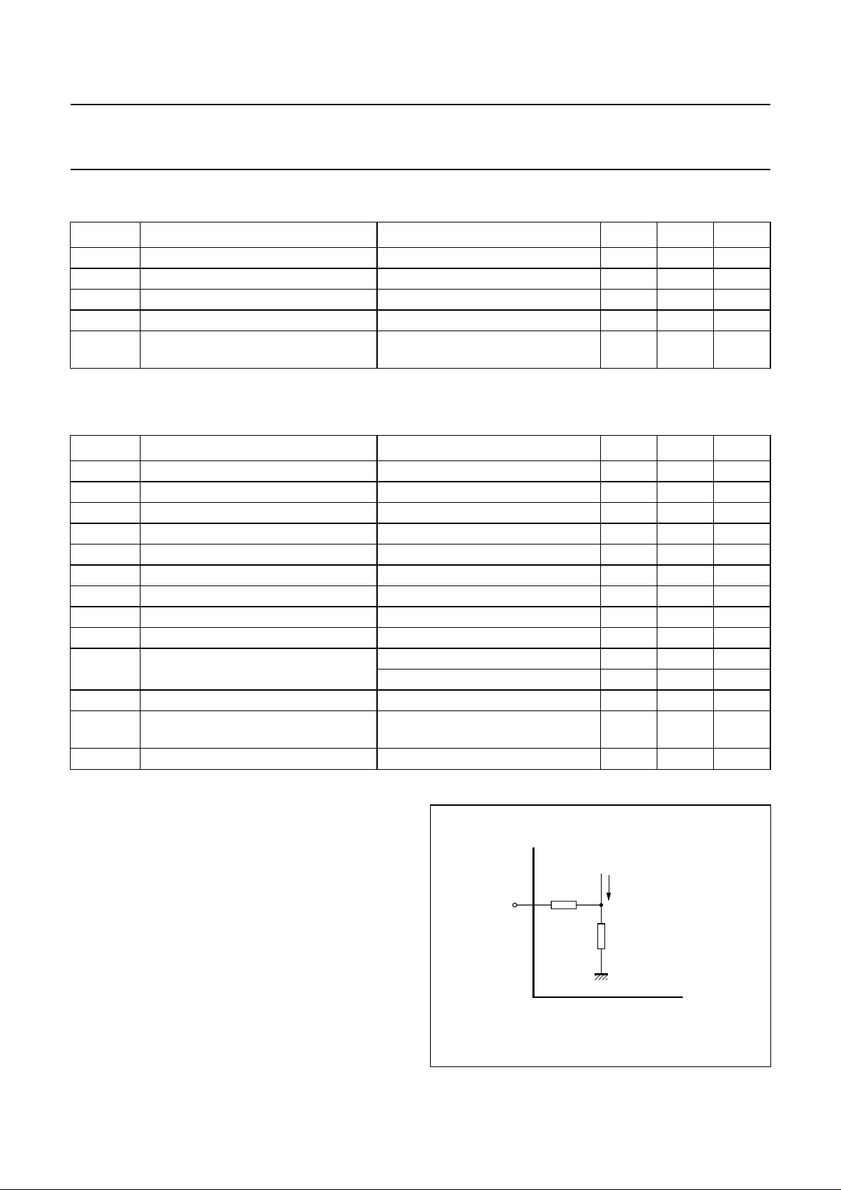
handbook, halfpage
photo
Pin 1
10 kΩ
current
1 kΩ
Fig.2 Monitor current pin.
MLB151
 Loading...