

Philips BGY685AD User Manual
DISCRETE SEMICONDUCTORS
DATA SH EET
ook, halfpage
M3D252
BGY685AD
600 MHz, 18.5 dB gain push-pull
amplifier
Product specification
Supersedes data of 1997 Apr 18
2001 Oct 22
Philips Semiconductors Product specification
600 MHz, 18.5 dB gain push-pull amplifier BGY685AD
FEATURES
• Excellent linearity
• Extremely low noise
• Silicon nitride passivation
• Rugged construction
• Gold metallization ensures
excellent reliability.
APPLICATIONS
• CATV systems operating over a
40 to 600 MHz frequency range.
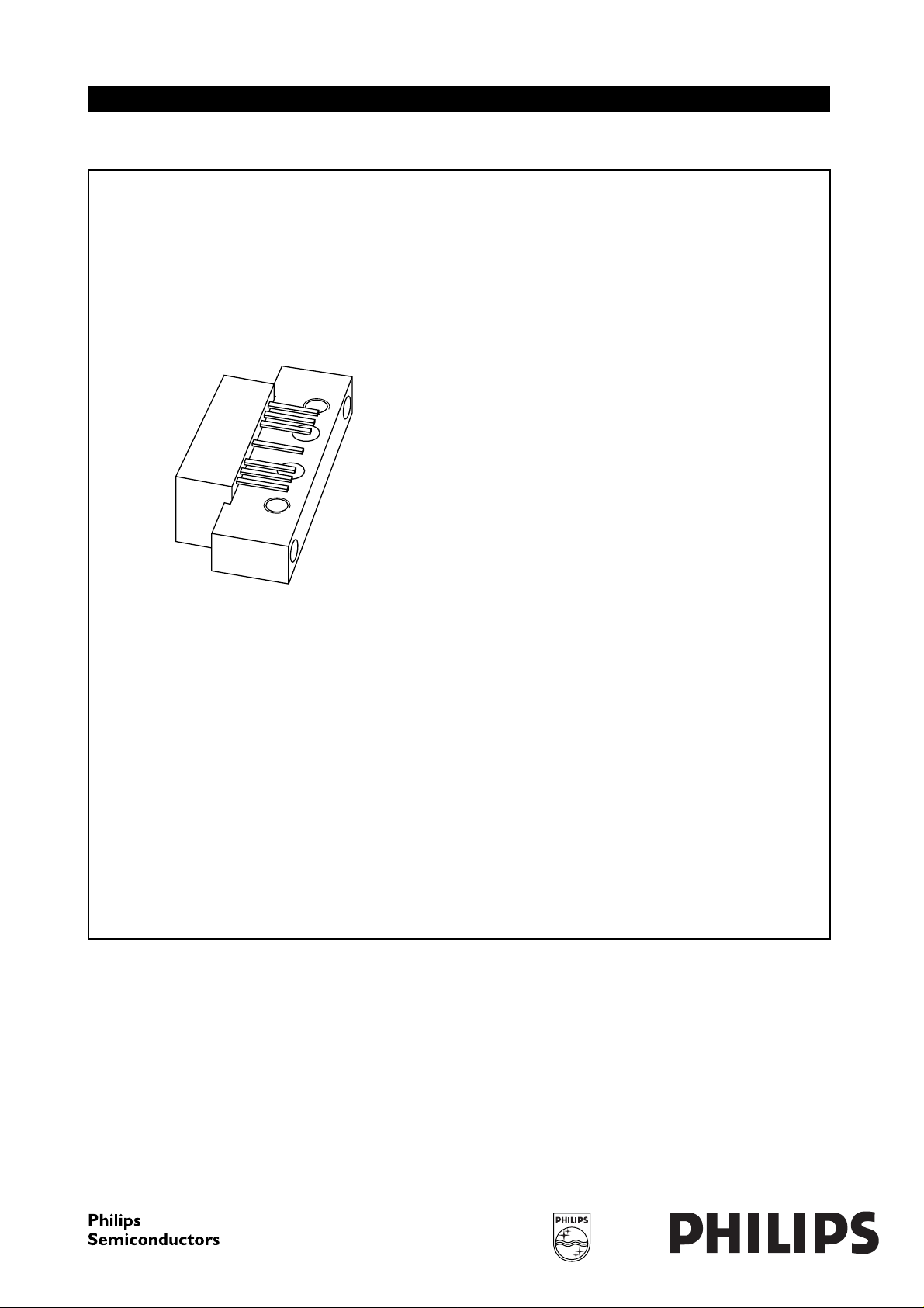
DESCRIPTION
Hybrid high dynamic range cascode
amplifier module with Darlington
pre-stage dies operating at a voltage
supply of +24 V in a SOT115J
package.
QUICK REFERENCE DATA
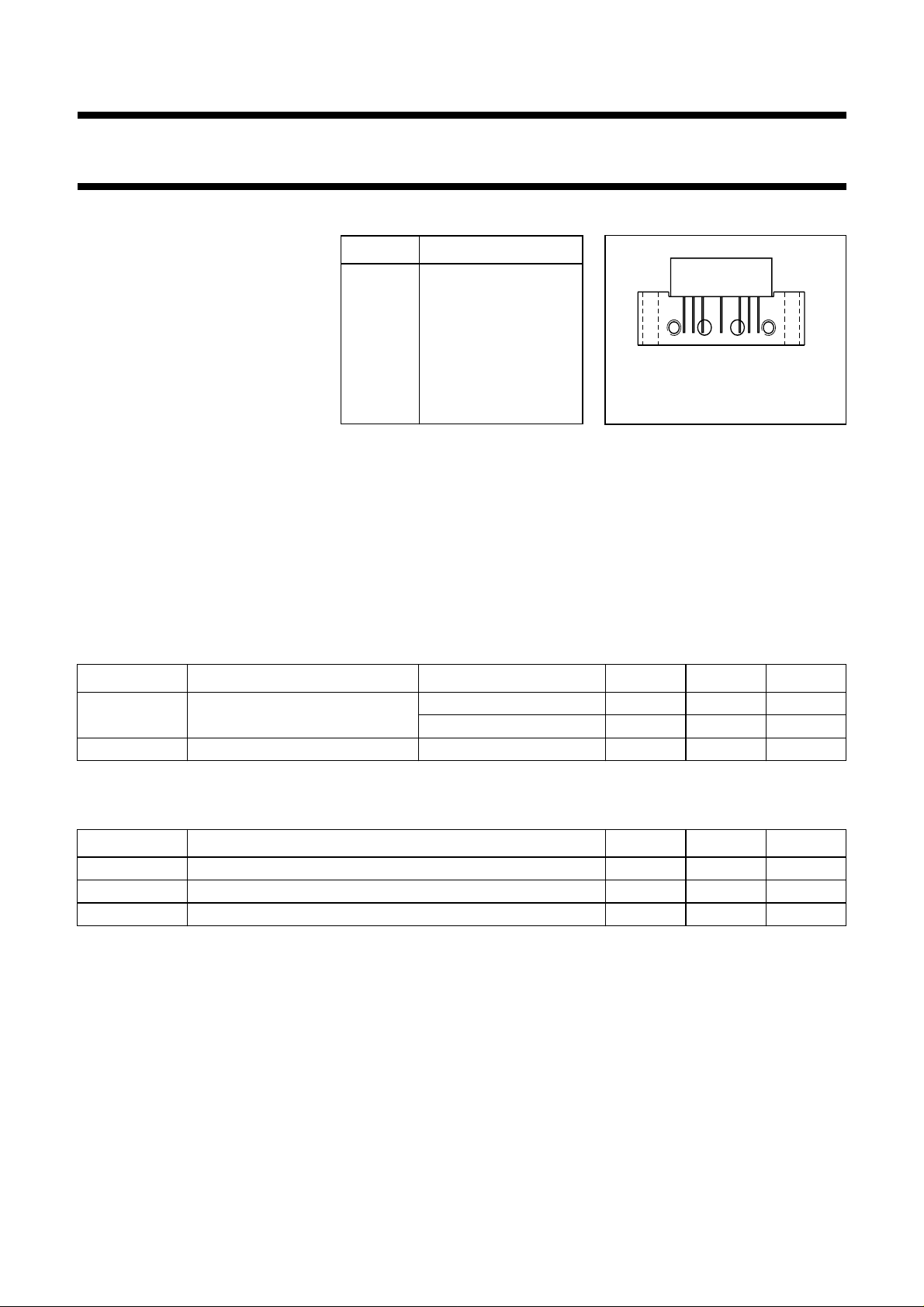
PINNING - SOT115J
PIN DESCRIPTION
1 input
2 common
3 common
5+V
B
7 common
8 common
9 output
page
2
351
Side view
Fig.1 Simplified outline.
789
MSA319
SYMBOL PARAMETER CONDITIONS MIN. MAX. UNIT
G
p
power gain f = 50 MHz 18 19 dB
f = 600 MHz 18.75 − dB
I
tot
total current consumption (DC) VB=24V − 250 mA
LIMITING VALUES
In accordance with the Absolute Maximum Rating System (IEC 60134).
SYMBOL PARAMETER MIN. MAX. UNIT
V
i
T
stg
T
mb
RF input voltage − 60 dBmV
storage temperature −40 +100 °C
operating mounting base temperature −20 +100 °C
2001 Oct 22 2
Philips Semiconductors Product specification
600 MHz, 18.5 dB gain push-pull amplifier BGY685AD
CHARACTERISTICS
Table 1 Bandwidth 40 to 600 MHz; VB= 24 V; T
=30°C; ZS=ZL=75Ω
case
SYMBOL PARAMETER CONDITIONS MIN. MAX. UNIT
G
p
power gain f = 50 MHz 18 19 dB
f = 600 MHz 18.75 − dB
SL slope cable equivalent f = 40 to 600 MHz 0.2 2.2 dB
FL flatness of frequency response f = 40 to 600 MHz −±0.3 dB
S
11
input return losses f = 40 to 80 MHz 20 − dB
f = 80 to 160 MHz 19 − dB
f = 160 to 600 MHz 18 − dB
S
22
output return losses f = 40 to 80 MHz 20 − dB
f = 80 to 160 MHz 19 − dB
f = 160 to 600 MHz 18 − dB
S
21
CTB composite triple beat 85 channels flat;
phase response f = 50 MHz −45 +45 deg
−−62 dB
V
= 44 dBmV;
o
measured at 595.25 MHz
X
mod
cross modulation 85 channels flat;
−−58 dB
Vo= 44 dBmV;
measured at 55.25 MHz
CSO composite second order distortion 85 channels flat;
V
= 44 dBmV;
o
−−60 dB
measured at 596.5 MHz
d
2
V
o
second order distortion note 1 −−70 dB
output voltage dim= −60 dB; note 2 62 − dBmV
F noise figure f = 50 MHz − 6dB
f = 600 MHz − 8dB
I
tot
total current consumption (DC) note 3 − 250 mA
Notes
p=Vq
= 44 dBmV;
1. V
fp= 55.25 MHz; fq= 541.25 MHz;
measured at fp+fq= 596.5 MHz.
2. Measured according to DIN45004B:
fp= 590.25 MHz; Vp=Vo;
fq= 597.25 MHz; Vq=Vo−6 dB;
fr= 599.25 MHz; Vr=Vo−6 dB;
measured at fp+fq−fr= 588.25 MHz.
3. The module normally operates at VB= 24 V, but is able to withstand supply transients up to 30 V.
2001 Oct 22 3
 Loading...