

Philips BGY212A Datasheet
DISCRETE SEMICONDUCTORS
DATA SHEET
ook, halfpage
M3D373
BGY212A
UHF amplifier module
Preliminary specification 1999 Aug 23
Philips Semiconductors Preliminary specification
UHF amplifier module BGY212A
FEATURES
• 3.5 V nominal supply voltage
• 2 W output power
• Easy output power control by DC voltage.
APPLICATIONS
• Digital cellular radio systems with Time Division Multiple
Access (TDMA) operation (GSM systems) in the
1710 to 1785 MHz frequency range.
DESCRIPTION
The BGY212A is a three-stage UHF amplifier module in a
SOT482C leadless package with a plastic cover. The
module consists of one NPN silicon planar transistor die
and one bipolar monolithic integrated circuit mounted
together with matching and bias circuit components on a
metallized ceramic substrate.
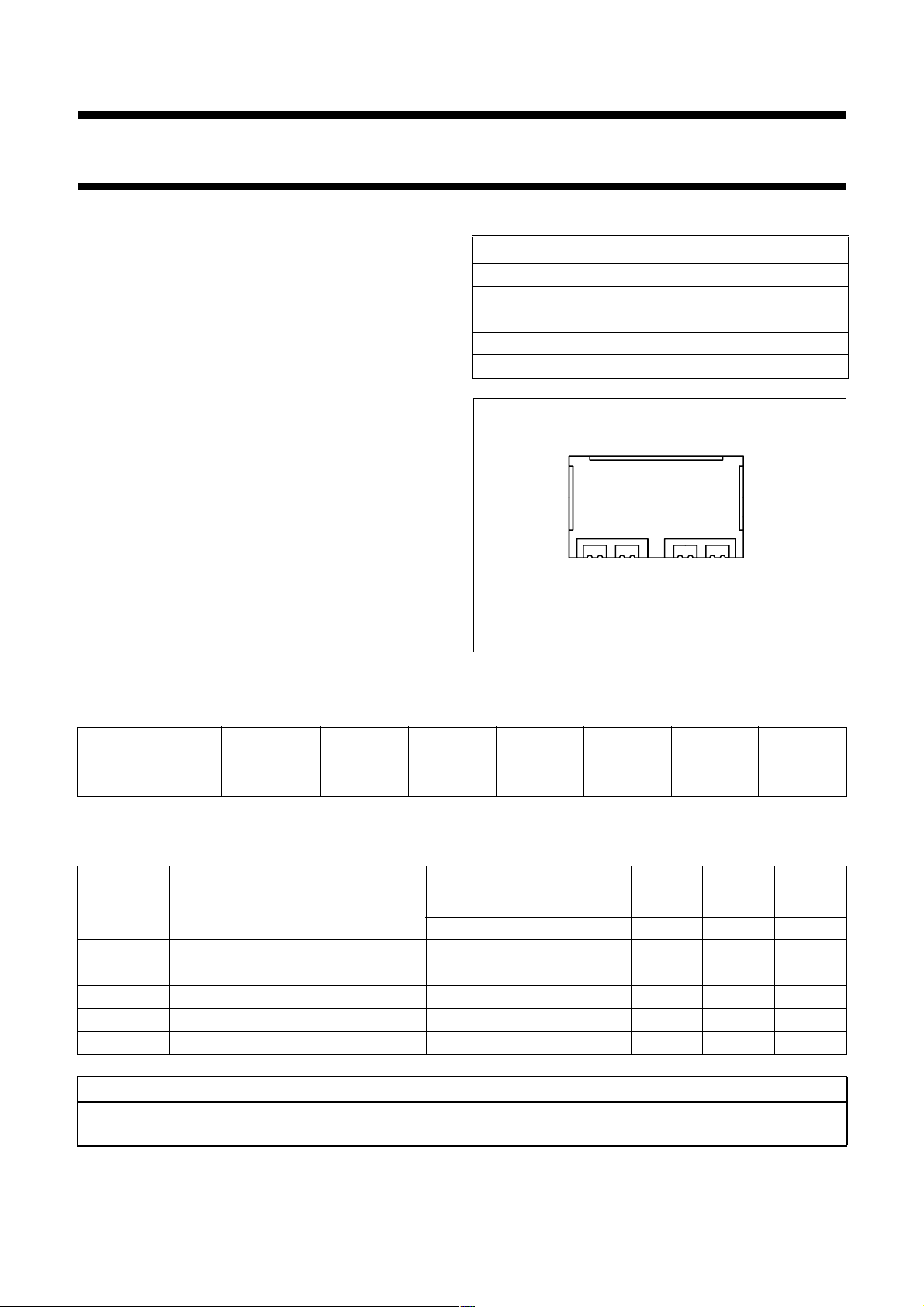
PINNING - SOT482C
PIN DESCRIPTION
1 RF input
2V
3V
4 RF output
5 ground
ok, halfpage
43 251
Bottom view
Fig.1 Simplified outline
C
S
MBK201
QUICK REFERENCE DATA
RF performance at T
MODE OF
OPERATION
=25°C.
mb
f
(MHz)
V
(V)
S
V
C
(V)
P
L
(dBm)
G
(dB)
p
η
(%)
, Z
Z
S
(Ω)
Pulsed; δ = 1 : 8 1710 to 1785 3.5 ≤2.2 typ.33 typ.33 typ.40 50
LIMITING VALUES
In accordance with the Absolute Maximum Rating System (IEC 134).
SYMBOL PARAMETER CONDITIONS MIN. MAX. UNIT
V
S
V
C
P
D
P
L
T
stg
T
mb
DC supply voltage VC< 0.2 V; PD=0mW − 7V
V
≥ 0.2 V − 4.1 V
C
DC control voltage − 2.7 V
input drive power − 10 dBm
load power − 34.1 dBm
storage temperature −40 +100 °C
operating mounting base temperature −30 +100 °C
CAUTION
This product is supplied in anti-static packing to prevent damage caused by electrostatic discharge during transport
and handling. For further information, refer to Philips specs.: SNW-EQ-608, SNW-FQ-302A and SNW-FQ-302B.
L
1999 Aug 23 2
Philips Semiconductors Preliminary specification
UHF amplifier module BGY212A
CHARACTERISTICS
Z
otherwise specified.
I
I
P
G
η efficiency P
H
H
VSWR
P
t
t
=50Ω; PD=0dBm; VS= 3.5 V; VC≤ 2.2 V; f = 1710 to 1785 MHz; Tmb=25°C; δ =1:8; tp= 575 µs unles
S=ZL
SYMBOL PARAMETER CONDITIONS MIN. TYP. MAX. UNIT
Q
CM
L
p
2
3
leakage current VC=0.2V −−10 µA
V
= 0.2 V; VS=7V − 520mA
C
peak control current adjust VC for PL=32dBm −−3mA
load power VC= 2.2 V; VS=3.5V − 33.2 − dBm
V
= 2.2 V; VS= 3.2 V 32 32.3 − dBm
C
V
= 2.2 V; VS=3.2V; Tmb=85°C 31 31.8 − dBm
C
power gain PL=32dBm − 32 − dB
=32dBm − 40 − %
L
second harmonic PL=32dBm −−−35 dBc
third harmonic PL=32dBm −−−40 dBc
input VSWR PL= 2 to 32 dBm − 3:1
in
stability V
= 3.2 to 4.1 V; PD= −3to3dBm;
S
=0to2.2V; PL≤ 33 dBm;
V
C
−−−60 dBc
VSWR ≤ 8 : 1 through all phases
isolation V
= 0.2 V; PD=3dBm −−36 −33 dBm
C
control bandwidth tbd −−MHz
n
noise power PL= 2 to 32 dBm;
−−73 −71 dBm
bandwidth = 100 kHz; 20 MHz above
transmission band
AM/AM conversion P
AM/PM conversion P
control slope P
T
conversion PL= 32 dBm; f = 1785 MHz
X/RX
r
f
carrier rise time PL= 2 to 32 dBm; time to settle
carrier fall time PL= 2 to 32 dBm; time to fall below
with 3% AM; f = 100 kHz;
D
P
= 2 to 32 dBm
L
= −0.5to0.5dBm;
D
= 2 to 32 dBm
P
L
= −8to+2dBm − tbd − dB / V
L
P
= 2 to 32 dBm − tbd − dB / V
L
P
(1805 MHz) / PD(1765 MHz)
L
within −0.5 dB of final P
L
− 58%
−−tbd deg/dB
− 28 30 dB
− 1.5 2 µs
− 1.5 2 µs
− 33 dBm
ruggedness V
= 4.1 V; adjust VC for
S
P
= 33 dBm; VSWR ≤ 8 : 1 through
L
no degradation
all phases
1999 Aug 23 3
Philips Semiconductors Preliminary specification
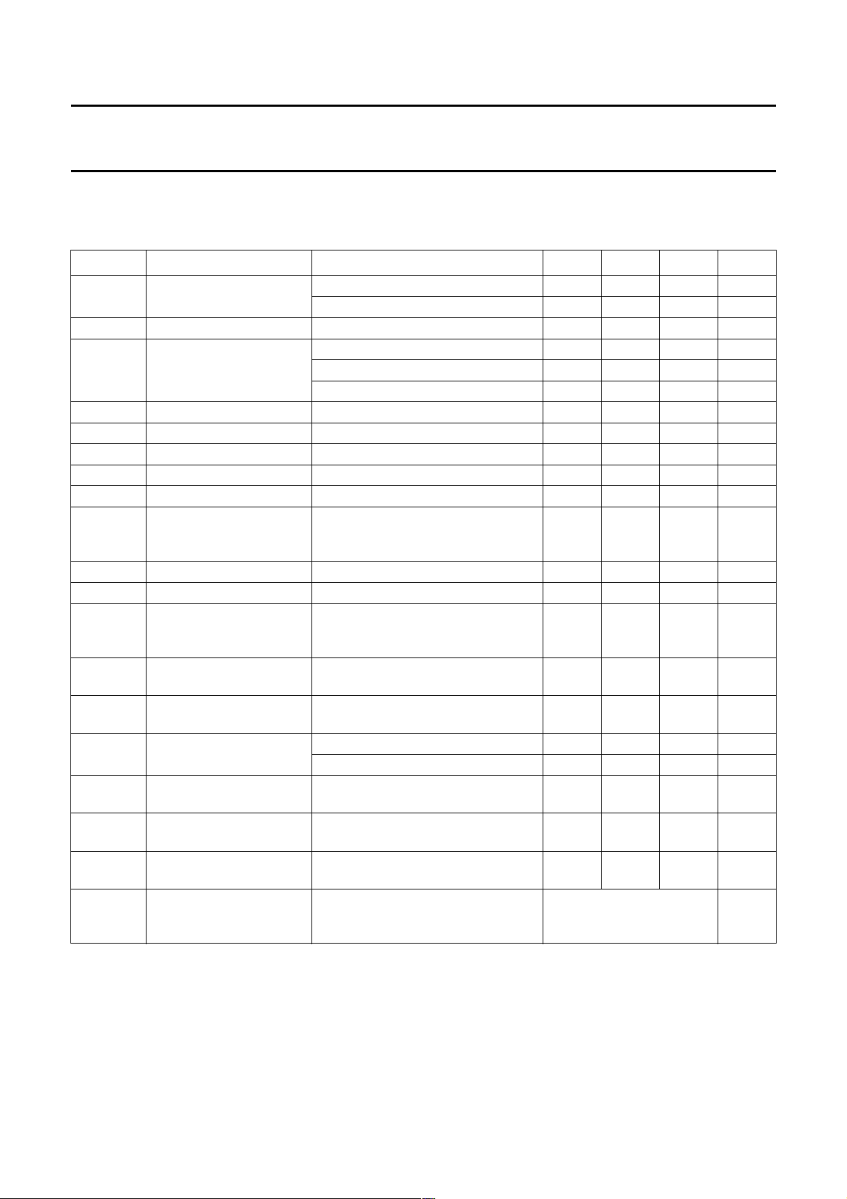
Fig.2 Load power as a function of control voltage;
typical values.
ZS=ZL=50Ω; VS= 3.5 V; PD=0dBm;
T
mb
=25°C; δ =1:8; tp=575µs.
Fig.4 Efficiency as a function of load power;
typical values.
ZS=ZL=50Ω; VS= 3.5 V; PD=0dBm;
T
mb
=25°C; δ =1:8; tp=575µs.
UHF amplifier module BGY212A
3
P
L
(W)
2
1710MHz
1785MHz
1
0
11.522.5
V
(V)
C
4
P
L
(W)
3
1710MHz
1785MHz
2
1
0
2345
(V)
V
S
ZS=ZL=50Ω; VC=2.2V; PD=0dBm;
=25°C; δ =1:8; tp= 575 µs.
T
mb
Fig.3 Load power as a function of supply voltage;
typical values.
50
η
(%)
40
30
20
10
0
00.511.522.5
1999 Aug 23 4
1785MHz
1710MHz
(W)
P
L
3
P
L
(W)
2
1
0
1700 1750 1800
f (MHz)
ZS=ZL=50Ω; VS= 3.5 V; PD=0dBm; VC=2.2V;
=25°C; δ =1:8; tp=575µs.
T
mb
Fig.5 Load power as a function of frequency;
typical values.
 Loading...