

DISCRETE SEMICONDUCTORS
DATA SH EET
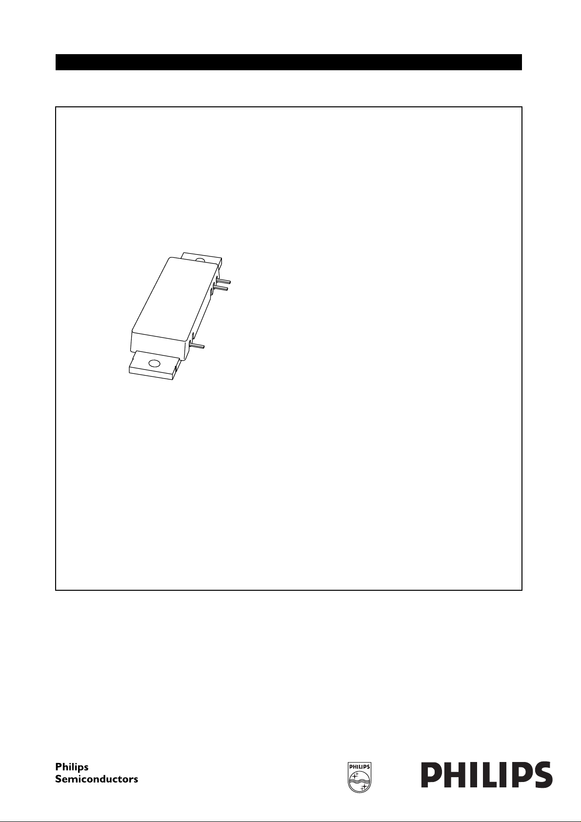
M3D737
BGF802-20
CDMA800 power module
Product specification
Supersedes data of 2002 Nov 12
2003 Feb 24
Philips Semiconductors Product specification
CDMA800 power module BGF802-20
FEATURES
• Typical CDMAIS95 performance at a supply voltage of
28 V:
– Output power = 3 W
– Gain = 30 dB
– Efficiency = 18%
– ACPR < -53 dBc at 750 kHz and BW = 30 kHz
– ACPR < -69 dBc at 1.98 MHz and BW = 30 kHz.
• Low distortion to CDMA signals
• Excellent 2-tone performance
• Low die temperatures using copper flange
• Integrated temperature compensated bias
• 50 Ω input/output system
• Flat gain over frequency range.
APPLICATIONS
• Base station RF power amplifiers in the 869 to 894 MHz
frequency range
• CDMA IS95, CDMA2000, multi carrier applications
• Macrocell (driver stage) and Microcell (final stage).
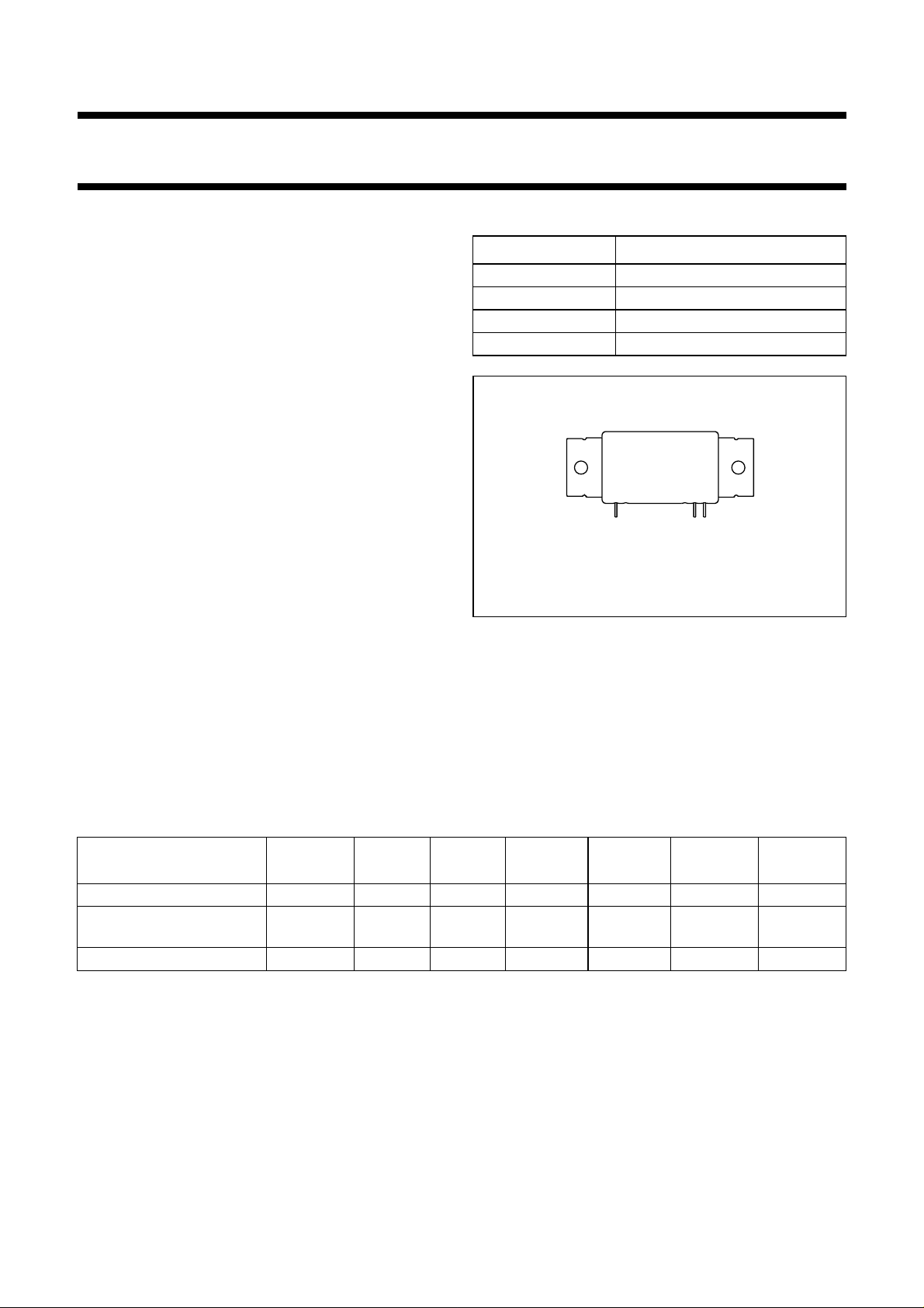
PINNING - SOT365C
PIN DESCRIPTION
1 RF input
2V
3 RF output
Flange ground
Top view
Fig.1 Simplified outline.
S
1
23
MBL257
DESCRIPTION
25 W LDMOS power amplifier module for base station
amplifier applications in the 869 to 894 MHz range.
QUICK REFERENCE DATA
Typical RF performance at Tmb=25°C.
MODE OF OPERATION
f
(MHz)
V
(V)
DS
P
(W)
L
G
(dB)
p
η
(%)
ACPR
(dBc)
EVM
(%)
CW 869 to 894 28 25 29 48 −−
IS95 CDMA
(1)
869 to 894 28 3 30 18 −53
GSM EDGE 869 to 894 26 2.5 30 16 −65
−69
(2)
(3)
(4)
−
0.4
Notes
1. IS95 CDMA (Pilot, paging, sync and traffic codes 8−13).
2. ACPR 750 kHz at 30 kHz resolution bandwidth.
3. ACPR 1.98 MHz at 30 kHz resolution bandwidth.
4. ACPR 400 kHz at 30 kHz resolution bandwidth.
2003 Feb 24 2
Philips Semiconductors Product specification
CDMA800 power module BGF802-20
LIMITING VALUES
In accordance with the Absolute Maximum Rating System (IEC 60134).
SYMBOL PARAMETER MIN. MAX. UNIT
V
S
P
D
P
L
T
stg
T
mb
CHARACTERISTICS
Tmb=25°C; VS= 28 V; PL= 3.0 W; f = 869 to 894 MHz; ZS=ZL=50Ω; unless otherwise specified.
SYMBOL PARAMETER CONDITIONS MIN. TYP. MAX. UNIT
I
DQ
P
1dB
G
p
∆G
p freq
∆G
p pwr
∆ϕ
freq
G
OB
VSWR
in
H
2
H
3
IS95 CDMA (PL= 3 W average)
DC supply voltage − 30 V
input drive power − 100 mW
load power − 30 W
storage temperature −30 +100 °C
operating mounting base temperature −20 +90 °C
quiescent current (pin 2) PD= 0 mW 245 280 320 mA
load power at 1 dB gain compression 18 25 − W
power gain 28 30 32 dB
gain flatness over
− 0.2 1.0 dB
frequency range
gain flatness over power
PL= 30 mW up to 3 W −0.8 −0.2 0.2 dB
band
phase linearity over
− 0.2 − deg
frequency range
delay flatness − 200 − ps
out of band gain small signal, PD= 0 dBm;
f < 869 MHz, f > 894 MHz
−−G
Pimax
+1
note 1
dB
input VSWR − 1.6:1 2.0:1
second harmonic −−37 −34 dBc
third harmonic −−61 −58 dBc
stability VSWR ≤ 3 : 1 through all
phases; V
=25to28V
S2
ruggedness VSWR = 10 : 1 through all
phases; P
=5W
L
all spurious outputs more than 60 dB
below desired signal
no degradation in output power
η efficiency 15 18 − %
ACPR
ACPR
750 kHz
1.98 MHz
spectral regrowth;
measured in 30 kHz RBW
−−53 −49 dBc
−−69 −66 dBc
Note
1. G
is small signal in-band gain.
Pi
2003 Feb 24 3
Philips Semiconductors Product specification
CDMA800 power module BGF802-20
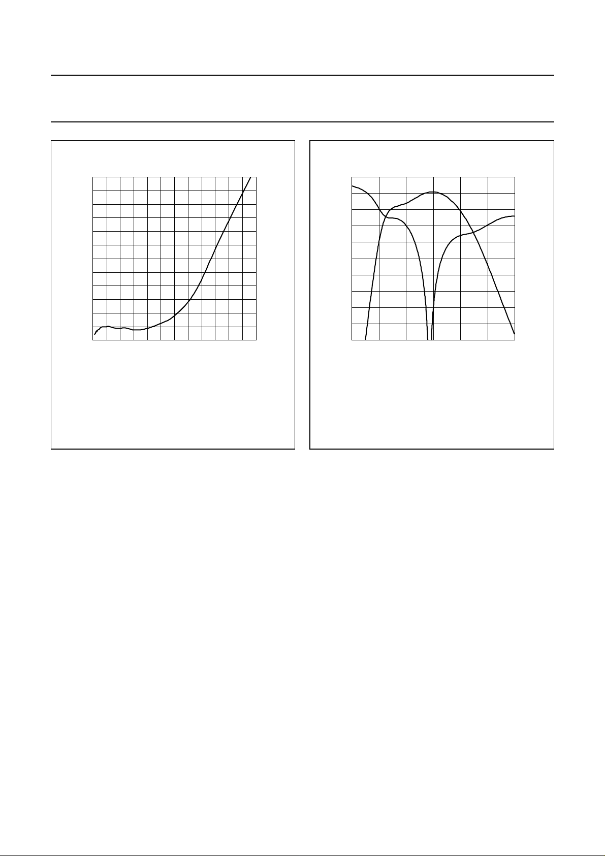
6
P
L (AV)
MBL762
(W)
30.4
handbook, halfpage
G
p
(dB)
30
29.6
29.2
28.8
024 8
f = 882 MHz.
G
p
η
Fig.2 IS95 power gain and efficiency as functions
of load power; typical values.
40
30
20
10
0
(%)
−40
handbook, halfpage
ACPR
η
750 kHz
(dBc)
−45
−50
−55
−60
−65
f = 882 MHz.
024 8
MBL763
6
P
L (AV)
(W)
Fig.3 ACPR at 750 kHz as a function of output
power; typical values.
6
P
L (AV)
MBL764
(W)
−60
handbook, halfpage
ACPR
1.98 MHz
(dBc)
−64
−68
−72
−76
024 8
f = 882 MHz.
Fig.4 ACPR at 1.98 MHz as a function of output
power; typical values.
30.4
handbook, halfpage
G
p
(dB)
30
29.6
29.2
28.8
28.4
28
010203051525
f = 882 MHz.
G
p
MBL765
η
PL (W)
Fig.5 CW power gain and efficiency as functions
of load power; typical values.
60
50
40
30
20
10
0
(%)
η
2003 Feb 24 4

Philips Semiconductors Product specification
CDMA800 power module BGF802-20
30.4
handbook, halfpage
G
p
(dB)
30
29.6
29.2
28.8
048 16
f1= 882 MHz; f2= 883 MHz.
G
p
12
η
P
L (AV)
Fig.6 Two tone power gain and efficiency as
functions of load power; typical values.
MBL766
(W)
48
36
24
12
0
(%)
12
P
L (AV)
MBL767
(W)
−20
handbook, halfpage
d
η
im
(dBc)
−30
−40
−50
−60
−70
048 16
f1= 882 MHz; f2= 883 MHz.
d3d
5
d
7
Fig.7 Two tone intermodulation distortion as
function of load power; typical values.
P
L (AV)
MBL768
(W)
−58
handbook, halfpage
ACPR
400 kHz
(dBc)
−60
−62
−64
−66
−68
0
f = 882 MHz.
412
82610
Fig.8 GSMEDGEACPRat400 kHz as a function
of load power; typical values.
P
L (AV)
MBL769
handbook, halfpage
4
EVM
rms
(%)
3
2
1
0
04 12
f = 882 MHz.
82610
Fig.9 GSM EDGE rms EVM as a function of load
power; typical values.
(W)
2003 Feb 24 5
Philips Semiconductors Product specification
CDMA800 power module BGF802-20
P
L (AV)
MBL770
12
handbook, halfpage
EVM
M
(%)
10
8
6
4
2
0
04 12
f = 882 MHz.
82610
Fig.10 GSM EDGE peak EVM asafunctionof load
power; typical values.
(W)
31
handbook, halfpage
s
21
(dB)
s
29
27
25
23
21
750 850 950 1050
11
s
21
s
f (MHz)
Fig.11 s-parameters as a function of frequency.
MBL771
11
0
−6
−12
−18
−24
−30
s
11
(dB)
2003 Feb 24 6

Philips Semiconductors Product specification
CDMA800 power module BGF802-20
MOUNTING RECOMMENDATIONS
General
LDMOST base station modules are manufacturedwith the
dies directly mounted onto a copper flange. The matching
and bias circuit components are mounted on a
printed-circuit board (PCB), which is also soldered onto
thecopperflange.ThediesandthePCBareencapsulated
in a plastic cap, and pins extending from the module
provideameansofelectricalconnection.Thisconstruction
allows the module to withstand a limited amount of flexing,
although bending of the module is to be avoided as much
as possible. Mechanical stress can occur if the bottom
surface of the module and the surface of the amplifier
casing (external heatsink) are not mutually flat. This,
therefore, should be a consideration when mounting the
module in the amplifier. Another cause of mechanical
stress can arise from thermal mismatch after soldering of
the pins. Precautions should be taken during soldering,
and efforts made to ensure a good thermal contact
between the flange and the external heatsink.
External heatsink (amplifier casing)
The module should always be mounted on a heatsink with
a low thermal resistance to keep the module temperature
as low as possible. The mounting area of the heatsink
should be flat and free from burrs and loose particles. We
recommend a flatness for the mounting area of between
50 µm concave and 50 µm convex. The 50 µm concave
value is to ensure optimal thermal behaviour, while the
50 µm convex value is intended to limit mechanical stress
due to bending.
CAUTION
During the following procedures ESD precautions should
be taken to protect the device from electrostatic damage.
PROCEDURE
1. Applyathin, evenly spread layer of thermal compound
to the module flange bottom surface. Excessive use of
thermal compound may result in increased thermal
resistance and possible bending of the of the flange.
Too little thermal compound will result in an increase
in thermal resistance.
2. Take care that there is some space between the cap
and the PCB. Bring the module into contact with the
external heatsink casing, ensuring that there is
sufficient space for excessive thermal compound to
escape.
3. Carefully align the module with the heatsink casing
mounting holes, and secure with two 3 mm bolts and
two flat washers. Initially tighten the bolts to “finger
tight” (approximately 0.05 Nm). Using a torque
wrench, tighten each bolt in alternating steps to a final
torque of 0.4 Nm.
4. After the module is secured to the casing, the module
leads may be soldered to the PCB. The leads are for
electrical connection only, and should not be used to
support the module at any time in the assembly
process.
A soldering iron may be used up to a temperature of
250 °C for a maximum of 10 seconds. Avoid contact
between the soldering iron and the plastic cap.
In order to ensure optimal thermal behaviour, the use of
thermal compound is recommended when mounting the
module onto the amplifier external heatsink.
The following recommended thermal compounds have a
thermal conductivity of >0.5 W/mK:
• WPS II (silicone-free) from Austerlitz-Electronics
• Comp. Trans. from KF
• 340 from Dow Corning
• Trans-Heat from E. Friis-Mikkelsen.
The use of thermal pads instead of thermal compound is
not recommended as the pads may not maintain a uniform
flatness over a period of time.
Mounting
PREPARATION
Ensure that the surface finishes are free from burrs, dirt
and grease.
2003 Feb 24 7
Electrical connections
The main ground path of all modules is via the flange. It is
therefore important that the flange is well grounded and
that return paths are kept as short as possible. An
incorrectly grounded flange can result in a loss of output
power or in oscillation.
The RF input and output of the module are designed for
50 Ω connections.
Incoming inspection
When incoming inspection is performed, use a properly
designed test fixture to avoid excessive mechanical stress
and to ensure optimal RF performance. Philips can deliver
dedicated test fixtures on request.

Philips Semiconductors Product specification
CDMA800 power module BGF802-20
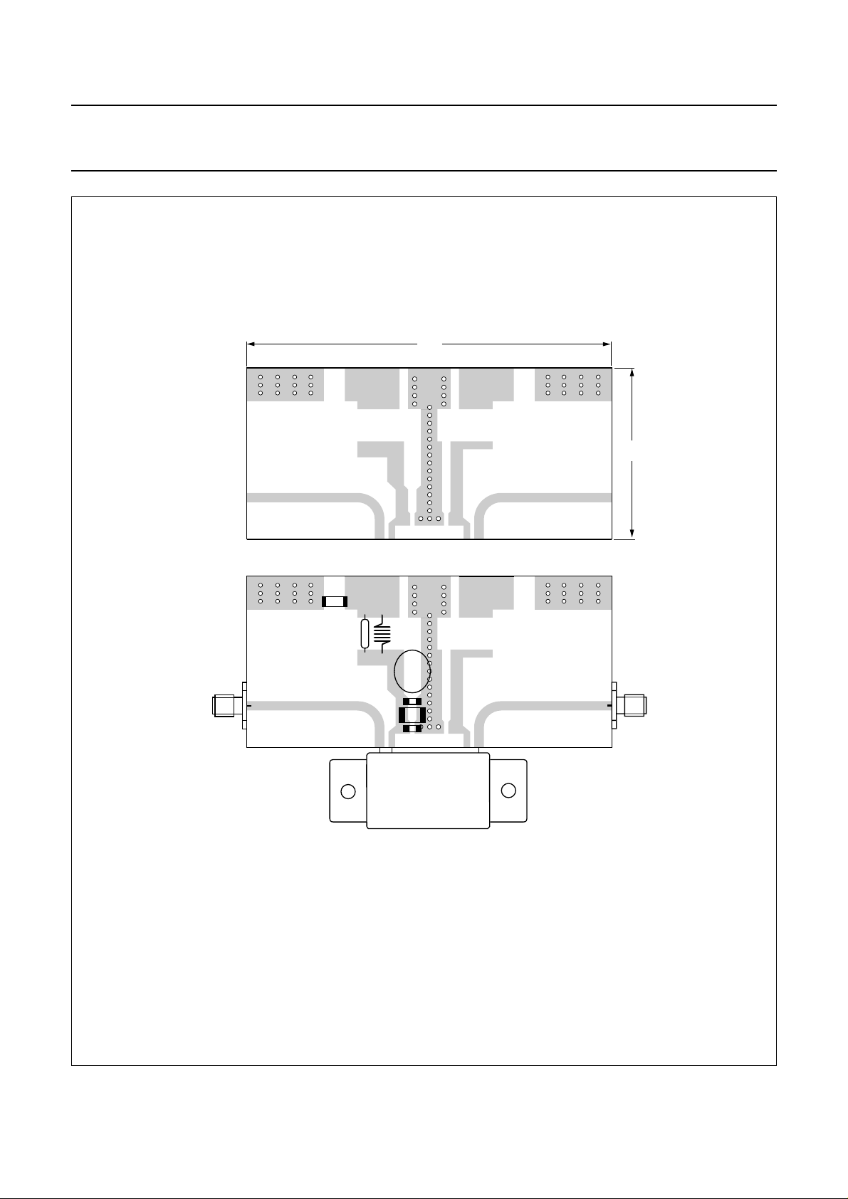
APPLICATION INFORMATION
handbook, halfpage
TEMPERATURE
COMPENSATED
GATE BIAS
C1
C2
C3
C4
+
Z
50 Ω
input
1
MBL781
R1 L1
C5
V
S
Z
2
50 Ω
output
Fig.12 Test circuit.
List of components (see Figs 12 and 13)
COMPONENT DESCRIPTION VALUE
CATALOGUE
NUMBER
C1, C3 multilayer X7R ceramic chip capacitor 100 nF; 50 V
C2, C5 tantalum SMD capacitor 10 µF; 35 V
C4 electrolytic capacitor 100 µF; 35 V
L1 grade 4S2 Ferroxcube bead 4330 030 36300
R1 metal film resistor 2322 195 13109
Z
, Z
1
2
stripline; note 1 50 Ω
Note
1. The striplines are on a double copper-clad printed-circuit board (RO5880) with εr= 2.2 and thickness = 0.79 mm.
2003 Feb 24 8
Philips Semiconductors Product specification
CDMA800 power module BGF802-20
handbook, full pagewidth
output
50 Ω
90
42
C5
C4
C2
C3
L1
input
50 Ω
C1
Z
1
R1
Z
2
DUT
Dimensions in mm.
Fig.13 Printed-circuit board and component layout.
2003 Feb 24 9
MBL780

Philips Semiconductors Product specification
CDMA800 power module BGF802-20
PACKAGE OUTLINE
Plastic rectangular single-ended flat package; flange mounted; 2 mounting holes; 3 in-line leads SOT365C
D
A
F
y
E
L
DIMENSIONS (mm are the original dimensions)
UNIT Qb Zc
A
0.56
mm
9.5
9.0
0.46
0.3
0.2
30.1
29.9
1
D
E
e
18.6
2.54
18.4
e
20.32
U
q
23
b
e
1
0 10 20 mm
1
3.3
3.1
3.7
3.3
e
scale
L
4.0
3.55
3.8
3.45
w M
Z
41.75
41.65
UFpq
48.4
48.0
U
p
U
15.4
15.2
3
A
v
A
vw
0.3 0.25
c
Q
y
12.8
0.1
12.6
3
U
2
U
1
U
U
2
1
7.75
1.1
7.55
0.0
OUTLINE
VERSION
SOT365C
IEC JEDEC JEITA
REFERENCES
2003 Feb 24 10
EUROPEAN
PROJECTION
ISSUE DATE
01-06-06
02-11-13

Philips Semiconductors Product specification
CDMA800 power module BGF802-20
DATA SHEET STATUS
LEVEL
DATA SHEET
STATUS
(1)
PRODUCT
STATUS
(2)(3)
DEFINITION
I Objective data Development This data sheet contains data from the objective specification for product
development. Philips Semiconductors reserves the right to change the
specification in any manner without notice.
II Preliminary data Qualification This data sheet contains data from the preliminary specification.
Supplementary data will be published at a later date. Philips
Semiconductors reserves the right to change the specification without
notice, in order to improve the design and supply the best possible
product.
III Product data Production This data sheet contains data from the product specification. Philips
Semiconductors reserves the right to make changes at any time in order
to improve the design, manufacturing and supply. Relevant changes will
be communicated via a Customer Product/Process Change Notification
(CPCN).
Notes
1. Please consult the most recently issued data sheet before initiating or completing a design.
2. The product status of the device(s) described in this data sheet may have changed since this data sheet was
published. The latest information is available on the Internet at URL http://www.semiconductors.philips.com.
3. For data sheets describing multiple type numbers, the highest-level product status determines the data sheet status.
DEFINITIONS
DISCLAIMERS
Short-form specification The data in a short-form
specification is extracted from a full data sheet with the
same type number and title. For detailed information see
the relevant data sheet or data handbook.
Limiting values definition Limiting values given are in
accordance with the Absolute Maximum Rating System
(IEC 60134). Stress above one or more of the limiting
values may cause permanent damage to the device.
These are stress ratings only and operation of the device
attheseoratanyotherconditions above those given in the
Characteristics sections of the specification is not implied.
Exposure to limiting values for extended periods may
affect device reliability.
Application information Applications that are
described herein for any of these products are for
illustrative purposes only. Philips Semiconductors make
norepresentationor warranty that such applications willbe
suitable for the specified use without further testing or
modification.
Life support applications These products are not
designed for use in life support appliances, devices, or
systems where malfunction of these products can
reasonably be expected to result in personal injury. Philips
Semiconductorscustomersusing or selling these products
for use in such applications do so at their own risk and
agree to fully indemnify Philips Semiconductors for any
damages resulting from such application.
Right to make changes Philips Semiconductors
reserves the right to make changes in the products including circuits, standard cells, and/or software described or contained herein in order to improve design
and/or performance. When the product is in full production
(status ‘Production’), relevant changes will be
communicated via a Customer Product/Process Change
Notification (CPCN). Philips Semiconductors assumes no
responsibility or liability for the use of any of these
products, conveys no licence or title under any patent,
copyright, or mask work right to these products, and
makes no representations or warranties that these
products are free from patent, copyright, or mask work
right infringement, unless otherwise specified.
2003 Feb 24 11

Philips Semiconductors – a w orldwide compan y
Contact information
For additional information please visit http://www.semiconductors.philips.com. Fax: +31 40 27 24825
For sales offices addresses send e-mail to: sales.addresses@www.semiconductors.philips.com.
© Koninklijke Philips Electronics N.V. 2003
All rights are reserved. Reproduction in whole or in part is prohibited without the prior written consent of the copyright owner.
The information presented in this document does not form part of any quotation or contract, is believed to be accurate and reliable and may be changed
without notice. No liability will be accepted by the publisher for any consequence of its use. Publication thereof does not convey nor imply any license
under patent- or other industrial or intellectual property rights.
Printed in The Netherlands 613524/04/pp12 Date of release: 2003 Feb 24 Document order number: 9397 750 10698
SCA75
 Loading...