

Page 1
DISCRETE SEMICONDUCTORS
DATA SH EET
ook, halfpage
M3D109
BGA6589
MMIC wideband medium power
amplifier
Product specification 2003 Sep 19
Page 2
Philips Semiconductors Product specification
MMIC wideband medium power amplifier BGA6589
FEATURES
• Broadband 50 Ω gain block
• 20 dBm output power
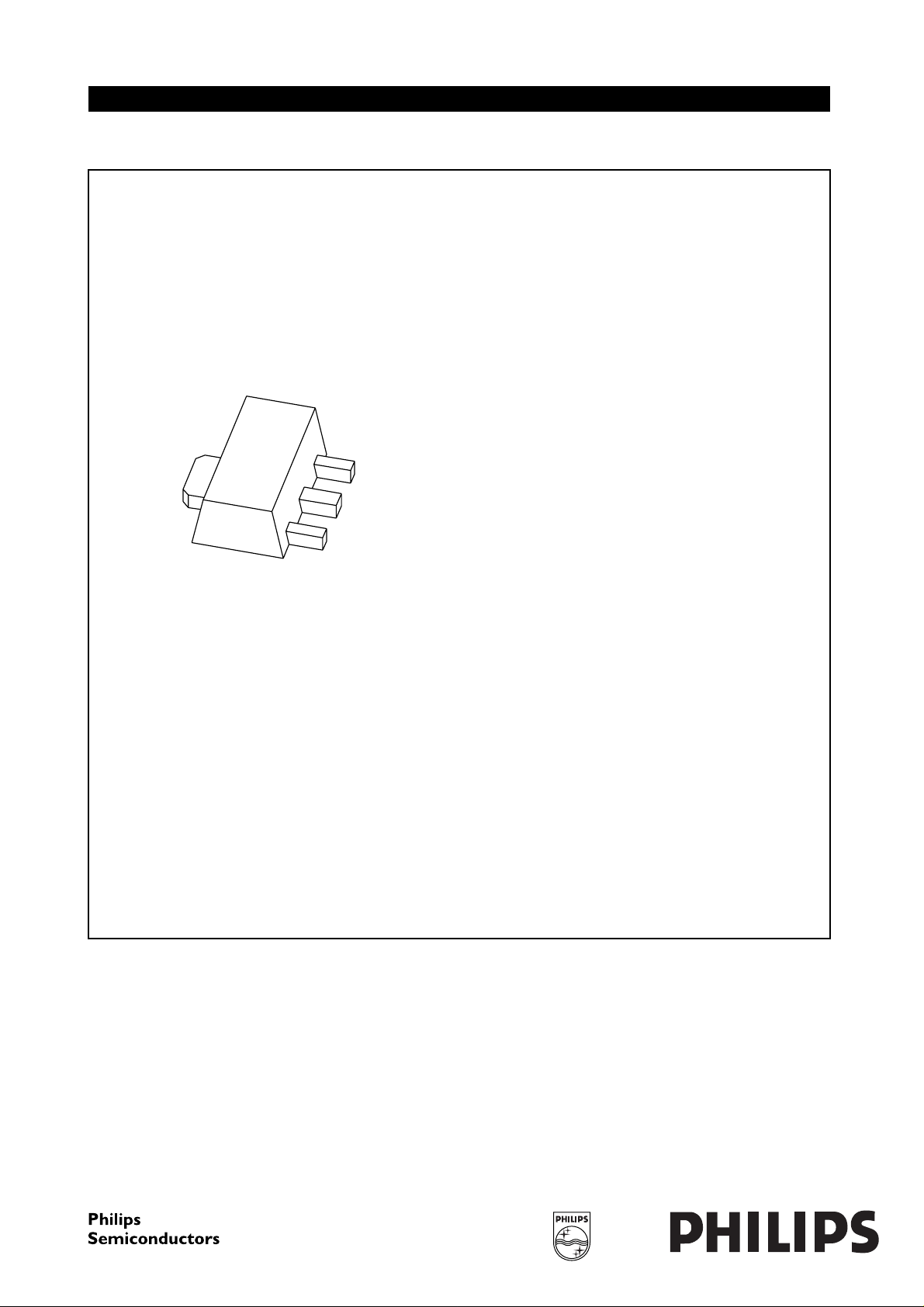
• SOT89 package
• Single supply voltage needed.
APPLICATIONS
• Broadband medium power gain blocks
• Small signal high linearity amplifiers
• Variable gainand high output power in combination with
the BGA2031
• Cellular, PCS and CDPD
• IF/RF buffer amplifier
• Wireless data SONET
• Oscillator amplifier, final PA
• Drivers for CATV amplifier.
DESCRIPTION
Silicon Monolithic Microwave Integrated Circuit (MMIC)
wideband medium power amplifier with internal matching
circuit in a 4-pin SOT89 plastic low thermal resistance
SMD package.
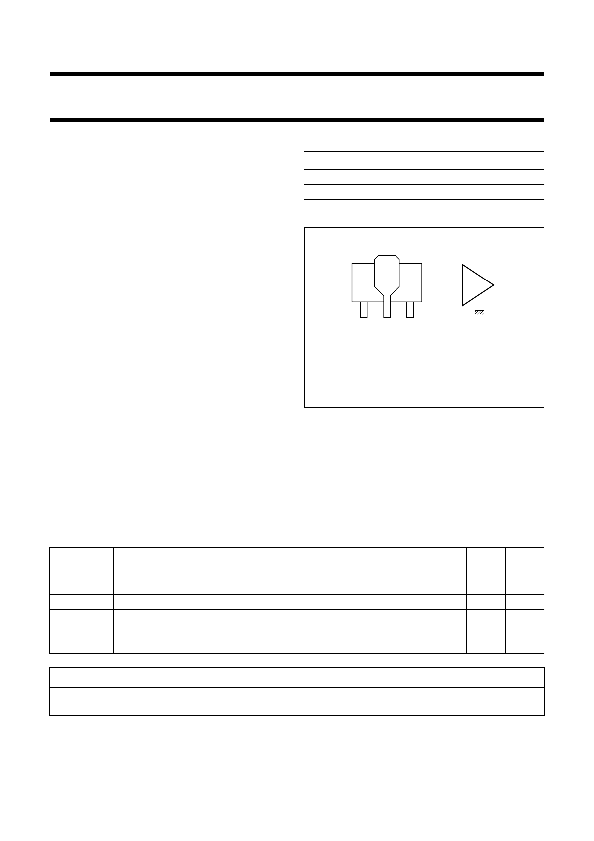
PINNING
PIN DESCRIPTION
1 RF out/bias
2 GND
3RFin
handbook, halfpage
3
1
23
Bottom view
Marking code: 5A.
Fig.1 Simplified outline (SOT89) and symbol.
1
2
MGX418
The BGA6x89 series of medium power gain blocks are
resistive feedback Darlington configured amplifiers.
Resistive feedback provides large bandwidth with high
accuracy.
QUICK REFERENCE DATA
SYMBOL PARAMETER CONDITIONS TYP. UNIT
V
S
I
S
2
|s
|
21
DC supply voltage IS=84mA 4.8 V
DC supply current VS=9V; R
=51Ω; Tj=25°C81mA
bias
insertion power gain f = 1.95 GHz 17 dB
NF noise figure f = 1.95 GHz 3.3 dB
P
L1dB
load power at 1 dB compression f = 850 MHz 21 dBm
f = 1.95 GHz 20 dBm
CAUTION
This product is supplied in anti-static packing to prevent damage caused by electrostatic discharge during transport
and handling. For further information, refer to Philips specs.: SNW-EQ-608, SNW-FQ-302A and SNW-FQ-302B.
2003 Sep 19 2
Page 3

Philips Semiconductors Product specification
MMIC wideband medium power amplifier BGA6589
LIMITING VALUES
In accordance with the Absolute Maximum Rating System (IEC 60134)
SYMBOL PARAMETER CONDITIONS MIN. MAX. UNIT
V
S
I
S
P
tot
T
stg
T
j
P
D
Note
1. T
is the temperature at the soldering point of pin 2.
s
THERMAL CHARACTERISTICS
SYMBOL PARAMETER CONDITIONS VALUE UNIT
R
th j-s
DC device voltage RF input AC coupled − 6V
DC supply current − 150 mA
total power dissipation Ts≤ 70 °C; note 1 − 800 mW
storage temperature −65 +150 °C
operating junction temperature − 150 °C
maximum drive power − 15 dBm
thermal resistance from junction to solder point Ts≤ 70 °C note 1 100 K/W
Note
is the temperature at the soldering point of pin 2.
1. T
s
STATIC CHARACTERISTICS
Tj=25°C; VS=9V; R
=51Ω; unless otherwise specified.
bias
SYMBOL PARAMETER CONDITIONS MIN. TYP. MAX. UNIT
I
S
supply current 73 81 89 mA
2003 Sep 19 3
Page 4

Philips Semiconductors Product specification
MMIC wideband medium power amplifier BGA6589
CHARACTERISTICS
VS=9V; IS= 84 mA; T
Z
= 50 Ω; unless otherwise specified.
L=ZS
SYMBOL PARAMETER CONDITIONS TYP. UNIT
2
|s
R
R
|
21
LIN
L OUT
insertion power gain f = 850 MHz 22 dB
return losses input f = 850 MHz 9 dB
return losses output f = 850 MHz 10 dB
NF noise figure f = 850 MHz 3.0 dB
K stability factor f = 850 MHz 1.1 −
P
L1dB
IP3
IP3
(in)
(out)
load power at 1 dB gain compression; f = 850 MHz 21 dBm
input intercept point f = 850 MHz 11 dBm
output intercept point f = 850 MHz 33 dBm
=25°C; IP3
amb
tone spacing = 1 MHz; PL= 0 dBm per tone (see Fig.2); R
(out)
f = 1.95 GHz 17 dB
f = 2.5 GHz 15 dB
f = 1.95 GHz 11 dB
f = 2.5 GHz 15 dB
f = 1.95 GHz 13 dB
f = 2.5 GHz 13 dB
f = 1.95 GHz 3.3 dB
f = 2.5 GHz 3.4 dB
f = 2.5 GHz 1.1 −
at 1 dB gain compression; f = 1.95 GHz 20 dBm
f = 2.5 GHz 15 dBm
f = 2.5 GHz 30 dBm
bias
=51Ω;
2003 Sep 19 4
Page 5

Philips Semiconductors Product specification
MMIC wideband medium power amplifier BGA6589
APPLICATION INFORMATION
Figure 2 shows a typical application circuit for the BGA6589 MMIC. The device is internally matched to 50 Ω, and
therefore does not require any external matching. The value of the input and output DC blocking capacitors C1 and C2
depends on the operating frequency; see the tables below. Capacitors C1 and C2 are used in conjunction with L1 and
C3 to fine tune the input and output impedance. For optimum supply decoupling, a 1 µF capacitor (C5) can be added.
The external components should be placed as close as possible to the MMIC. When using via holes, use multiple via
holes per pin in order to limit ground path induction. Resistor R1 is a bias resistor providing DC current stability with
temperature.
(2)
handbook, full pagewidth
50 Ω
microstrip
L1
C1 C2
3
V
D
1
C3
C4 C5
50 Ω
microstrip
R1
V
(1)
S
2
MGX419
(1) Optional capacitor for optimum supply decoupling.
(2) R1 values at operating supply voltage:
VS= 6 V; R1 = 15 Ω.
VS= 9 V; R1 = 51 Ω.
VS= 11.5 V; R1 = 82 Ω.
Fig.2 Typical application circuit.
Table 1 Component descriptions (see Fig.2)
VALUE AT OPERATING FREQUENCY
COMPONENT DESCRIPTION DIMENSIONS
500
MHz
800
MHz
1950
MHz
2400
MHz
3500
MHz
C1, C2 multilayer ceramic chip capacitor 0603 220pF 100 pF 68 pF 56 pF 39 pF
C3 multilayer ceramic chip capacitor 0603 1 nF 1 nF 1 nF 1 nF 1 nF
C4 multilayer ceramic chip capacitor 0603 100 pF 68 pF 22 pF 22 pF 15 pF
C5 (optional) electrolytic or tantalum capacitor 0603 1µF1µF1µF1µF1µF
L1 SMD inductor 0603 68 nH 33 nH 22 nH 18 nH 15 nH
R1 SMD resistor 0.5 W; V
=9V − −−−−−
S
2003 Sep 19 5
Page 6

Philips Semiconductors Product specification
MMIC wideband medium power amplifier BGA6589
handbook, full pagewidth
180°
IS= 84 mA; VS= 9 V; PD= −30 dBm; ZO=50Ω.
90°
+1
+0.5
+0.2
0
−0.2
0.50.2
2.6 GHz
−0.5
1
−1
−90°
2
200 MHz
+2
−2
45°135°
+5
5
10
−5
−45°−135°
MGX409
Fig.3 Input reflection coefficient (s11); typical values.
1.0
0.8
0.6
0.4
0.2
0°
0
1.0
handbook, full pagewidth
180°
IS= 84 mA; VS= 9 V; PD= −30 dBm; ZO=50Ω.
Fig.4 Output reflection coefficient (s22); typical values.
90°
+1
+0.5
+0.2
0
−0.2
−0.5
2.6 GHz
0.50.2
1
−1
−90°
2
200 MHz
+2
−2
45°135°
+5
5
10
−5
−45°−135°
MGX410
1.0
0.8
0.6
0.4
0.2
0°
0
1.0
2003 Sep 19 6
Page 7

Philips Semiconductors Product specification
MMIC wideband medium power amplifier BGA6589
handbook, halfpage
0
2
|s12|
(dB)
−10
−20
−30
−40
0 1500500 2000 2500
IS= 84 mA; VS= 9 V; PD= −30 dBm; ZO=50Ω.
1000
MGX411
f (MHz)
Fig.5 Isolation (|s12|2) as a function of frequency;
typical values.
25
handbook, halfpage
2
|s21|
(dB)
20
15
10
5
0
0 1500500 2000 2500
IS= 84 mA; VS= 9 V; PD= −30 dBm; ZO=50Ω.
1000
Fig.6 Insertion gain (|s21|2) as a function of
frequency; typical values.
MGX412
f (MHz)
25
handbook, halfpage
P
L1dB
(dBm)
20
15
10
5
0
0 1500500 2000 2500
IS= 84 mA; VS= 9 V; ZO=50Ω.
1000
MGX413
f (MHz)
Fig.7 Load power as a function of frequency;
typical values.
2003 Sep 19 7
40
handbook, halfpage
IP3
(out)
(dBm)
30
20
10
0
0 1500500 2000 2500
IS= 84 mA; VS= 9 V; PL= 0 dBm; ZO=50Ω.
1000
MGX414
f (MHz)
Fig.8 Output intercept as a function of frequency;
typical values.
Page 8

Philips Semiconductors Product specification
MMIC wideband medium power amplifier BGA6589
handbook, halfpage
5
NF
(dB)
4
3
2
1
0
0 1500500 2000 2500
IS= 84 mA; VS= 9 V; ZO=50Ω.
1000
f (MHz)
Fig.9 Noise figure as a function of frequency;
typical values.
MGX415
handbook, halfpage
5
K
4
3
2
1
0
0 1500500 2000 2500
IS= 84 mA; VS= 9 V; ZO=50Ω.
1000
MGX416
f (MHz)
Fig.10 Stability factor as a function of frequency;
typical values.
100
handbook, halfpage
I
s
(mA)
90
80
70
60
−40 40−20 0 60 80
VS= 8 V; R
bias
20
=51Ω.
MGX417
Tj (°C)
Fig.11 Supply current as a function of operating
junction temperature; typical values.
2003 Sep 19 8
Page 9

This text is here in white to force landscape pages to be rotated correctly when browsing through the pdf in the Acrobat reader.This text is here in
_white to force landscape pages to be rotated correctly when browsing through the pdf in the Acrobat reader.This text is here inThis text is here in
white to force landscape pages to berotated correctly when browsingthrough the pdf inthe Acrobat reader. white to force landscape pages tobe ...
2003 Sep 19 9
2003 Sep 19 9
Scattering parameters
IS= 83 mA; VS=8V; PD=−30 dBm; ZO=50Ω; T
s
11
f (MHz)
MAGNITUDE
(ratio)
ANGLE
(deg)
MAGNITUDE
(ratio)
amb
=25°C
s
21
ANGLE
(deg)
MAGNITUDE
(ratio)
s
12
ANGLE
(deg)
MAGNITUDE
(ratio)
s
22
ANGLE
(deg)
200 0.30 −6.87 16.61 161.86 0.04 2.38 0.34 −20.03 1.0
300 0.31 −10.91 16.18 153.02 0.04 3.66 0.34 −30.50 1.0
400 0.32 −15.72 15.59 144.39 0.04 5.17 0.34 −40.74 1.1
500 0.33 −21.0 14.91 136.01 0.04 6.75 0.34 −50.56 1.1
600 0.33 −26.44 14.19 128.12 0.04 8.67 0.34 −60.07 1.1
700 0.34 −32.08 13.51 120.88 0.04 10.94 0.33 −69.21 1.1
800 0.34 −37.75 12.77 114.19 0.04 13.65 0.33 −77.91 1.1
900 0.35 −43.18 11.88 107.40 0.04 15.15 0.32 −86.13 1.1
1000 0.35 −48.9 11.22 101.34 0.04 17.89 0.32 −94.01 1.1
1100 0.35 −54.2 10.64 95.86 0.04 19.93 0.31 −101.7 1.1
1200 0.35 −59.55 10.0 90.82 0.05 22.11 0.30 -109.1 1.1
1300 0.34 −64.78 9.39 85.46 0.05 24.10 0.30 −116.4 1.1
1400 0.34 −69.93 8.93 80.15 0.05 24.62 0.29 −123.6 1.1
1500 0.33 −74.81 8.54 75.95 0.05 25.98 0.28 −130.9 1.1
1600 0.33 −79.82 8.07 72.26 0.05 27.67 0.27 −138.2 1.1
1700 0.32 −84.88 7.60 67.95 0.06 28.69 0.26 −145.7 1.1
1800 0.31 −89.81 7.32 63.43 0.06 28.33 0.25 −153.6 1.1
1900 0.30 −94.89 7.08 59.81 0.06 28.44 0.24 −162.0 1.1
2000 0.29 −100.3 6.74 56.09 0.07 29.27 0.23 −170.7 1.1
2100 0.28 −105.9 6.46 51.84 0.07 29.17 0.23 179.99 1.1
2200 0.26 −111.8 6.28 48.02 0.07 28.46 0.22 170.17 1.2
2300 0.25 −118.0 6.07 45.0 0.08 28.37 0.22 160.16 1.2
2400 0.24 −125.2 5.78 41.33 0.08 28.17 0.22 149.59 1.1
2500 0.22 −132.8 5.61 36.72 0.08 26.46 0.23 139.39 1.2
2600 0.21 −141.3 5.51 33.15 0.09 24.85 0.24 129.67 1.0
2700 0.21 −153.3 5.33 30.04 0.09 24.72 0.28 120.55 1.2
2800 0.07 −127.7 6.44 28.98 0.12 24.46 0.28 80.88 1.2
2900 0.19 −167.20 4.88 19.14 0.10 20.48 0.27 105.15 1.2
3000 0.18 178.11 4.78 16.89 0.10 19.71 0.30 96.35 1.2
3100 0.18 165.13 4.57 16.56 0.11 18.98 0.32 89.48 1.0
K-FACTOR
Philips Semiconductors Product specification
Philips Semiconductors Product specification
MMIC wideband medium power amplifier BGA6589
MMIC wideband medium power amplifier BGA6589
Page 10

Philips Semiconductors Product specification
MMIC wideband medium power amplifier BGA6589
PACKAGE OUTLINE
Plastic surface mounted package; collector pad for good heat transfer; 3 leads SOT89
w M
D
b
3
B
A
E
L
123
b
2
b
1
e
1
e
H
E
c
0 2 4 mm
scale
DIMENSIONS (mm are the original dimensions)
UNIT
A
1.6
mm
1.4
OUTLINE
VERSION
SOT89 TO-243 SC-62
b
0.48
0.35
b
2
1
0.53
0.40
IEC JEDEC EIAJ
b
1.8
1.4
c
D
3
0.44
0.37
E
4.6
2.6
4.4
2.4
REFERENCES
e
3.0
2003 Sep 19 10
e
1.5
L
H
E
1
min.
4.25
3.75
0.8
w
0.13
EUROPEAN
PROJECTION
ISSUE DATE
97-02-28
99-09-13
Page 11

Philips Semiconductors Product specification
MMIC wideband medium power amplifier BGA6589
DATA SHEET STATUS
LEVEL
DATA SHEET
STATUS
(1)
PRODUCT
STATUS
(2)(3)
DEFINITION
I Objective data Development This data sheet contains data from the objective specification for product
development. Philips Semiconductors reserves the right to change the
specification in any manner without notice.
II Preliminary data Qualification This data sheet contains data from the preliminary specification.
Supplementary data will be published at a later date. Philips
Semiconductors reserves the right to change the specification without
notice, in order to improve the design and supply the best possible
product.
III Product data Production This data sheet contains data from the product specification. Philips
Semiconductors reserves the right to make changes at any time in order
to improve the design, manufacturing and supply. Relevant changes will
be communicated via a Customer Product/Process Change Notification
(CPCN).
Notes
1. Please consult the most recently issued data sheet before initiating or completing a design.
2. The product status of the device(s) described in this data sheet may have changed since this data sheet was
published. The latest information is available on the Internet at URL http://www.semiconductors.philips.com.
3. For datasheets describingmultiple type numbers, the highest-levelproduct status determines the datasheet status.
DEFINITIONS
DISCLAIMERS
Short-form specification The data in a short-form
specification is extracted from a full data sheet with the
same type number and title. For detailed information see
the relevant data sheet or data handbook.
Limiting valuesdefinition Limiting values givenare in
accordance with the Absolute Maximum Rating System
(IEC 60134). Stress above one or more of the limiting
values may cause permanent damage to the device.
These are stress ratings only and operation of the device
atthese oratany otherconditions above thosegiven inthe
Characteristics sectionsof the specification isnot implied.
Exposure to limiting values for extended periods may
affect device reliability.
Application information Applications that are
described herein for any of these products are for
illustrative purposes only. Philips Semiconductors make
norepresentation orwarrantythat such applicationswillbe
suitable for the specified use without further testing or
modification.
Life support applications These products are not
designed for use in life support appliances, devices, or
systems where malfunction of these products can
reasonably be expected to result in personal injury. Philips
Semiconductorscustomers usingorselling these products
for use in such applications do so at their own risk and
agree to fully indemnify Philips Semiconductors for any
damages resulting from such application.
Right to make changes Philips Semiconductors
reserves the right to make changes in the products including circuits, standard cells, and/or software described or contained herein in order to improve design
and/or performance. When theproduct isin fullproduction
(status ‘Production’), relevant changes will be
communicated via a Customer Product/Process Change
Notification (CPCN). Philips Semiconductors assumes no
responsibility or liability for the use of any of these
products, conveys no licence or title under any patent,
copyright, or mask work right to these products, and
makes no representations or warranties that these
products are free from patent, copyright, or mask work
right infringement, unless otherwise specified.
2003 Sep 19 11
Page 12

Philips Semiconductors – a w orldwide compan y
Contact information
For additional information please visit http://www.semiconductors.philips.com. Fax: +31 40 27 24825
For sales offices addresses send e-mail to: sales.addresses@www.semiconductors.philips.com.
© Koninklijke Philips Electronics N.V. 2003
All rights are reserved. Reproduction in whole or in part is prohibited without the prior written consent of the copyright owner.
The information presented in this document does not form part of any quotationor contract, is believed tobe accurate and reliable and may be changed
without notice. No liability will be accepted by the publisher for any consequence of its use. Publication thereof does not convey nor imply any license
under patent- or other industrial or intellectual property rights.
Printed in The Netherlands R77/01/pp12 Date of release:2003 Sep 19 Document order number: 9397 75011765
SCA75
 Loading...