

Page 1
BGA6489
MMIC wideband medium power amplifier
Rev. 02 — 15 June 2009 Product data sheet
1. Product profile
1.1 General description
The BGA6489 is a silicon Monolithic Microwave Integrated Circuit (MMIC) wideband
medium power amplifier with internal matching circuit in a 3-pin SOT89 plastic, low
thermal resistance, SMD package.
The BGA6x89 series of medium power gain blocks are resistive feedback Darlington
configured amplifiers. Resistive feedback provides large bandwidth with high accuracy.
CAUTION
This device is sensitive to ElectroStatic Discharge (ESD). Therefore care should be taken
during transport and handling.
1.2 Features
n Broadband 50 Ω gain block
n 20 dBm output power
n SOT89 package
n Single supply voltage needed
1.3 Applications
n Broadband medium power gain blocks
n Small signal high linearity amplifiers
n Variable gain and high output power in combination with the BGA2031
n Cellular, PCS and CDPD
n IF/RF buffer amplifier
n Wireless data SONET
n Oscillator amplifier, final PA
n Drivers for CATV amplifier
Page 2
NXP Semiconductors
1.4 Quick reference data
Table 1. Quick reference data
Symbol Parameter Conditions Min Typ Max Unit
V
D
I
S
|
|s
21
NF noise figure f = 1950 MHz - 3.3 - dB
P
L1dB
DC device voltage on pin 1; IS = 78 mA - 5.1 - V
DC supply current VS = 8 V; R1 = 39 Ω;
2
insertion power gain f = 1950 MHz - 16 - dB
load power at 1 dB
gain compression
2. Pinning information
Table 2. Pinning
Pin Description Simplified outline Graphic symbol
1 RF_OUT/BIAS
2 GND
3 RF_IN
BGA6489
MMIC wideband medium power amplifier
-78-mA
T
=25°C
j
f = 850 MHz - 20 - dBm
f = 1950 MHz - 17 - dBm
13
2
3. Ordering information
Table 3. Ordering information
Type number Package
BGA6489 SC-62 plastic surface-mounted package; collector pad for
4. Marking
Table 4. Marking codes
Type number Marking code
BGA6489 4A
321
Name Description Version
good heat transfer; 3 leads
sym130
SOT89
BGA6489_2 © NXP B.V. 2009. All rights reserved.
Product data sheet Rev. 02 — 15 June 2009 2 of 13
Page 3

NXP Semiconductors
5. Limiting values
Table 5. Limiting values
In accordance with the Absolute Maximum Rating System (IEC 60134).
Symbol Parameter Conditions Min Max Unit
V
D
I
S
P
tot
T
stg
T
j
P
D
[1] Tsp is the temperature at the solder point of the ground lead, pin 2.
DC device voltage on pin 1; RF input AC coupled - 6 V
DC supply current - 150 mA
total power dissipation Tsp≤ 70 °C
storage temperature −65 +150 °C
junction temperature - 150 °C
maximum drive power - 15 dBm
6. Thermal characteristics
Table 6. Thermal characteristics
Symbol Parameter Conditions Typ Unit
R
th(j-sp)
[1] Tsp is the temperature at the solder point of the ground lead, pin 2.
thermal resistance from junction to solder point Tsp≤ 70 °C
BGA6489
MMIC wideband medium power amplifier
[1]
- 800 mW
[1]
100 K/W
7. Characteristics
Table 7. Static characteristics
VS = 8 V; Tj = 25°C; R
Symbol Parameter Conditions Min Typ Max Unit
V
D
I
S
[1] VS= DC operating supply voltage applied to R
Table 8. Characteristics
VS=8V;IS= 78 mA; T
Z
L=ZS
Symbol Parameter Conditions Min Typ Max Unit
2
|
|s
21
R
LIN
R
LOUT
[1]
=39
bias
Ω
DC device voltage on pin 1; IS=78mA - 5.1 - V
supply current 70 78 86 mA
; see Figure10
bias
=25°C; IP3
amb
tone spacing = 1 MHz; PL= 0 dB per tone,R
(out)
bias
=50Ω; unless otherwise specified; see Figure 10.
Insertion power gain f = 850 MHz - 20 - dB
f = 1950 MHz - 16 - dB
f = 2500 MHz - 15 - dB
return losses input f = 850 MHz - 14 - dB
f = 1950 MHz - 16 - dB
f = 2500 MHz - 19 - dB
return losses output f = 850 MHz - 16 - dB
f = 1950 MHz - 12 - dB
f = 2500 MHz - 10 - dB
=39Ω;
BGA6489_2 © NXP B.V. 2009. All rights reserved.
Product data sheet Rev. 02 — 15 June 2009 3 of 13
Page 4
NXP Semiconductors
BGA6489
MMIC wideband medium power amplifier
Table 8. Characteristics
VS=8V;IS= 78 mA; T
Z
=50Ω; unless otherwise specified; see Figure 10.
L=ZS
…continued
=25°C; IP3
amb
tone spacing = 1 MHz; PL= 0 dB per tone,R
(out)
bias
=39Ω;
Symbol Parameter Conditions Min Typ Max Unit
NF noise figure f = 850 MHz - 3.1 - dB
f = 1950 MHz - 3.3 - dB
f = 2500 MHz - 3.4 - dB
K stability factor f = 850 MHz - 1.2 -
f = 2500 MHz - 1.3 -
P
L1dB
load power at 1 dB gain compression f = 850 MHz - 20 - dBm
f = 1950 MHz - 17 - dBm
IP3
input intercept point f = 850 MHz - 13 - dBm
(in)
f = 2500 MHz - 12 - dBm
IP3
output intercept point f = 850 MHz - 33 - dBm
(out)
f = 2500 MHz - 27 - dBm
+0.5
90°
+1
+2
45°135°
1.0
0.8
0.6
+0.2
0
180°
−0.2
IS = 78 mA; VS = 8 V; PD = −30 dBm; ZO = 50 Ω.
0.50.2
2.6 GHz
−0.5
200 MHz
−1
−90°
2
Fig 1. Input reflection coefficient (s11); typical values
−2
+5
5
10
−5
−45°−135°
mgx400
0.4
0.2
0°
0
1.0
BGA6489_2 © NXP B.V. 2009. All rights reserved.
Product data sheet Rev. 02 — 15 June 2009 4 of 13
Page 5
NXP Semiconductors
BGA6489
MMIC wideband medium power amplifier
90°
+1
+0.5
180°
+0.2
0
−0.2
−0.5
2.6 GHz
0.50.2
1
−1
−90°
2
200 MHz
IS = 78 mA; VS = 8 V; PD = −30 dBm; ZO = 50 Ω.
Fig 2. Output reflection coefficient (s22); typical values
+2
−2
1.0
45°135°
+5
5
10
−5
−45°−135°
mgx401
0.8
0.6
0.4
0.2
0°
0
1.0
25
2
|s21|
(dB)
20
15
10
5
0
0 1500500 2000 2500
1000
mgx403
f (MHz)
IS = 78 mA; VS = 8 V; PD = −30 dBm; ZO = 50 Ω.I
Fig 3. Insertion power gain (|s21|2) as a function of
frequency; typical values
0
2
|s12|
(dB)
−10
−20
−30
−40
0 1500500 2000 2500
= 78 mA; VS = 8 V; PD = −30 dBm; ZO = 50 Ω.
S
1000
mgx402
f (MHz)
Fig 4. Isolation (|s12|2) as a function of frequency;
typical values
BGA6489_2 © NXP B.V. 2009. All rights reserved.
Product data sheet Rev. 02 — 15 June 2009 5 of 13
Page 6
NXP Semiconductors
BGA6489
MMIC wideband medium power amplifier
25
P
L1dB
(dBm)
20
15
10
5
0
0 1500500 2000 2500
1000
mgx404
f (MHz)
IS = 78 mA; VS = 8 V; ZO = 50 Ω.I
Fig 5. Load power as a function of frequency; typical
values
5
K
4
mgx407
40
IP3
(out)
(dBm)
30
20
10
0
0 1500500 2000 2500
= 78 mA; VS = 8 V; ZO = 50 Ω.
S
1000
mgx405
f (MHz)
Fig 6. Output intercept as a function of frequency;
typical values
mgx406
NF
(dB)
5
4
3
2
1
0
0 1500500 2000 2500
1000
f (MHz)
IS = 78 mA; VS = 8 V; ZO = 50 Ω.I
Fig 7. Stability factor as a function of frequency;
typical values
3
2
1
0
0 1500500 2000 2500
= 78 mA; VS = 8 V; ZO = 50 Ω.
S
1000
f (MHz)
Fig 8. Noise figure as a functionof frequency; typical
values
BGA6489_2 © NXP B.V. 2009. All rights reserved.
Product data sheet Rev. 02 — 15 June 2009 6 of 13
Page 7
NXP Semiconductors
BGA6489
MMIC wideband medium power amplifier
VS = 8 V; R
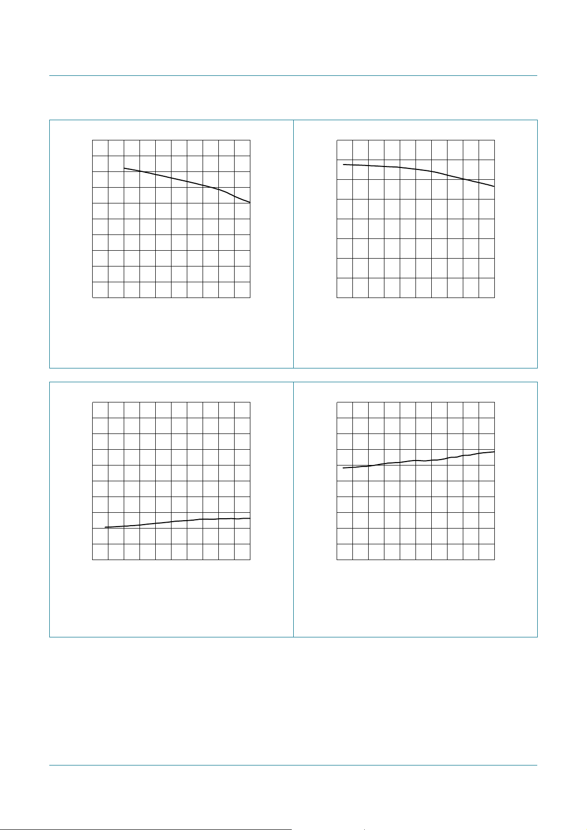
Fig 9. Supply current as function of operating junction temperature; typical values
8. Application information
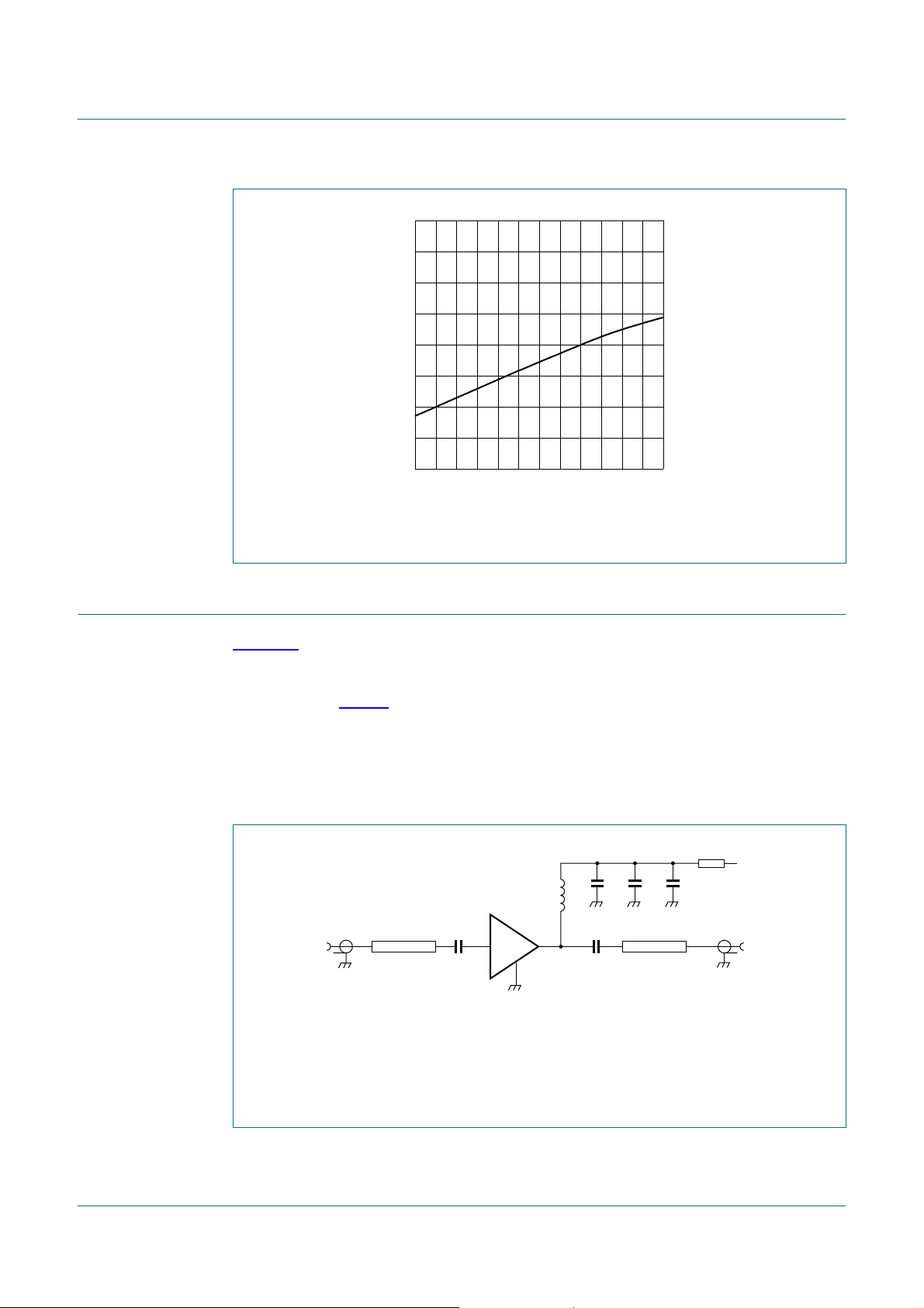
Figure 10 shows a typical application circuit for the BGA6489 MMIC. The device is
internally matched to 50 Ω and therefore does not require any external matching. The
value of the input andoutput DC blockingcapacitors C1 and C2 depends on the operating
frequency; see Table 9. Capacitors C1 and C2 are used in conjunction with L1 and C3 to
fine tune the input and output impedance. Capacitor C4 is a supply decoupling capacitor.
A1µF capacitor (C5) can be added for optimum supply decoupling. The external
components should be placed as close as possible to the MMIC. When using via holes,
use multiple via holes per pin in order to limit ground path induction. Resistor R1 is a bias
resistor providing DC current stability with temperature.
100
I
s
(mA)
90
80
70
60
−40 40−20 0 60 80
=39Ω.
bias
20
mgx408
(°C)
T
j
(2)
R1
V
S
mgx419
50 Ω
microstrip
L1
C1 C2
3
2
V
D
1
C3
C4 C5
50 Ω
microstrip
(1)
(1) Optional capacitor for optimum supply decoupling.
(2) R1 values at operating supply voltage:
VS = 6 V; R1 = 27 Ω.
VS = 8 V; R1 = 39 Ω.
VS = 11 V; R1 = 82 Ω.
Fig 10. Typical application circuit
BGA6489_2 © NXP B.V. 2009. All rights reserved.
Product data sheet Rev. 02 — 15 June 2009 7 of 13
Page 8

NXP Semiconductors
BGA6489
MMIC wideband medium power amplifier
Table 9. List of components
See Figure 10 for circuit.
Component Description Package Value at operating frequency
500 MHz 800 MHz 1950 MHz 2400 MHz 3500 MHz
C1, C2 multilayer ceramic chip capacitor 0603 220 pF 100 pF 68 pF 56 pF 39 pF
C3 multilayer ceramic chip capacitor 0603 100 pF 68 pF 22 pF 22 pF 15 pF
C4 multilayer ceramic chip capacitor 0603 1 nF 1 nF 1 nF 1 nF 1 nF
C5
[1]
electrolytic or tantalum capacitor 0603 1 µF1µF1µF1µF1µF
L1 SMD inductor 0603 68 nH 33 nH 22 nH 18 nH 15 nH
R1 SMD resistor 0.5W; V
[1] Optional.
= 8 V - 39 Ω 39 Ω 39 Ω 39 Ω 39Ω
S
8.1 Scattering parameters
Table 10. Scattering parameters
IS = 78 mA; VS=8V; PD =−30 dBm; ZO=50Ω; T
f (MHz) s
11
Magnitude
(ratio)
Angle
(degree)
s
21
Magnitude
(ratio)
200 0.06 28.11 12.79 164.42 0.06 −0.30 0.12 −22.91 1.1
300 0.09 27.41 12.59 156.85 0.06 −0.39 0.13 −35.38 1.1
400 0.11 21.64 12.31 149.28 0.06 −0.35 0.14 −46.54 1.1
500 0.12 15.28 11.97 141.88 0.06 −0.32 0.14 −57.20 1.1
600 0.14 8.01 11.57 134.79 0.06 0.04 0.15 −61.41 1.1
700 0.16 0.34 11.18 127.97 0.06 0.63 0.16 −76.76 1.1
800 0.17 −7.27 10.75 121.56 0.05 1.57 0.16 −85.75 1.2
900 0.18 −14.78 10.24 115.06 0.05 1.85 0.17 −94.28 1.2
1000 0.19 −22.18 9.80 109.18 0.05 3.16 0.17 −102.4 1.2
1100 0.20 −29.33 9.40 103.40 0.05 4.29 0.17 −110.3 1.2
1200 0.21 −36.41 8.96 98.12 0.05 5.64 0.17 −118.5 1.2
1300 0.21 −42.47 8.53 92.76 0.05 7.03 0.17 −126.7 1.2
1400 0.22 −49.06 8.16 87.50 0.06 7.74 0.17 −134.8 1.2
1500 0.22 −55.46 7.85 82.76 0.06 9.08 0.17 −143.5 1.3
1600 0.22 −61.20 7.51 78.52 0.06 10.76 0.16 −152.7 1.3
1700 0.22 −67.02 7.16 74.16 0.06 11.89 0.16 −161.8 1.3
1800 0.21 −73.40 6.90 69.37 0.06 12.34 0.16 −171.9 1.3
1900 0.21 −78.99 6.69 65.14 0.06 13.16 0.16 177.4 1.3
2000 0.20 −84.54 6.42 61.15 0.06 14.33 0.16 166.81 1.3
2100 0.19 −91.32 6.16 56.80 0.07 14.84 0.17 156.07 1.3
2200 0.18 −97.58 5.99 52.55 0.07 15.05 0.17 145.29 1.3
2300 0.17 −103.60 5.83 49.08 0.07 15.72 0.19 135.65 1.3
2400 0.16 −111.90 5.58 45.43 0.07 15.96 0.20 126.23 1.3
2500 0.14 −120.80 5.39 40.67 0.08 15.27 0.22 117.16 1.3
2600 0.13 −129.80 5.30 36.66 0.08 14.68 0.24 110.35 1.3
=25°C
amb
Angle
(degree)
s
12
Magnitude
(ratio)
Angle
(degree)
s
22
Magnitude
(ratio)
K
Angle
(degree)
BGA6489_2 © NXP B.V. 2009. All rights reserved.
Product data sheet Rev. 02 — 15 June 2009 8 of 13
Page 9

NXP Semiconductors
BGA6489
MMIC wideband medium power amplifier
Table 10. Scattering parameters
IS = 78 mA; VS=8V; PD =−30 dBm; ZO=50Ω; T
f (MHz) s
11
Magnitude
(ratio)
Angle
(degree)
s
21
Magnitude
(ratio)
2700 0.13 −143.80 5.18 33.88 0.08 15.64 0.28 104.05 1.3
2800 0.12 −154.47 5.08 30.28 0.08 15.56 0.31 97.10 1.3
2900 0.11 −164.40 4.71 22.43 0.09 11.60 0.28 91.75 1.3
3000 0.11 178.65 4.66 18.90 0.09 11.05 0.31 84.80 1.3
3100 0.12 160.01 4.45 18.63 0.10 10.63 0.33 80.37 1.3
=25°C
amb
Angle
(degree)
s
12
Magnitude
(ratio)
Angle
(degree)
s
22
Magnitude
(ratio)
K
Angle
(degree)
BGA6489_2 © NXP B.V. 2009. All rights reserved.
Product data sheet Rev. 02 — 15 June 2009 9 of 13
Page 10

NXP Semiconductors
BGA6489
MMIC wideband medium power amplifier
9. Package outline
Plastic surface-mounted package; collector pad for good heat transfer; 3 leads SOT89
w M
D
b
p3
123
b
p2
B
b
p1
e
1
e
B
A
E
L
p
H
E
c
0 2 4 mm
scale
DIMENSIONS (mm are the original dimensions)
UNIT
A
1.6
mm
1.4
OUTLINE
VERSION
SOT89 TO-243 SC-62
b
p1
0.48
0.35
b
p2
0.53
0.40
IEC JEDEC JEITA
b
1.8
1.4
c
D
E
2.6
2.4
e
3.0
p3
0.44
4.6
0.23
4.4
REFERENCES
e
1.5
H
L
1.2
0.8
w
p
0.13
EUROPEAN
PROJECTION
ISSUE DATE
06-03-16
06-08-29
E
1
4.25
3.75
Fig 11. Package outline SOT89 (SC-62)
BGA6489_2 © NXP B.V. 2009. All rights reserved.
Product data sheet Rev. 02 — 15 June 2009 10 of 13
Page 11

NXP Semiconductors
MMIC wideband medium power amplifier
BGA6489
10. Abbreviations
Table 11. Abbreviations
Acronym Description
CDPD Cellular Digital Packet Data
IF Intermediate Frequency
PCS Personal Communication Service
SMD Surface Mount Device
SONET Synchronous Optical NETwork
11. Revision history
Table 12. Revision history
Document ID Release date Data sheet status Change notice Supersedes
BGA6489_2 20090615 Product data sheet - BGA6489_1
Modifications:
BGA6489_1 20030918 Product data sheet - -
• The format of this data sheet has been redesigned to comply with the new identity
guidelines of NXP Semiconductors.
• Legal texts have been adapted to the new company name where appropriate.
• Changed I
• Table 1: changed symbol V
• Table 5: changed symbol V
• Table 7: added row for V
from 74 mA to 78 mA throughout.
S
to VD.
S
to VD and added “on pin 1;” to Conditions.
S
DC device voltage.
D
• Section 8: added sentence.
• Table 9: added 39 Ω to all value columns for resistor R1.
• Table 9: amended values of C3 and C4.
BGA6489_2 © NXP B.V. 2009. All rights reserved.
Product data sheet Rev. 02 — 15 June 2009 11 of 13
Page 12

NXP Semiconductors
12. Legal information
12.1 Data sheet status
BGA6489
MMIC wideband medium power amplifier
Document status
Objective [short] data sheet Development This document contains data from the objective specification for product development.
Preliminary [short] data sheet Qualification This document contains data from the preliminary specification.
Product [short] data sheet Production This document contains the product specification.
[1] Please consult the most recently issued document before initiating or completing a design.
[2] The term ‘short data sheet’ is explained in section “Definitions”.
[3] The product status of device(s) described in this document may have changed since this document was published and may differ in case of multiple devices. The latest product status
information is available on the Internet at URL
[1][2]
Product status
12.2 Definitions
Draft — The document is a draft version only. The content is still under
internal review and subject to formal approval, which may result in
modifications or additions. NXP Semiconductors does not give any
representations or warranties as to the accuracy or completeness of
information included herein and shall haveno liability for the consequences of
use of such information.
Short data sheet — A short data sheet is an extract from a full data sheet
with the same product type number(s) and title.A short data sheet is intended
for quick referenceonly andshould notbe reliedupon tocontain detailed and
full information. For detailed and full information see the relevant full data
sheet, which is available on request via the local NXP Semiconductors sales
office. In case of any inconsistency or conflict with the short data sheet, the
full data sheet shall prevail.
12.3 Disclaimers
General — Information in this document is believed to be accurate and
reliable. However,NXP Semiconductorsdoes notgive any representations or
warranties, expressed or implied, asto theaccuracy or completeness ofsuch
information and shall have no liability for the consequences of use of such
information.
Right to make changes — NXP Semiconductors reserves the right to make
changes to information published in this document, including without
limitation specifications and product descriptions, at any time and without
notice. This document supersedes and replaces allinformation supplied prior
to the publication hereof.
Suitability for use — NXP Semiconductors products are not designed,
authorized or warranted to be suitable for use in medical, military, aircraft,
space or life support equipment, nor in applications where failure or
malfunction of an NXP Semiconductors product can reasonably be expected
to result in personal injury, death or severe property or environmental
[3]
http://www.nxp.com.
Definition
damage. NXP Semiconductors accepts no liability for inclusion and/or use of
NXP Semiconductors products in such equipment or applications and
therefore such inclusion and/or use is at the customer’s own risk.
Applications — Applications that are described herein for any of these
products are for illustrative purposes only. NXP Semiconductors makes no
representation or warranty that such applications will be suitable for the
specified use without further testing or modification.
Limiting values — Stress above one or more limiting values (as defined in
the Absolute Maximum Ratings System of IEC 60134)may cause permanent
damage to the device. Limiting values are stress ratings only and operation of
the device at these or any other conditions above those given in the
Characteristics sections of this document is not implied. Exposure to limiting
values for extended periods may affect device reliability.
Terms and conditions of sale — NXP Semiconductors products are sold
subject to the general terms and conditions of commercial sale, as published
at
http://www.nxp.com/profile/terms, including those pertaining to warranty,
intellectual property rights infringement and limitation of liability, unless
explicitly otherwise agreed to in writing by NXP Semiconductors. In case of
any inconsistency or conflict between information in this document and such
terms and conditions, the latter will prevail.
No offer to sell or license — Nothing in this document may be interpreted
or construed as an offer to sell products that is open for acceptance or the
grant, conveyanceor implication of any license under any copyrights, patents
or other industrial or intellectual property rights.
Export control — This document as well as the item(s) described herein
may be subject to export control regulations. Export might require a prior
authorization from national authorities.
Quick reference data — The Quick reference data is an extract of the
product data given in the Limiting values and Characteristics sections of this
document, and as such is not complete, exhaustive or legally binding.
12.4 Trademarks
Notice: All referencedbrands, product names, service names and trademarks
are the property of their respective owners.
13. Contact information
For more information, please visit: http://www.nxp.com
For sales office addresses, please send an email to: salesaddresses@nxp.com
BGA6489_2 © NXP B.V. 2009. All rights reserved.
Product data sheet Rev. 02 — 15 June 2009 12 of 13
Page 13

NXP Semiconductors
14. Contents
1 Product profile . . . . . . . . . . . . . . . . . . . . . . . . . . 1
1.1 General description. . . . . . . . . . . . . . . . . . . . . . 1
1.2 Features . . . . . . . . . . . . . . . . . . . . . . . . . . . . . . 1
1.3 Applications . . . . . . . . . . . . . . . . . . . . . . . . . . . 1
1.4 Quick reference data. . . . . . . . . . . . . . . . . . . . . 2
2 Pinning information. . . . . . . . . . . . . . . . . . . . . . 2
3 Ordering information. . . . . . . . . . . . . . . . . . . . . 2
4 Marking. . . . . . . . . . . . . . . . . . . . . . . . . . . . . . . . 2
5 Limiting values. . . . . . . . . . . . . . . . . . . . . . . . . . 3
6 Thermal characteristics. . . . . . . . . . . . . . . . . . . 3
7 Characteristics. . . . . . . . . . . . . . . . . . . . . . . . . . 3
8 Application information. . . . . . . . . . . . . . . . . . . 7
8.1 Scattering parameters . . . . . . . . . . . . . . . . . . . 8
9 Package outline . . . . . . . . . . . . . . . . . . . . . . . . 10
10 Abbreviations. . . . . . . . . . . . . . . . . . . . . . . . . . 11
11 Revision history. . . . . . . . . . . . . . . . . . . . . . . . 11
12 Legal information. . . . . . . . . . . . . . . . . . . . . . . 12
12.1 Data sheet status . . . . . . . . . . . . . . . . . . . . . . 12
12.2 Definitions. . . . . . . . . . . . . . . . . . . . . . . . . . . . 12
12.3 Disclaimers. . . . . . . . . . . . . . . . . . . . . . . . . . . 12
12.4 Trademarks. . . . . . . . . . . . . . . . . . . . . . . . . . . 12
13 Contact information. . . . . . . . . . . . . . . . . . . . . 12
14 Contents . . . . . . . . . . . . . . . . . . . . . . . . . . . . . . 13
BGA6489
MMIC wideband medium power amplifier
Please be aware that important notices concerning this document and the product(s)
described herein, have been included in section ‘Legal information’.
© NXP B.V. 2009. All rights reserved.
For more information, please visit: http://www.nxp.com
For sales office addresses, please send an email to: salesaddresses@nxp.com
Date of release: 15 June 2009
Document identifier: BGA6489_2
 Loading...