

Philips BGA6289 Technical data

查询BGA6289供应商
DISCRETE SEMICONDUCTORS
DATA SH EET
ook, halfpage
M3D109
BGA6289
MMIC wideband medium power
amplifier
Product specification 2003 Sep 18
Philips Semiconductors Product specification
MMIC wideband medium power amplifier BGA6289
FEATURES
• Broadband 50 Ω gain block
• 17 dBm output power
• SOT89 package
• Single supply voltage needed.
APPLICATIONS
• Broadband medium power gain blocks
• Small signal high linearity amplifiers
• Variable gainand high output power in combination with
the BGA2031
• Cellular, PCS and CDPD
• IF/RF buffer amplifier
• Wireless data SONET
• Oscillator amplifier, final PA
• Drivers for CATV amplifier.
DESCRIPTION
Silicon Monolithic Microwave Integrated Circuit (MMIC)
wideband medium power amplifier with internal matching
circuit in a 4-pin SOT89 plastic low thermal resistance
SMD package.
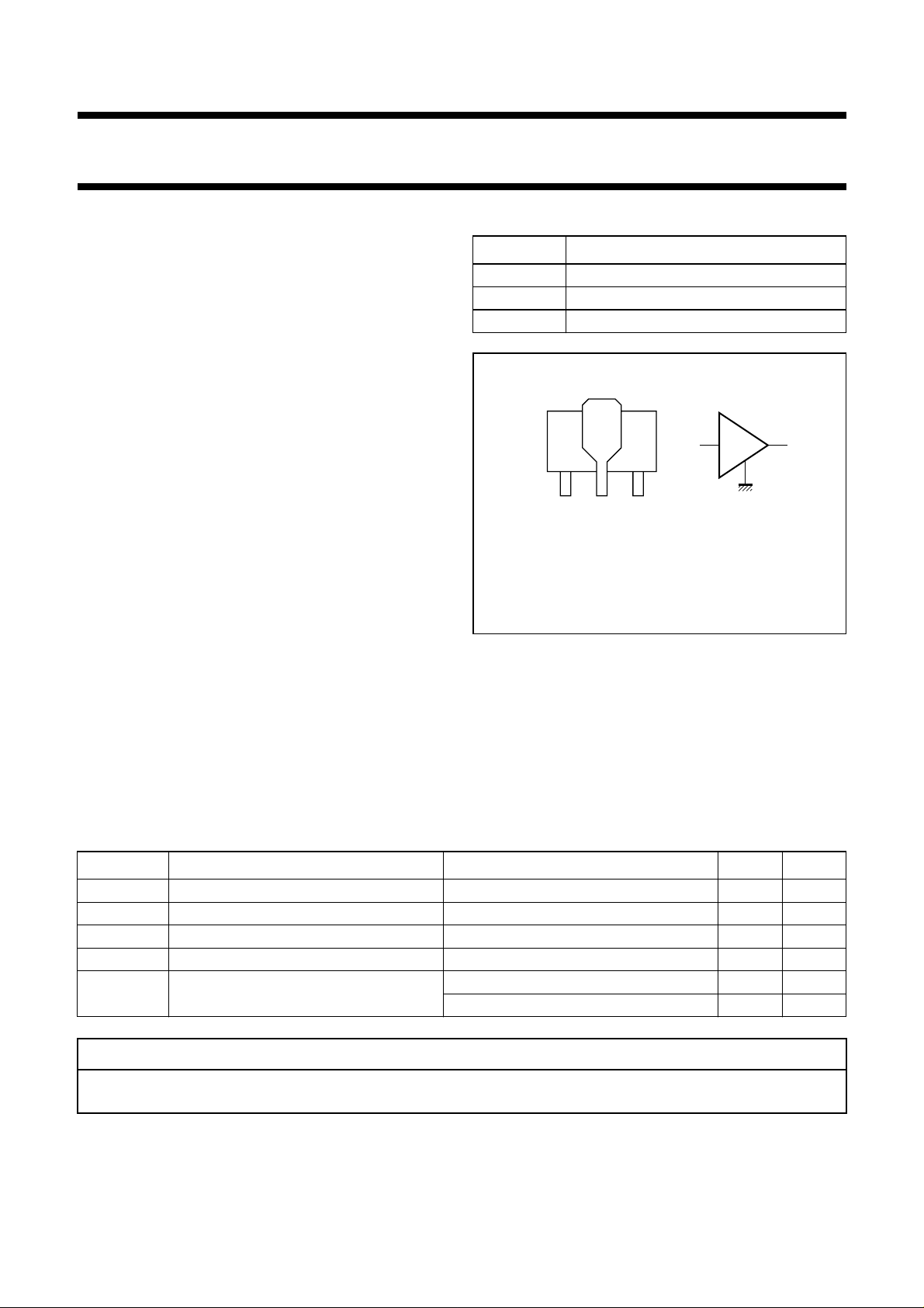
PINNING
PIN DESCRIPTION
1 RF out/bias
2 GND
3RFin
handbook, halfpage
3
1
23
Bottom view
Marking code: 3A.
Fig.1 Simplified outline (SOT89) and symbol.
1
2
MGX418
The BGA6x89 series of medium power gain blocks are
resistive feedback Darlington configured amplifiers.
Resistive feedback provides large bandwidth with high
accuracy.
QUICK REFERENCE DATA
SYMBOL PARAMETER CONDITIONS TYP. UNIT
V
S
I
S
2
|s
|
21
DC supply voltage IS= 84 mA 4.1 V
DC supply current VS= 8 V; R1 = 47 Ω; Tj=25°C88mA
insertion power gain f = 1.95 GHz 13 dB
NF noise figure f = 1.95 GHz 4 dB
P
L1dB
load power at 1 dB compression f = 850 MHz 18 dBm
f = 1.95 GHz 16 dBm
CAUTION
This product is supplied in anti-static packing to prevent damage caused by electrostatic discharge during transport
and handling. For further information, refer to Philips specs.: SNW-EQ-608, SNW-FQ-302A and SNW-FQ-302B.
2003 Sep 18 2

Philips Semiconductors Product specification
MMIC wideband medium power amplifier BGA6289
LIMITING VALUES
In accordance with the Absolute Maximum Rating System (IEC 60134)
SYMBOL PARAMETER CONDITIONS MIN. MAX. UNIT
V
S
I
S
P
tot
T
stg
T
j
P
D
Note
1. T
is the temperature at the soldering point of pin 2.
s
THERMAL CHARACTERISTICS
SYMBOL PARAMETER CONDITIONS VALUE UNIT
R
th j-s
DC supply voltage RF input AC coupled − 6V
DC supply current − 150 mA
total power dissipation Ts≤ 70 °C; note 1 − 800 mW
storage temperature −65 +150 °C
operating junction temperature − 150 °C
maximum drive power − 15 dBm
thermal resistance from junction to
Ts≤ 70 °C; note 1 100 K/W
solder point
Note
is the temperature at the soldering point of pin 2.
1. T
s
STATIC CHARACTERISTICS
Tj=25°C; VS= 8 V; R1 = 47 Ω; unless otherwise specified.
SYMBOL PARAMETER CONDITIONS MIN. TYP. MAX. UNIT
I
S
supply current 79 88 96 mA
2003 Sep 18 3

Philips Semiconductors Product specification
MMIC wideband medium power amplifier BGA6289
CHARACTERISTICS
VS=8V; IS= 84 mA; T
Z
= 50 Ω; unless otherwise specified.
L=ZS
SYMBOL PARAMETER CONDITIONS TYP. UNIT
2
|s
R
R
|
21
LIN
L OUT
insertion power gain f = 850 MHz 15 dB
return losses input f = 850 MHz 11 dB
return losses output f = 850 MHz 11 dB
NF noise figure f = 850 MHz 3.5 dB
K stability factor f = 850 MHz 1.3 −
P
L 1 dB
IP3
IP3
(in)
(out)
load power at 1 dB gain compression; f = 850 MHz 17 dBm
input intercept point f = 850 MHz 17 dBm
output intercept point f = 850 MHz 31 dBm
=25°C; IP3
amb
tone spacing = 1 MHz; PL= 0 dBm per tone (see Fig.2); R1 = 47 Ω;
(out)
f = 1.95 GHz 13 dB
f = 2.5 GHz 12 dB
f = 1.95 GHz 11 dB
f = 2.5 GHz 14 dB
f = 1.95 GHz 14 dB
f = 2.5 GHz 14 dB
f = 1.95 GHz 3.7 dB
f = 2.5 GHz 3.8 dB
f = 2.5 GHz 1.6 −
at 1 dB gain compression; f = 1.95 GHz 15 dBm
f = 2.5 GHz 14 dBm
f = 2.5 GHz 25 dBm
2003 Sep 18 4
 Loading...