

Philips BGA2776 Technical data

查询BGA2776供应商查询BGA2776供应商
DISCRETE SEMICONDUCTORS
DATA SH EET
ook, halfpage
MBD128
BGA2776
MMIC wideband amplifier
Product specification
Supersedes data of 2001 Oct 19
2002 Aug 06
Philips Semiconductors Product specification
MMIC wideband amplifier BGA2776
FEATURES
• Internally matched
• Very wide frequency range
• Very flat gain
• High gain
• High output power
• Unconditionally stable.
APPLICATIONS
• Cable systems
• LNB IF amplifiers
• General purpose
• ISM.
DESCRIPTION
Silicon Monolithic Microwave Integrated Circuit (MMIC)
wideband amplifierwith internal matching circuit in a 6-pin
SOT363 SMD plastic package.
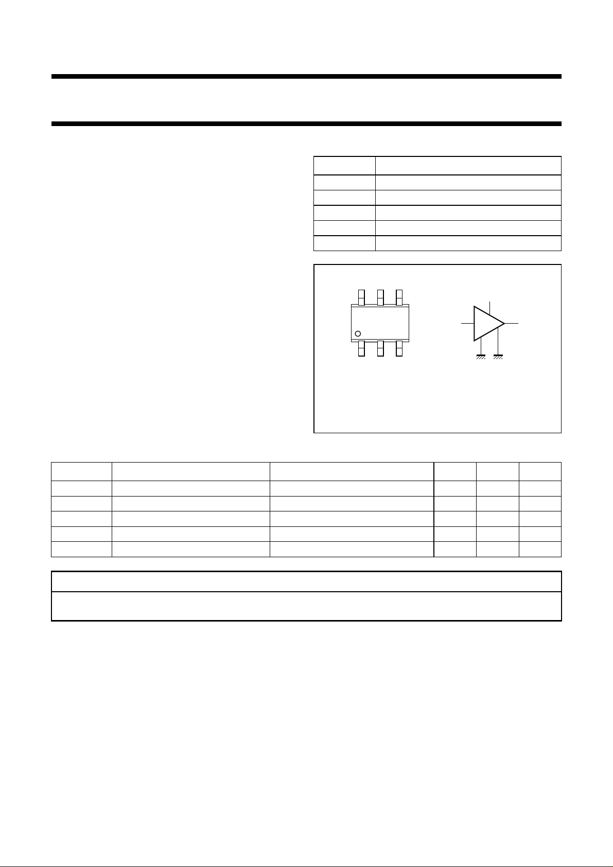
PINNING
PIN DESCRIPTION
1V
S
2, 5 GND2
3 RF out
4 GND1
6RFin
56
4
63
132
Top view
Marking code: G4-.
MAM455
Fig.1 Simplified outline (SOT363) and symbol.
1
2, 54
QUICK REFERENCE DATA
SYMBOL PARAMETER CONDITIONS TYP. MAX. UNIT
V
I
s
S
S
2
21
DC supply voltage 5 6 V
DC supply current 24.4 − mA
insertion power gain f = 1 GHz 23.2 − dB
NF noise figure f = 1 GHz 4.9 − dB
P
L(sat)
saturated load power f = 1 GHz 10.5 − dBm
CAUTION
This product is supplied in anti-static packing to prevent damage caused by electrostatic discharge during transport
and handling. For further information, refer to Philips specs.: SNW-EQ-608, SNW-FQ-302A and SNW-FQ-302B.
2002 Aug 06 2
Philips Semiconductors Product specification
MMIC wideband amplifier BGA2776
LIMITING VALUES
In accordance with the Absolute Maximum Rating System (IEC 60134).
SYMBOL PARAMETER CONDITIONS MIN. MAX. UNIT
V
S
I
S
P
tot
T
stg
T
j
P
D
THERMAL CHARACTERISTICS
SYMBOL PARAMETER CONDITIONS VALUE UNIT
R
th j-s
DC supply voltage RF input AC coupled − 6V
supply current − 34 mA
total power dissipation Ts≤ 80 °C − 200 mW
storage temperature −65 +150 °C
operating junction temperature − 150 °C
maximum drive power − 10 dBm
thermal resistance from junction to
P
= 200 mW; Ts≤ 80 °C 300 K/W
tot
solder point
CHARACTERISTICS
VS=5V; IS= 24.4 mA; f = 1 GHz; Tj=25°C; unless otherwise specified.
SYMBOL PARAMETER CONDITIONS MIN. TYP. MAX. UNIT
I
s
S
2
21
supply current 19 24.4 34 mA
insertion power gain f = 1 GHz − 23.2 − dB
f = 2 GHz − 23.2 − dB
R
LIN
return losses input f = 1 GHz − 9 − dB
f = 2 GHz − 7 − dB
R
L OUT
return losses output f = 1 GHz − 17 − dB
f = 2 GHz − 9 − dB
NF noise figure f = 1 GHz − 4.9 − dB
f = 2 GHz − 5.3 − dB
BW bandwidth at s
P
L(sat)
saturated load power f = 1 GHz − 10.5 − dBm
2−3 dB below flat gain at 1 GHz − 2.8 − GHz
21
f = 2 GHz − 8.1 − dBm
P
L 1 dB
load power at 1 dB gain compression; f = 1 GHz − 7.2 − dBm
at 1 dB gain compression; f = 2 GHz − 6 − dBm
IP3
(in)
input intercept point f = 1 GHz −−4.6 − dBm
f = 2 GHz −−8.8 − dBm
IP3
(out)
output intercept point f = 1 GHz − 18.6 − dBm
f = 2 GHz − 14.4 − dBm
2002 Aug 06 3
Philips Semiconductors Product specification
MMIC wideband amplifier BGA2776
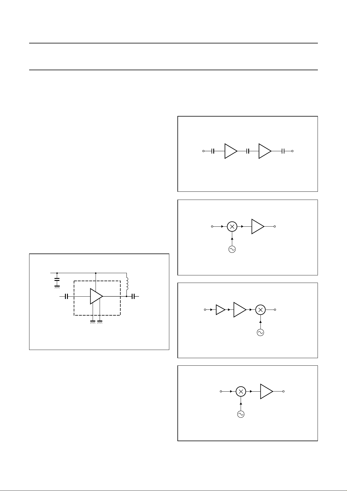
APPLICATION INFORMATION
Figure 2 shows a typical application circuit for the
BGA2776MMIC.Thedeviceisinternallymatchedto50 Ω,
and therefore does not need any external matching. The
value of the input and output DC blocking capacitors C2
and C3 should be not more than 100 pF for applications
above 100 MHz. However, when the device is operated
below 100 MHz, the capacitor value should be increased.
The nominal value of the RF choke L1 is 100 nH. At
frequencies below 100 MHz this value should be
increased to 220 nH. At frequencies above 1 GHz a much
lower value must be used (e.g. 10 nH) to improve return
losses. For optimal results, a good quality chip inductor
such as the TDK MLG 1608 (0603), or a wire-wound SMD
type should be chosen.
Both the RF choke L1 and the 22 nF supply decoupling
capacitor C1 should be located as closely as possible to
the MMIC.
Separate paths must be used for the ground planes of the
groundpinsGND1andGND2,andthesepathsmustbeas
short as possible. When using vias, use multiple vias per
pin in order to limit ground path inductance.
InFig.6theMMICisused as a driver to the power amplifier
as part of a transmitter circuit. Good linear performance
and matched input and output offer quick design solutions
in such applications.
handbook, halfpage
DC-block
100 pF
input output
DC-block
100 pF
DC-block
100 pF
MGU437
Fig.3 Simple cascade circuit.
oscillator
mixer
wideband
amplifier
to IF circuit
or demodulator
MGU438
handbook, halfpage
from RF
circuit
V
handbook, halfpage
s
RF input
C1
V
s
RF outRF in
C2 C3
GND2GND1
L1
RF output
MGU436
Fig.2 Typical application circuit.
Figure 3 shows two cascaded MMICs. This configuration
doubles overall gain while preserving broadband
characteristics. Supply decoupling and grounding
conditions for each MMIC are the same as those for the
circuit of Fig.2.
The excellent wideband characteristics of the MMIC make
it and ideal building block in IF amplifier applications such
as LBNs (see Fig.4).
As a buffer amplifier between an LNA and a mixer in a
receiver circuit, the MMIC offers an easy matching, low
noise solution (see Fig.5).
handbook, halfpage
antenna
handbook, halfpage
from modulation
or IF circuit
Fig.6 Power amplifier driver application.
Fig.4 IF amplifier application.
LNA
mixer
wideband
amplifier
oscillator
to IF circuit
or demodulator
Fig.5 RF amplifier application.
mixer
wideband
amplifier
oscillator
MGU439
to power
amplifier
MGU440
2002 Aug 06 4
 Loading...