Philips BGA2031,1 Datasheet

DATA SHEET
Preliminary specification 2000 Feb 17
DISCRETE SEMICONDUCTORS
BGA2031/1
MMIC variable gain amplifier
ook, halfpage
MBD128

2000 Feb 17 2
Philips Semiconductors Preliminary specification
MMIC variable gain amplifier BGA2031/1
FEATURES
• High gain
• Excellent adjacent channel power rejection
• Small SMD package
• Low dissipation.
APPLICATIONS
• General purpose variable gain amplifier for low voltage
and medium power
• Driver for power amplifiers in systems that require good
linearity, such as CDMA, both cellular band (850 MHz)
and PCS (1.9 GHz). This is because of the high output
power and good linearity.
DESCRIPTION
Silicon Monolitic Microwave Integrated Circuit (MMIC)
2 stage variable gain amplifier in double polysilicon
technology in a 6-pin SOT363 plastic SMD package for low
voltage medium power applications.
PINNING
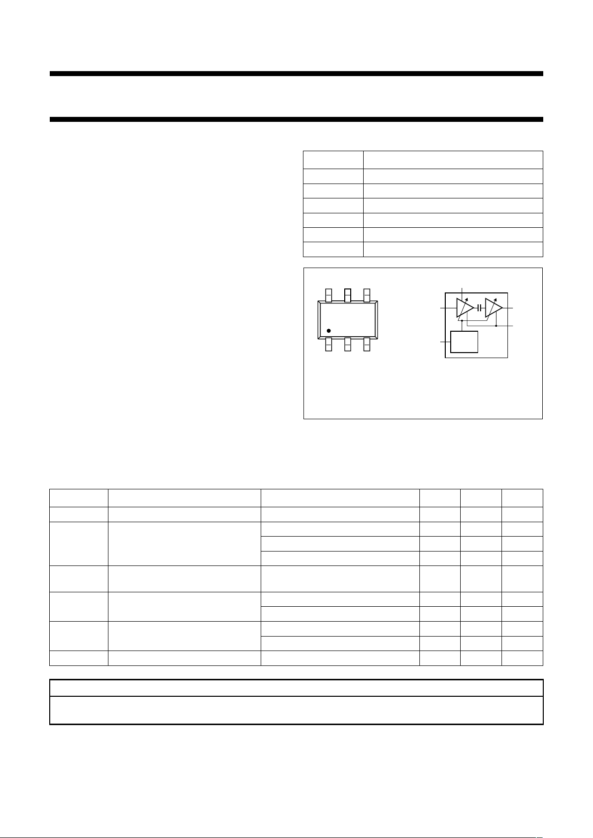
PIN DESCRIPTION
1RF in
2CTRL
3V
S1
4VS2+ RF out
5GND
6GND
Fig.1 Simplified outline (SOT363) and symbol.
Marking code: A3−
handbook, halfpage
MAM429
RFin
VS2+RFout
V
S1
CTRL
GND
Top view
BIAS
CIRCUIT
132
45
MSA370
123
654
Top view
QUICK REFERENCE DATA
SYMBOL PARAMETER CONDITIONS TYP. MAX. UNIT
V
S1
, V
S2
supply voltages 3 3.3 V
I
S
supply current into pin 3 + pin 4 V
CTRL
=0 0 10 µA
V
CTRL
= 2.7 V; VS=3V 51 63 mA
V
CTRL
= 2.4 V; VS=3V 30 37 mA
P
L
load power at 1 dB gain compression point;
f=1.9GHz
13 − dBm
ACPR adjacent channel power rejection f = 1.9 GHz; P
L
=10dBm 49 − dBc
f = 836 MHz; P
L
=8dBm 48 − dBc
G
p
power gain f = 1.9 GHz; PL=12dBm 23 − dB
f = 836 MHz; P
L
=8dBm 24 − dB
∆G gain control range f = 836 MHz; P
L
=8dBm 62 − dB
CAUTION
This product is supplied in anti-static packing to prevent damage caused by electrostatic discharge during transport
and handling. For further information, refer to Philips specs.: SNW-EQ-608, SNW-FQ-302A and SNW-FQ-302B.

2000 Feb 17 3
Philips Semiconductors Preliminary specification
MMIC variable gain amplifier BGA2031/1
LIMITING VALUES
In accordance with the Absolute Maximum Rating
System (IEC 134)
THERMAL RESISTANCE
SYMBOL PARAMETER CONDITIONS MIN. MAX. UNIT
V
S
DC supply voltage − 3.3 V
V
CTRL
control voltage − <V
S
V
I
CTRL
control current − 1.2 mA
I
S1
current into pin 3 − 27 mA
I
S2
current into pin 4 − 50 mA
P
D
drive power − tbf dBm
P
tot
total power dissipation Ts≤ 80 °C − 200 mW
T
stg
storage temperature −65 +150 °C
T
j
operating junction temperature − 150 °C
SYMBOL PARAMETER CONDITIONS VALUE UNIT
R
th j-s
thermal resistance from junction
to solder point
350 K/W
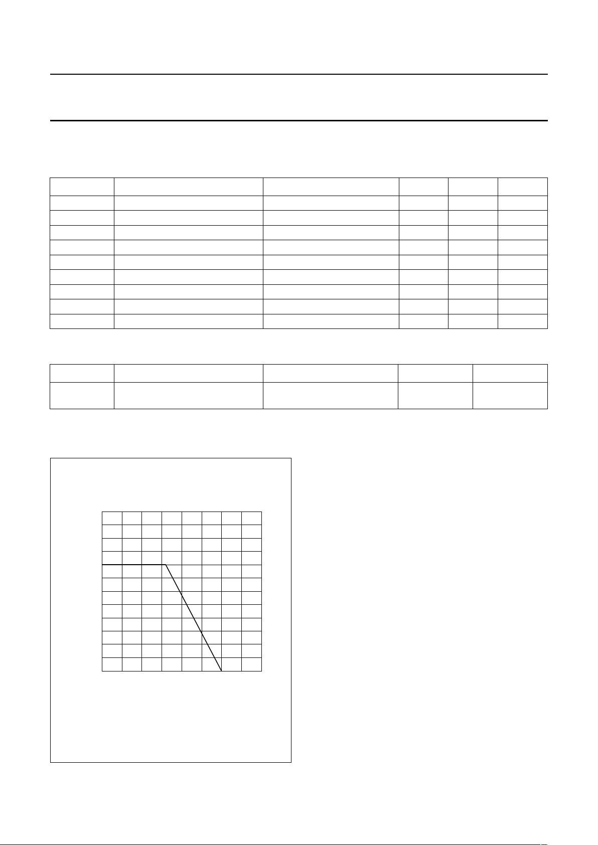
Fig.2 Power derating.
0
100
200
300
0 50 100 150 200
T
s
(°C)
P
tot
(mW)
 Loading...