

Philips BGA2031 Datasheet
DISCRETE SEMICONDUCTORS
DATA SH EET
M3D452
BGA2031
MMIC variable gain amplifier
Preliminary specification
Supersedes data of 1999 Feb 26
1999 Jul 23
Philips Semiconductors Preliminary specification
MMIC variable gain amplifier BGA2031
FEATURES
• High gain
• Excellent adjacent channel power rejection
• Small SMD package
• Low dissipation.
APPLICATIONS
• General purpose variable gain amplifier for low voltage
and medium power
• Driver for poweramplifiers in systems that require good
linearity, such as CDMA, both cellular band (850 MHz)
and PCS (1.9 GHz). This is because of the high output
power and good linearity.
DESCRIPTION
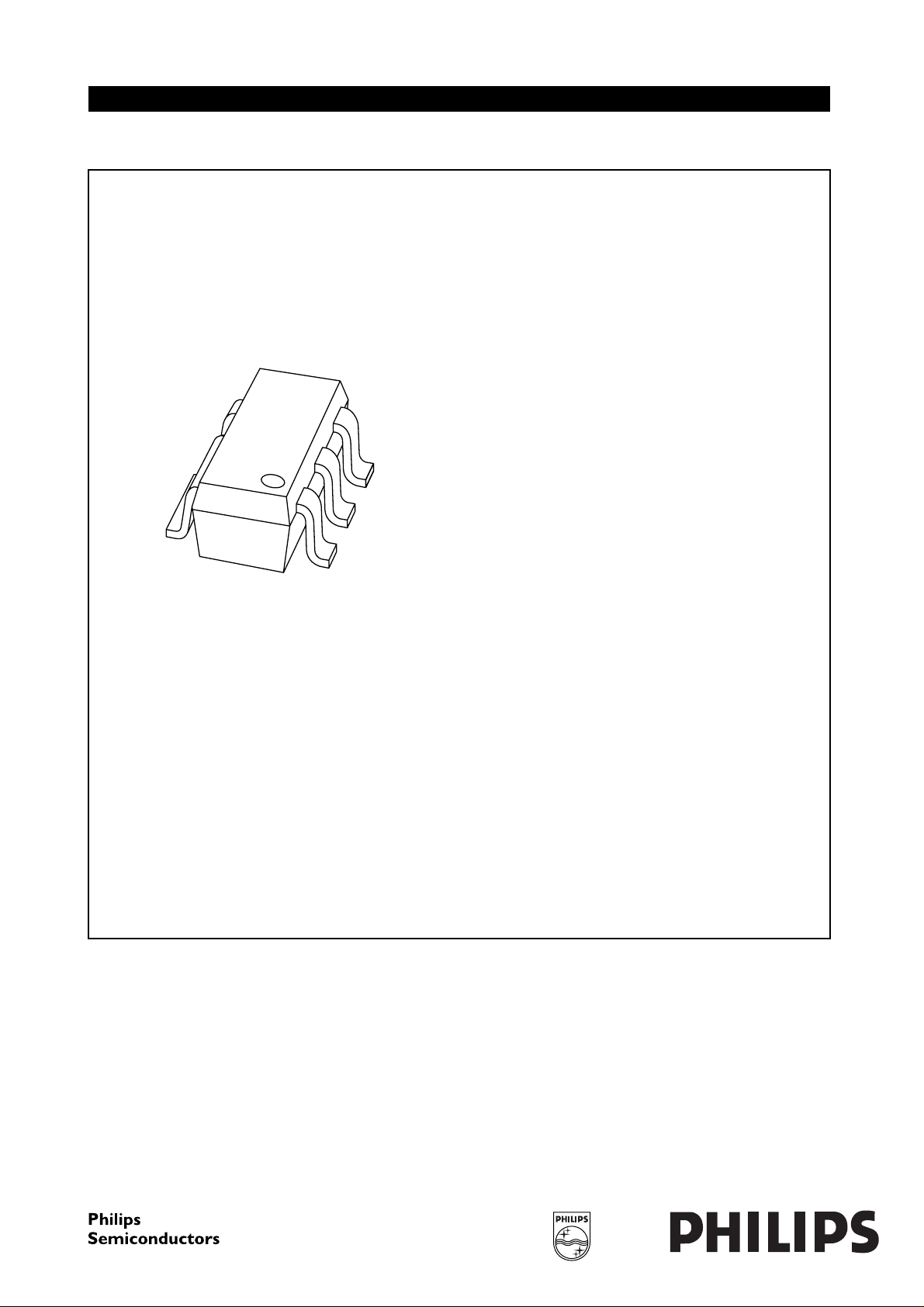
Silicon Monolitic Microwave Integrated Circuit (MMIC)
2 stage variable gain amplifier in double polysilicon
technology in a 5-pin SOT551A plastic SMD package for
low voltage medium power applications.
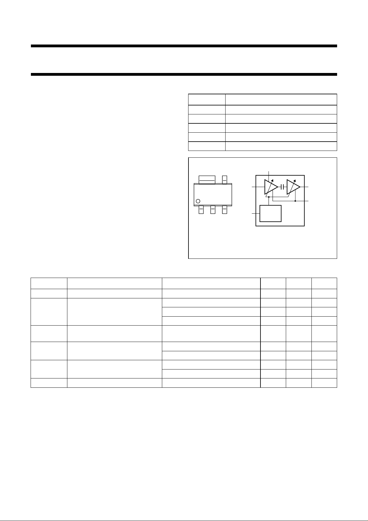
PINNING
PIN DESCRIPTION
1 RF in
2 CTRL
3V
S1
4VS2+ RF out
5 GND
handbook, halfpage
45
132
Top view
Marking code: G1.
RFin
CTRL
V
S1
BIAS
CIRCUIT
Fig.1 Simplified outline (SOT551A) and symbol.
VS2+RFout
GND
MAM429
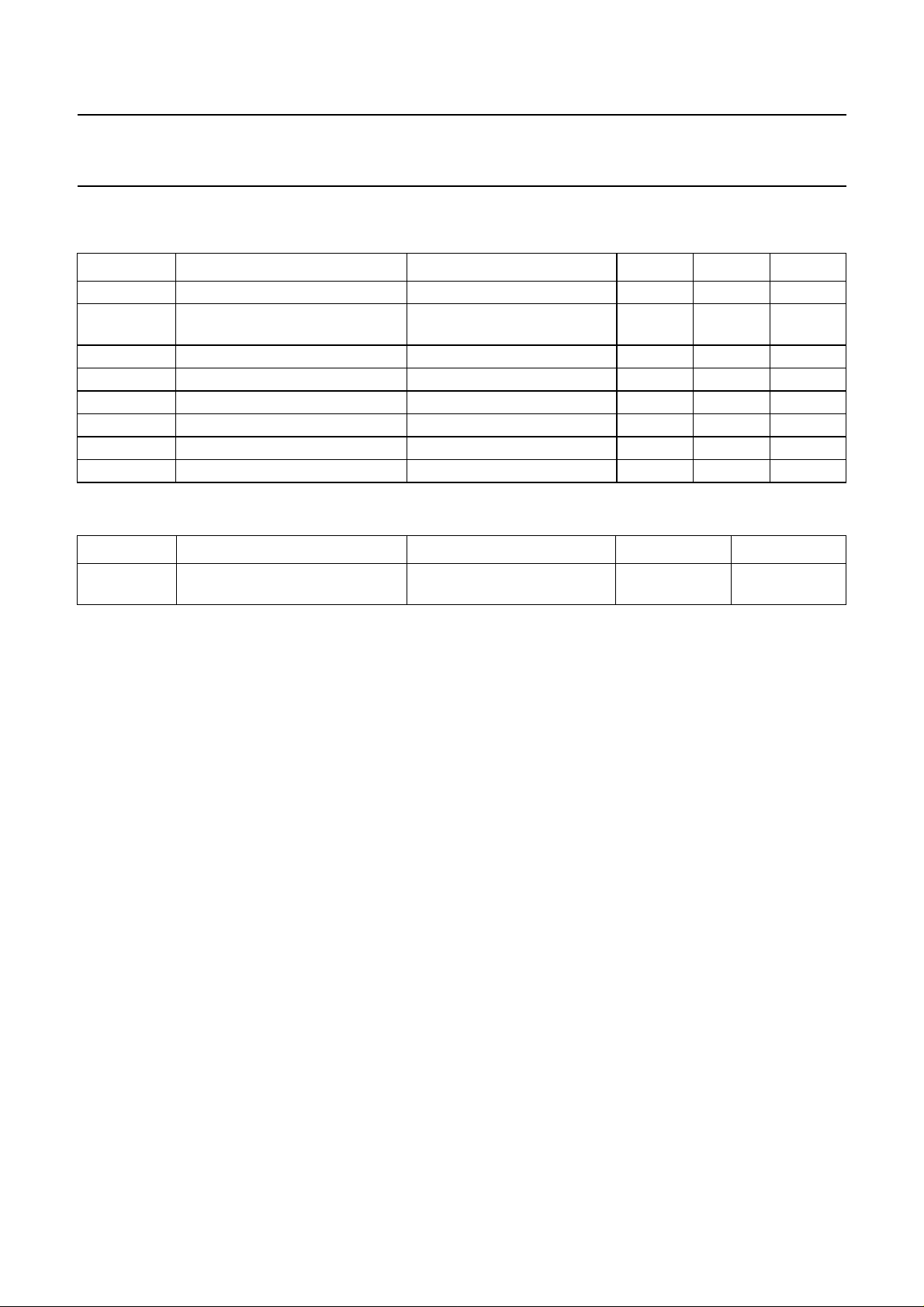
QUICK REFERENCE DATA
SYMBOL PARAMETER CONDITIONS TYP. MAX. UNIT
V
, V
S1
S2
I
S
P
L
supply voltages 3.6 4.1 V
supply current into pin 3 + pin 4 V
load power at 1 dB gain compression point;
=0 0 −µA
CTRL
V
= 2.7 V; VS=3.6V 5163mA
CTRL
V
= 2.4 V; VS=3V 3037mA
CTRL
13.5 − dBm
f = 1.9 GHz
ACPR adjacent channel power rejection f = 1.9 GHz; P
f = 836 MHz; P
G
p
power gain f = 1.9 GHz; PL= 12 dBm 26 − dB
f = 836 MHz; P
∆G gain control range f = 836 MHz; P
= 12 dBm 48 − dBc
L
= 8 dBm 55 − dBc
L
= 8 dBm 27 − dB
L
= 8 dBm 70 − dB
L
1999 Jul 23 2
Philips Semiconductors Preliminary specification
MMIC variable gain amplifier BGA2031
LIMITING VALUES
In accordance with the Absolute Maximum Rating System (IEC 134)
SYMBOL PARAMETER CONDITIONS MIN. MAX. UNIT
V
S
I
CTRL
I
S1
I
S2
P
D
P
tot
T
stg
T
j
THERMAL RESISTANCE
DC supply voltage − 4.2 V
control current V
CTRL
= 2.7 V;
− 1.2 mA
VS1= 4.2 V; VS2= 4.2 V
current into pin 3 VS1= 4.2 V − 27 mA
current into pin 4 VS2= 4.2 V − 50 mA
drive power − tbf dBm
total power dissipation Ts≤ 90 °C − 280 mW
storage temperature −65 +150 °C
operating junction temperature − 150 °C
SYMBOL PARAMETER CONDITIONS VALUE UNIT
R
th j-s
thermal resistance from junction
P
= 280 mW; Ts≤ 90 °C 215 K/W
tot
to solder point
1999 Jul 23 3
Philips Semiconductors Preliminary specification
MMIC variable gain amplifier BGA2031
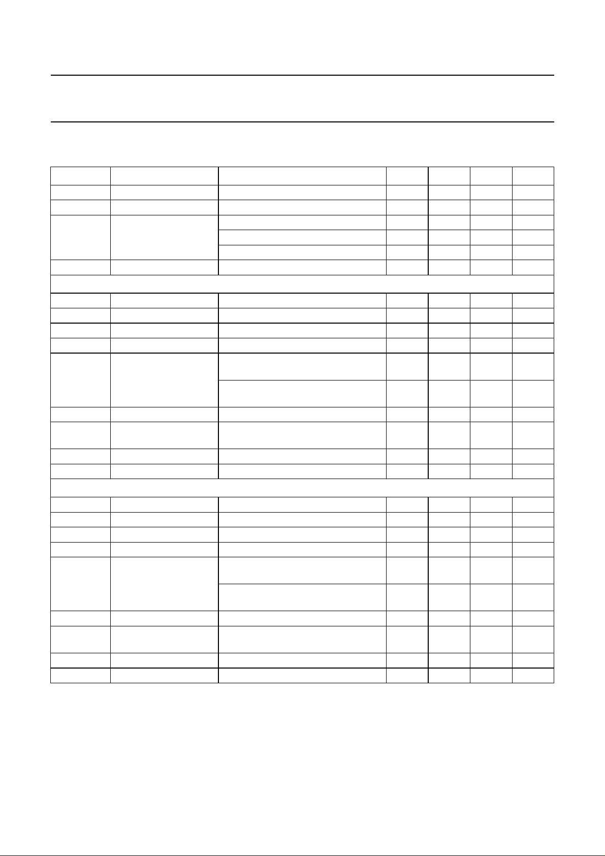
CHARACTERISTICS
Tj=25°C; ZS=ZL=50Ω; VS= 3.6 V; unless otherwise specified.
SYMBOL PARAMETER CONDITIONS MIN. TYP. MAX. UNIT
f frequency range 800 − 2500 MHz
, V
V
S1
S2
I
S
I
CTRL
f = 1900 MHz
f frequency range 1850 − 1950 MHz
G
P
∆G gain control range 0 < V
G
CS
ACPR adjacent channel power
P
L
P
N
VSWR
IN
VSWR
OUT
f = 836 MHz
f frequency range 824 − 849 MHz
G
P
∆G gain control range 0 < V
G
CS
ACPR adjacent channel power
P
L
P
N
VSWR
IN
VSWR
OUT
supply voltages 2.7 3.6 4.1 V
supply current
(in pin 3 + pin 4)
control current V
power gain V
V
=0 − 010µA
CTRL
= 2.7 V; VS=3.6V 395163mA
V
CTRL
V
= 2.4 V; VS=3V 233037mA
CTRL
= 2.7 V 0.7 0.92 1.1 mA
CTRL
= 2.7 V; PL= 12 dBm − 26 − dB
CTRL
< 2.7 V − 61 − dB
CTRL
gain control slope middle of ∆G − 38 − dB/V
rejection
±1.23 MHz offset; BW
BW
= 1.23 MHz; PL= 10 dBm
carrier
±1.98 MHz offset; BW
BW
= 1.23 MHz; PL= 10 dBm
carrier
ACP
ACP
= 30 kHz;
= 30 kHz;
− 48 − dBc
− 67 − dBc
load power at 1 dB gain compression point − 13.5 − dBm
noise power in CDMA receive band
− tbf − dBm/Hz
(1895 − 1955 MHz)
input VSWR V
output VSWR V
power gain V
= 2.7 V − 1:3.5 −
CTRL
= 2.7 V − 1:1.6 −
CTRL
= 2.7 V; PL= 8 dBm − 27 − dB
CTRL
< 2.7 V − 70 − dB
CTRL
gain control slope middle of ∆G − 40 − dB/V
rejection
±885 kHz offset; BW
BW
= 1.23 MHz; PL= 8 dBm
carrier
±1.98 MHz offset; BW
BW
= 1.23 MHz; PL= 8 dBm
carrier
ACP
ACP
= 30 kHz;
= 30 kHz;
− 55 − dBc
− 69 − dBc
load power at 1 dB gain compression point − 12 − dBm
noise power in CDMA receive band
− tbf − dBm/Hz
(869 to 894 MHz)
input VSWR V
output VSWR V
= 2.7 V − 1:2 −
CTRL
= 2.7 V − 1:1.7 −
CTRL
1999 Jul 23 4
 Loading...