


DISCRETE SEMICONDUCTORS
DATA SHEET
ook, halfpage
MBD128
BGA2022
MMIC mixer
Preliminary specification 2000 May 05
Philips Semiconductors Preliminary specification
MMIC mixer BGA2022
FEATURES
• Large frequency range:
– Cellular band (900 MHz)
– PCS band (1900 MHz)
– WLAN band (2.4 GHz).
• High isolation
• High linearity
• High conversion gain.
APPLICATIONS
Receiver side of wireless systems that require high
conversion gain and high linearity at low supply current,
such as CDMA.
DESCRIPTION
Silicon double poly MMIC mixer in a 6-lead plastic SOT363
package.
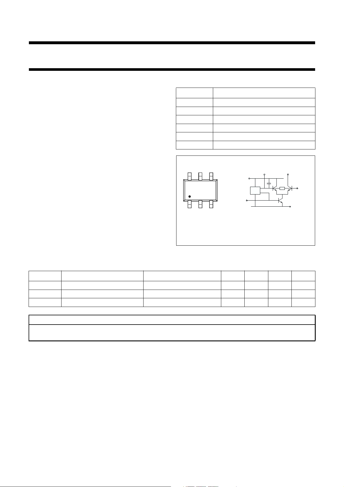
PINNING
PIN DESCRIPTION
1LO - GND
2 LO - signal
3V
S
4IF - out
5 RF - feedback
6 RF - signal
654
`
Bias
control
RF - signal (6)
123
Top view
MSA370
Fig.1 Simplified outline (SOT363) and symbol.
IF (4)LO - GND (1)
LO (2)
RF-feedback (5)
QUICK REFERENCE DATA
V
= 2.8V; IS=6mA; PLO=0dBm; fRF=1800MHz; fLO=2080MHz; fIF=280MHz.
S
SYMBOL PARAMETER CONDITIONS MIN. TYP. MAX. UNIT
G
conv
conversion gain 4 6 8 dB
NF noise figure (DSB) − 12 − dB
IP
3
output third order intercept point − 7 − dBm
CAUTION
This product is supplied in anti-static packing to prevent damage caused by electrostatic discharge during transport
and handling. For further information, refer to Philips specs.: SNW-EQ-608, SNW-FQ-302A and SNW-FQ-302B.
2000 May 05 2

Philips Semiconductors Preliminary specification
MMIC mixer BGA2022
LIMITING VALUES
In accordance with the Absolute Maximum Rating System (IEC 134).
SYMBOL PARAMETER CONDITIONS MIN. MAX. UNIT
V
S
I
S
P
LO
P
RF
P
tot
T
stg
T
j
Notes
1. LO and RF signals always AC coupled; 50 Ω source; no external DC voltage supplied to pin 1, 2 and 6.
2. T
is the temperature at the soldering point of the ground tab.
s
supply voltage − 4V
supply current − 10 mA
oscillator power note 1 − 10 dBm
RF power note 1 − 10 dBm
total power dissipation Ts≤ 100 °C; note 2 − 40 mW
storage temperature −65 +150 °C
junction temperature − 150 °C
THERMAL CHARACTERISTICS
SYMBOL PARAMETER VALUE UNIT
R
th j-s
thermal resistance from junction to solder point 375 K/W
CHARACTERISTICS
V
= 2.8 V; IS=6mA; Tj=25°C; see application report nr.: ; unless otherwise specified.
S
SYMBOL PARAMETER CONDITIONS MIN. TYP. MAX. UNIT
I
S
G
conv(p)
supply current VS=2.92V 468mA
power conversion gain PRF= −25 dBm; PLO=0dBm
880 MHz − 5 − dB
1800 MHz 468dB
1950 MHz − 5 − dB
2450 MHz − 6 − dB
NF noise figure DSB
880 MHz − 9 − dB
1800 MHz − 12 − dB
1950 MHz − 9 − dB
2450 MHz − 9 − dB
IP
3
intercept point third order input output refered
880 MHz − 4 − dBm
1800 MHz − 7 − dBm
1950 MHz − 7 − dBm
2450 MHz − 10 − dBm
VSWR
LO
return losses at LO port PLO=0dBm; f=0to3GHz −−2:1
2000 May 05 3
 Loading...