

Philips bga2011 DATASHEETS

DISCRETE SEMICONDUCTORS
DATA SHEET
ook, halfpage
MBD128
BGA2011
900 MHz high linear low noise
amplifier
Preliminary specification 2000 Aug 18
Philips Semiconductors Preliminary specification
900 MHz high linear low noise amplifier BGA2011
FEATURES
• Low current, low voltage
• High linearity
• High power gain
• Low noise
• Integrated temperature compensated biasing
• Control pin for adjustment bias current.
APPLICATIONS
• RF front end
• Low noise amplifiers, e.g. CDMA, PHs, Dect, etc.
DESCRIPTION
Silicon Monolitic Microwave Integrated Circuit (MMIC)
amplifier consisting of an NPN double polysilicon transistor
with integrated biasing for low voltage applications in a
6-pin SOT363 plastic SMD package.
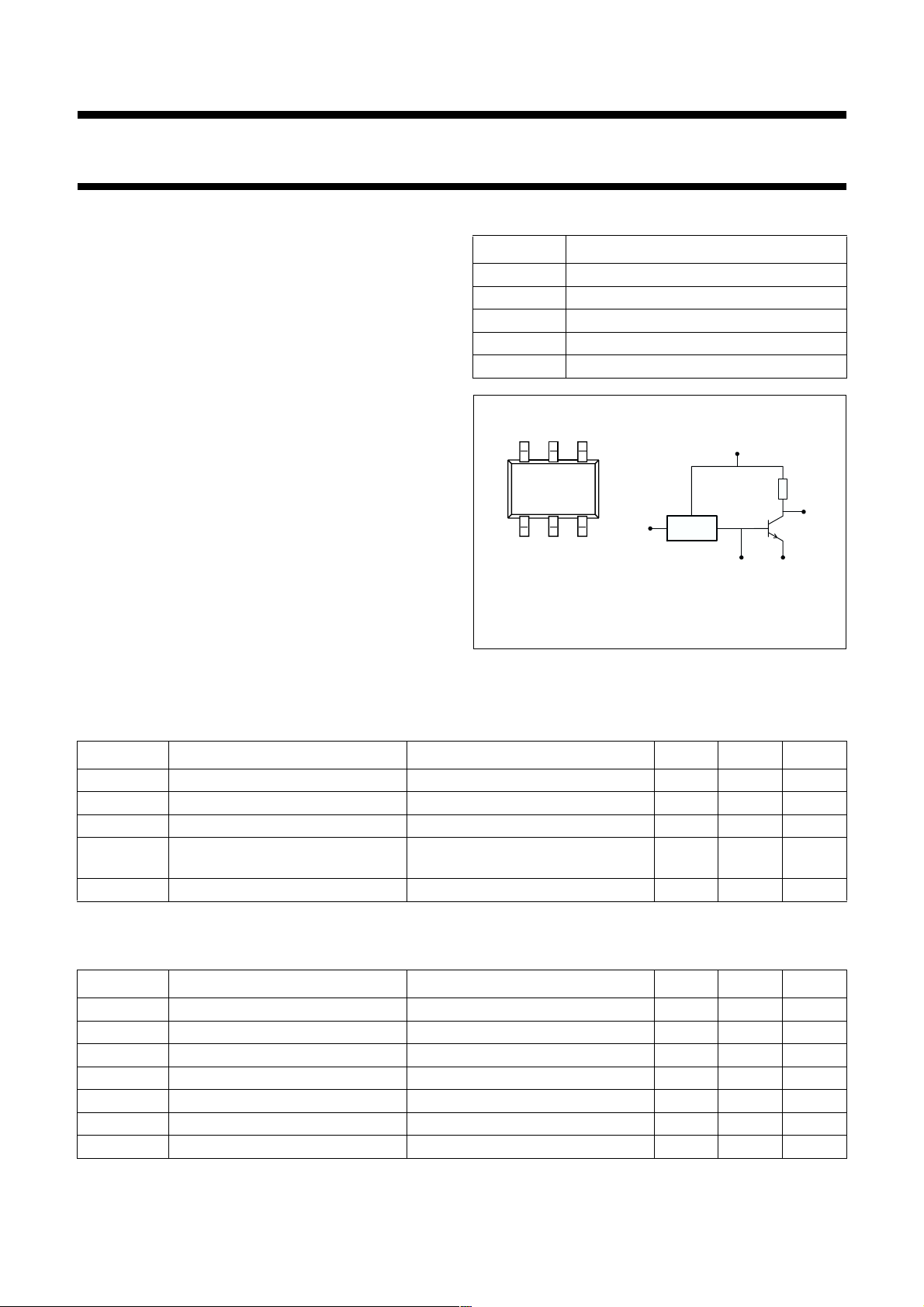
PINNING
PIN DESCRIPTION
1RF in
2V
3V
C
S
4 RF out
5, 6 GND
5
64
book, halfpage
1
Top view
Marking code:A5-
b
3
2
c
1
Bias
e
1
Circuit
b
2
MAM210
1
Vc
Fig.1 Simplified outline (SOT363) and symbol.
Vs
c
2
RF out
e
2
GNDRF in
QUICK REFERENCE DATA
SYMBOL PARAMETER CONDITIONS TYP. MAX. UNIT
V
I
I
|S
S
S
C
2
|
21
DC supply voltage RF input AC coupled 3 4.5 V
DC supply current 15 − mA
DC control current VC=V
S
insertion power gain in application circuit of Fig.2;
0.11 − mA
19 − dB
f = 900 MHz
NF noise figure I
=15mA; f=900MHz 1.7 − dB
S
LIMITING VALUES
In accordance with the Absolute Maximum Rating System (IEC 134)
SYMBOL PARAMETER CONDITIONS MIN. MAX. UNIT
V
S
V
C
I
S
I
C
P
tot
T
stg
T
j
DC supply voltage RF input AC coupled − 4.5 V
voltage on control pin − V
S
V
supply current forced by DC voltage on RF input − 30 mA
control current − 0.25 mA
total power dissipation Ts≤ 100 °C − 135 mW
storage temperature −65 +150 °C
operating junction temperature − 150 °C
2000 Aug 18 2
Philips Semiconductors Preliminary specification
900 MHz high linear low noise amplifier BGA2011
THERMAL RESISTANCE
SYMBOL PARAMETER CONDITIONS VALUE UNIT
R
th j-s
CHARACTERISTICS
RF input AC coupled; V
SYMBOL PARAMETER CONDITIONS MIN. TYP. MAX. UNIT
I
S
I
C
R
L IN
R
L OUT
2
|S
|
21
NF noise figure typical application (see Fig.2);
IP3
(in)
thermal resistance from junction
P
= 135 mW; Ts≤ 100 °C 350 K/W
tot
to solder point
=3V; IS= 15 mA; f = 900 MHz; Tj=25°C; unless otherwise specified.
S
supply current 10 15 20 mA
control current − 0.11 − mA
return losses input typical application (see Fig.2) −−11 − dB
high IP3 (see Fig.2; stripline = 0 mm) −−11 − dB
high IP3 (see Fig.2; stripline = 1.5 mm) −−17 − dB
return losses output typical application (see Fig.2) −−11 − dB
high IP3 (see Fig.2; stripline = 0 mm) −−12 − dB
high IP3 (see Fig.2; stripline = 1.5 mm) −−14 − dB
insertion power gain typical application (see Fig.2) − 15 − dB
high IP3 (see Fig.2; stripline = 0 mm) − 19 − dB
high IP3 (see Fig.2; stripline = 1.5 mm) − 16 − dB
− 1.5 − dB
I
=15mA
S
high IP3 (see Fig.2; stripline = 0 mm) − 1.6 − dB
high IP3 (see Fig.2; stripline = 1.5 mm) − 1.7 − dB
input intercept point typical application (see Fig.2) −−2 − dBm
high IP3 (see Fig.2; stripline = 0 mm) − 4 − dBm
high IP3 (see Fig.2; stripline = 1.5 mm) − 10 − dBm
2000 Aug 18 3
Philips Semiconductors Preliminary specification
900 MHz high linear low noise amplifier BGA2011
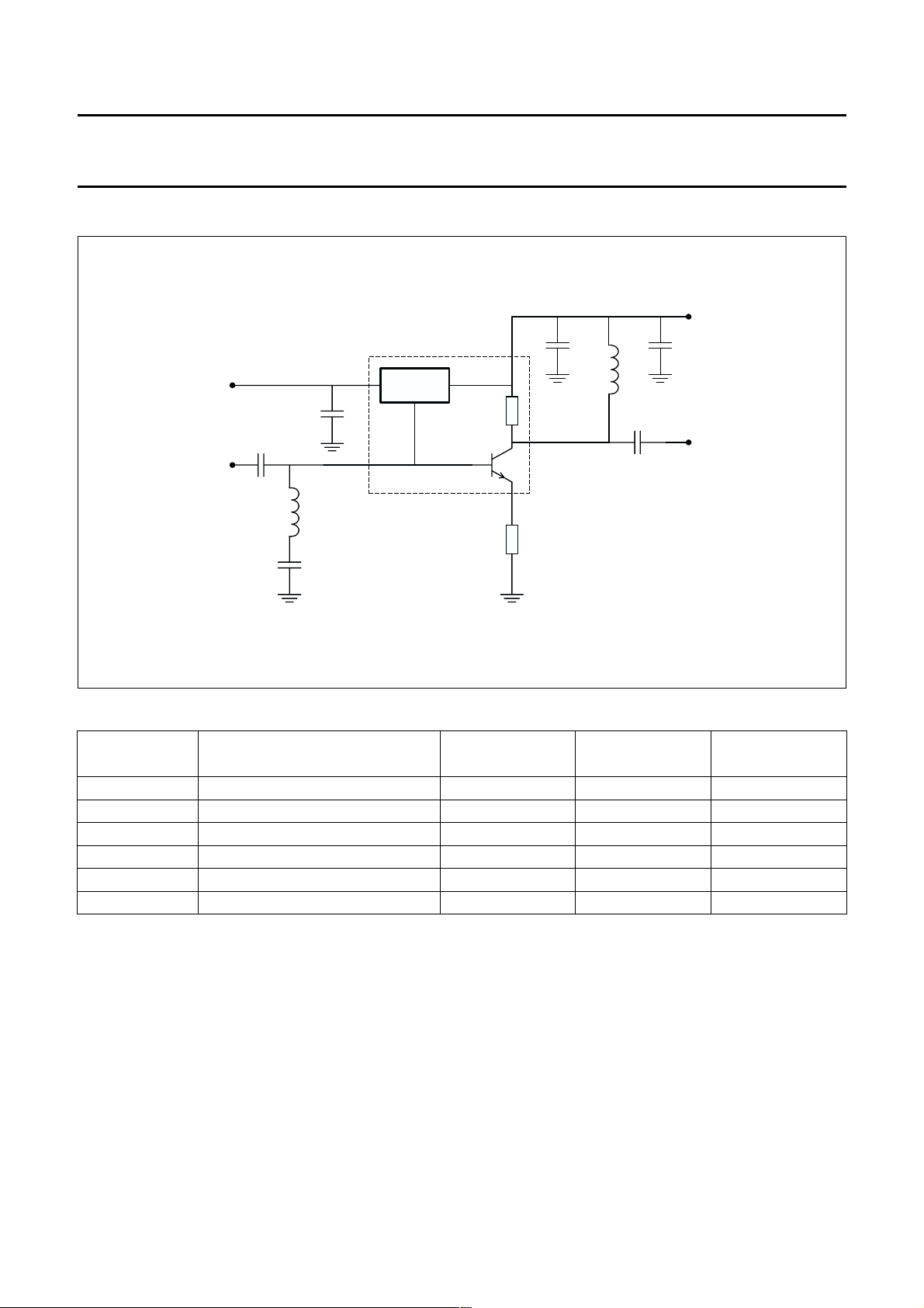
ELECTRICAL BLOCK DIAGRAM
Vs
Vc
RF in
C
Out
4
L
2
Vs
Vc
C
C
1
5
In
L
1
C
6
Bias
Circuit
SOT363
GND
stripline
C
3
C
2
RF out
Fig.2 Application circuit
List of components (see Fig.2)
COMPONENT DESCRIPTION
TYPICAL
APPLICATION
HIGH IP3
APPLICATION
DIMENSIONS
C1, C2 multilayer ceramic chip capacitor 100 pF 100 pF 0603
C3, C5 multilayer ceramic chip capacitor 22 nF 22 nF 0603
C4 multilayer ceramic chip capacitor 5.6 pF 5.6 pF 0603
C6 multilayer ceramic chip capacitor − 2 x 100 nF 0805
L1 SMD inductor − 10 nH 0603
L2 SMD inductor − 8.2 nH 0603
Note
1. The stripline is on a gold plated double copper-clad printed-circuit board (ε
= 6.15), board thickness = 0.64 mm,
r
copper thickness = 35 µm, gold thickness = 5 µm.
2000 Aug 18 4
 Loading...