


DISCRETE SEMICONDUCTORS
DATA SH EET
BFT93
PNP 5 GHz wideband transistor
Product specification
File under Discrete Semiconductors, SC14
November 1992
Philips Semiconductors Product specification
PNP 5 GHz wideband transistor BFT93
DESCRIPTION
PNP transistor in a plastic SOT23
envelope.
It is primarily intended for use in RF
wideband amplifiers, such as in aerial
amplifiers, radar systems,
oscilloscopes, spectrum analyzers,
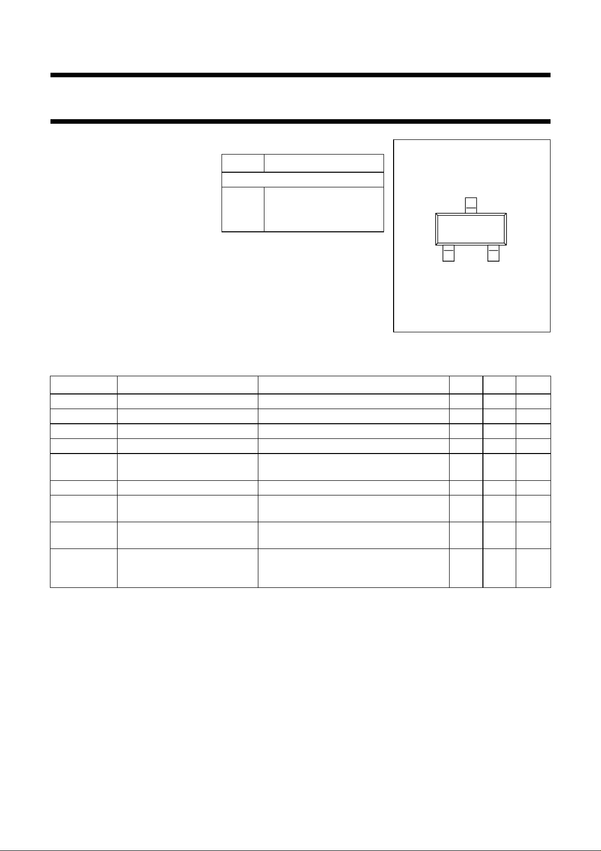
PINNING
PIN DESCRIPTION
Code: X1p
1 base
2 emitter
3 collector
page
3
etc. The transistor features low
intermodulation distortion and high
power gain; due to its very high
transition frequency, it also has
12
Top view
MSB003
excellent wideband properties and
low noise up to high frequencies.
NPN complements are BFR93 and
Fig.1 SOT23.
BFR93A.
QUICK REFERENCE DATA
SYMBOL PARAMETER CONDITIONS TYP. MAX. UNIT
V
V
I
P
f
CBO
CEO
c
tot
T
collector-base voltage open emitter −−15 V
collector-emitter voltage open base −−12 V
DC collector current −−35 mA
total power dissipation up to Ts=95°C; note 1 − 300 mW
transition frequency IC= −30 mA; VCE= −5 V; f = 500 MHz;
5 − GHz
Tj=25°C
C
re
G
UM
F noise figure I
V
o
feedback capacitance IC= −2 mA; VCE= −5 V; f = 1 MHz 1 − pF
maximum unilateral power gain IC= −30 mA; VCE= −5 V; f = 500 MHz;
T
=25°C
amb
= −10 mA; VCE= −5 V; f = 500 MHz;
C
T
=25°C
amb
output voltage dim= −60 dB; IC= −30 mA;
16.5 − dB
2.4 − dB
300 − mV
VCE= −5 V; RL=75Ω;
f
= 493.25 MHz
(p+q−r)
Note
1. T
is the temperature at the soldering point of the collector tab.
s
November 1992 2

Philips Semiconductors Product specification
PNP 5 GHz wideband transistor BFT93
LIMITING VALUES
In accordance with the Absolute Maximum System (IEC 134).
SYMBOL PARAMETER CONDITIONS MIN. MAX. UNIT
V
CBO
V
CEO
V
EBO
I
C
I
CM
P
tot
T
stg
T
j
THERMAL RESISTANCE
SYMBOL PARAMETER CONDITIONS THERMAL RESISTANCE
R
th j-s
collector-base voltage open emitter −−15 V
collector-emitter voltage open base −−12 V
emitter-base voltage open collector −−2V
DC collector current −−35 mA
peak collector current f > 1 MHz −−50 mA
total power dissipation up to Ts=95°C; note 1 − 300 mW
storage temperature −65 150 °C
junction temperature − 175 °C
thermal resistance from junction to
up to Ts=70°C; (note 1) 260 K/W
soldering point
Note
1. T
is the temperature at the soldering point of the collector tab.
s
November 1992 3
 Loading...