

Philips BFS17A Datasheet

DISCRETE SEMICONDUCTORS
DATA SH EET
BFS17A
NPN 3 GHz wideband transistor
Product specification
File under Discrete Semiconductors, SC14
September1995
Philips Semiconductors Product specification
NPN 3 GHz wideband transistor BFS17A
DESCRIPTION
NPN transistor in a plastic SOT23 package.
APPLICATIONS
• It is intended for RF applications such as oscillators
in TV tuners.
PINNING
PIN DESCRIPTION
1 base
2 emitter
3 collector
QUICK REFERENCE DATA
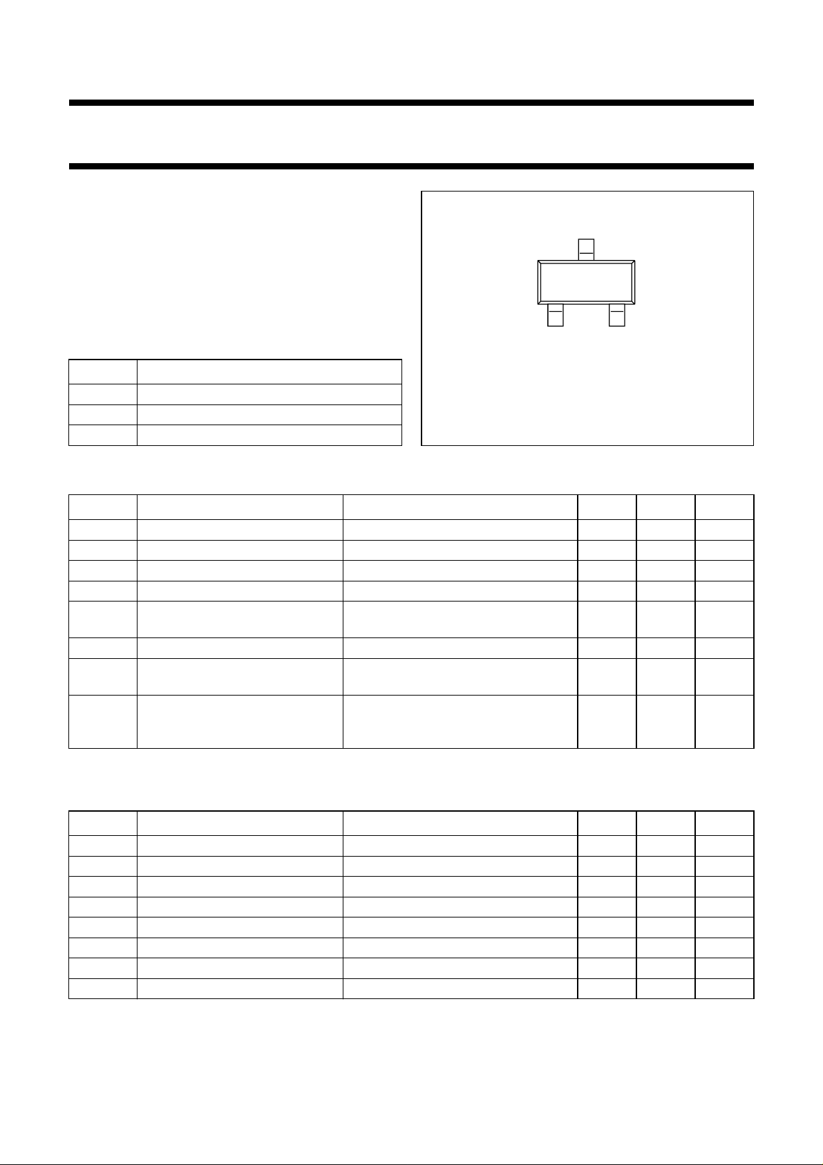
handbook, halfpage
12
Top view
Marking code: E2p.
Fig.1 SOT23.
3
MSB003
SYMBOL PARAMETER CONDITIONS TYP. MAX. UNIT
V
CBO
V
CEO
I
C
P
tot
f
T
G
UM
F noise figure I
V
O
collector-base voltage open emitter − 25 V
collector-emitter voltage open base − 15 V
DC collector current − 25 mA
total power dissipation up to Ts=70°C; note 1 − 300 mW
transition frequency IC= 25 mA; VCE= 5 V; f = 500 MHz;
T
=25°C
amb
2.8 − GHz
maximum unilateral power gain IC= 14 mA; VCE= 10 V; f = 800 MHz 13.5 − dB
= 2 mA; VCE= 5 V; f = 800 MHz;
C
T
=25°C
amb
output voltage dim= −60 dB; IC= 14 mA; VCE=10V;
RL=75Ω; T
f
= 793.25 MHz
(p+q−r)
amb
=25°C;
2.5 − dB
150 − mV
LIMITING VALUES
In accordance with the Absolute Maximum Rating System (IEC 134).
SYMBOL PARAMETER CONDITIONS MIN. MAX. UNIT
V
V
V
I
I
P
T
T
CBO
CEO
EBO
C
CM
tot
stg
j
collector-base voltage open emitter − 25 V
collector-emitter voltage open base − 15 V
emitter-base voltage open collector − 2.5 V
DC collector current − 25 mA
peak collector current − 50 mA
total power dissipation up to Ts=70°C; note 1 − 300 mW
storage temperature −65 +150 °C
junction temperature − 150 °C
Note to the Quick reference data and the Limiting values
is the temperature at the soldering point of the collector pin.
1. T
s
September1995 2
 Loading...