

Philips BFR94A Datasheet

DISCRETE SEMICONDUCTORS
DATA SH EET
BFR94A
NPN 3.5 GHz wideband transistor
Product specification
File under Discrete Semiconductors, SC14
September 1995
Philips Semiconductors Product specification
NPN 3.5 GHz wideband transistor BFR94A
DESCRIPTION
NPN resistance-stabilized transistor
in a SOT122E capstan envelope.
It features extremely low cross
modulation, intermodulation and
second order intermodulation
distortion. Due to its high transition
frequency, it has a high power gain, in
conjunction with good wideband
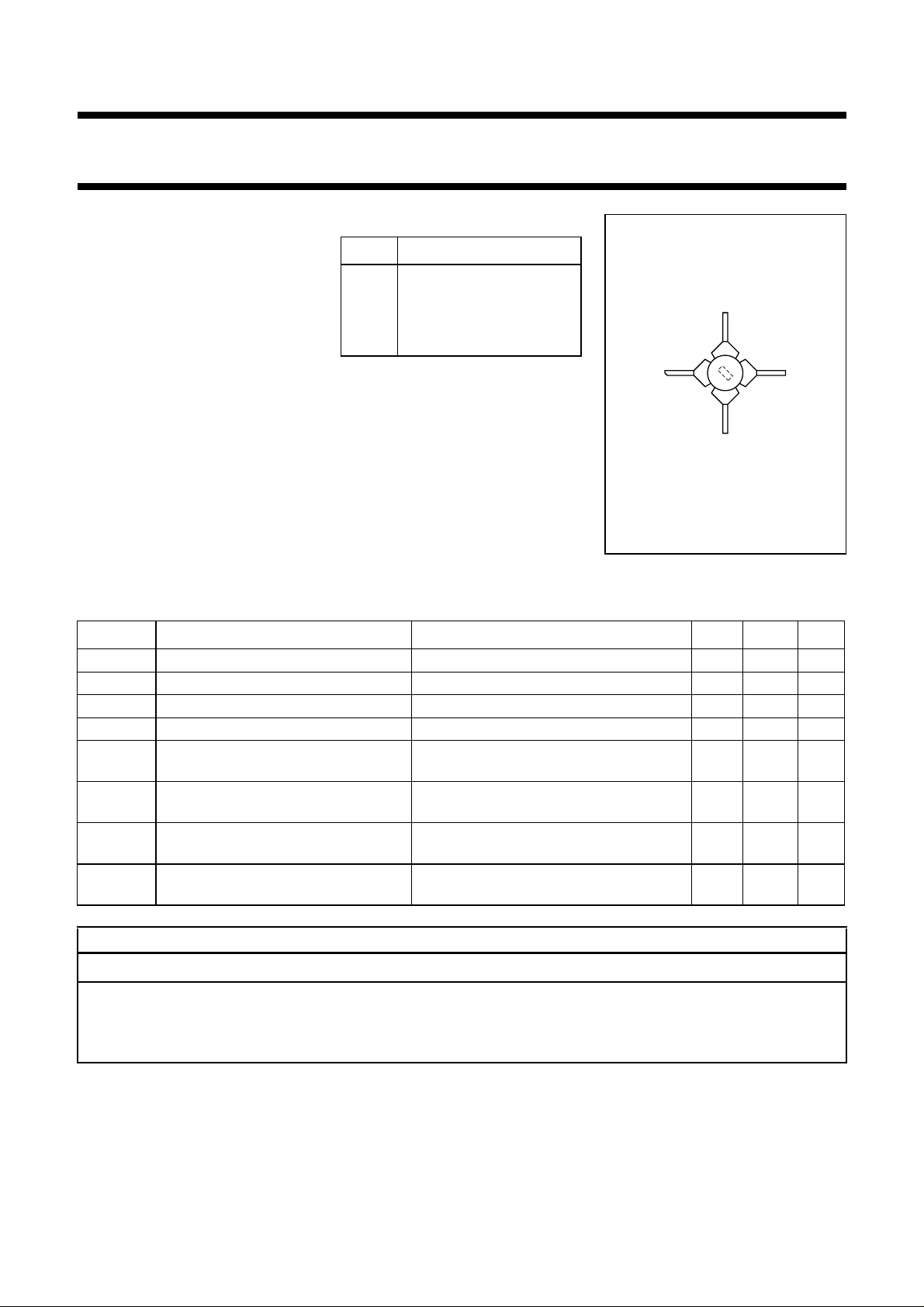
PINNING
PIN DESCRIPTION
1 collector
2 emitter
3 base
4 emitter
fpage
4
C
1
3
properties, and low noise up to high
frequencies.
2
MBB904
It is primarily intended for CATV and
MATV applications.
The BFR94A is a replacement for the
BFR94. The SOT122E footprint is
similar to that of the SOT48, used for
Fig.1 SOT122E.
the BFR94.
QUICK REFERENCE DATA
SYMBOL PARAMETER CONDITIONS TYP. MAX. UNIT
V
V
I
P
f
CBO
CEO
C
tot
T
collector-base voltage open emitter − 30 V
collector-emitter voltage open base − 25 V
DC collector current − 150 mA
total power dissipation up to Tc= 145 °C; f > 1 MHz − 3.5 W
transition frequency Ic= 90 mA; VCE= 20 V; f = 500 MHz;
3.5 − GHz
Tj=25°C
F noise figure I
d
im
d
2
intermodulation distortion Ic= 90 mA; VCE= 20 V;
second order intermodulation
distortion
= 90 mA; VCE= 20 V; f = 200 MHz;
c
=25°C
T
amb
Vo= 60 dBmV; f
= 194.25 MHz
(p+q−r)
Ic= 90 mA; VCE= 20 V;
Vo= 48 dBmV; fp+ fq= 210 MHz
810dB
−63 − dB
−−56 dB
WARNING
Product and environmental safety - toxic materials
This product contains beryllium oxide. The product is entirely safe provided that the BeO disc is not damaged. All
persons who handle, use or dispose of this product should be aware of its nature and of the necessary safety
precautions. After use, dispose of as chemical or special waste according to the regulations applying at the location of
the user. It must never be thrown out with the general or domestic waste.
September 1995 2

Philips Semiconductors Product specification
NPN 3.5 GHz wideband transistor BFR94A
LIMITING VALUES
In accordance with the Absolute Maximum System (IEC 134).
SYMBOL PARAMETER CONDITIONS MIN. MAX. UNIT
V
CBO
V
CEO
V
CER
V
EBO
I
C
I
CM
P
tot
T
stg
T
j
THERMAL RESISTANCE
collector-base voltage open emitter − 30 V
collector-emitter voltage open base − 25 V
collector-emitter voltage RBE= 100 Ω−35 V
emitter-base voltage open collector − 3V
DC collector current − 150 mA
peak collector current f > 1 MHz − 300 mA
total power dissipation up to Tc= 145 °C; f > 1 MHz − 3.5 W
storage temperature −65 200 °C
junction temperature − 200 °C
SYMBOL PARAMETER THERMAL RESISTANCE
R
th j-c
thermal resistance from junction to case 15 K/W
September 1995 3
 Loading...