

Philips BFR93A Datasheet

DISCRETE SEMICONDUCTORS
DATA SH EET
BFR93A
NPN 6 GHz wideband transistor
Product specification
Supersedes data of September 1995
File under discrete semiconductors, SC14
1997 Oct 29
Philips Semiconductors Product specification
NPN 6 GHz wideband transistor BFR93A
FEATURES
• High power gain
• Low noise figure
• Very low intermodulation distortion.
APPLICA TIONS
• RF wideband amplifiers and
oscillators.
DESCRIPTION
NPN wideband transistor in a plastic
SOT23 package.
PNP complement: BFT93.
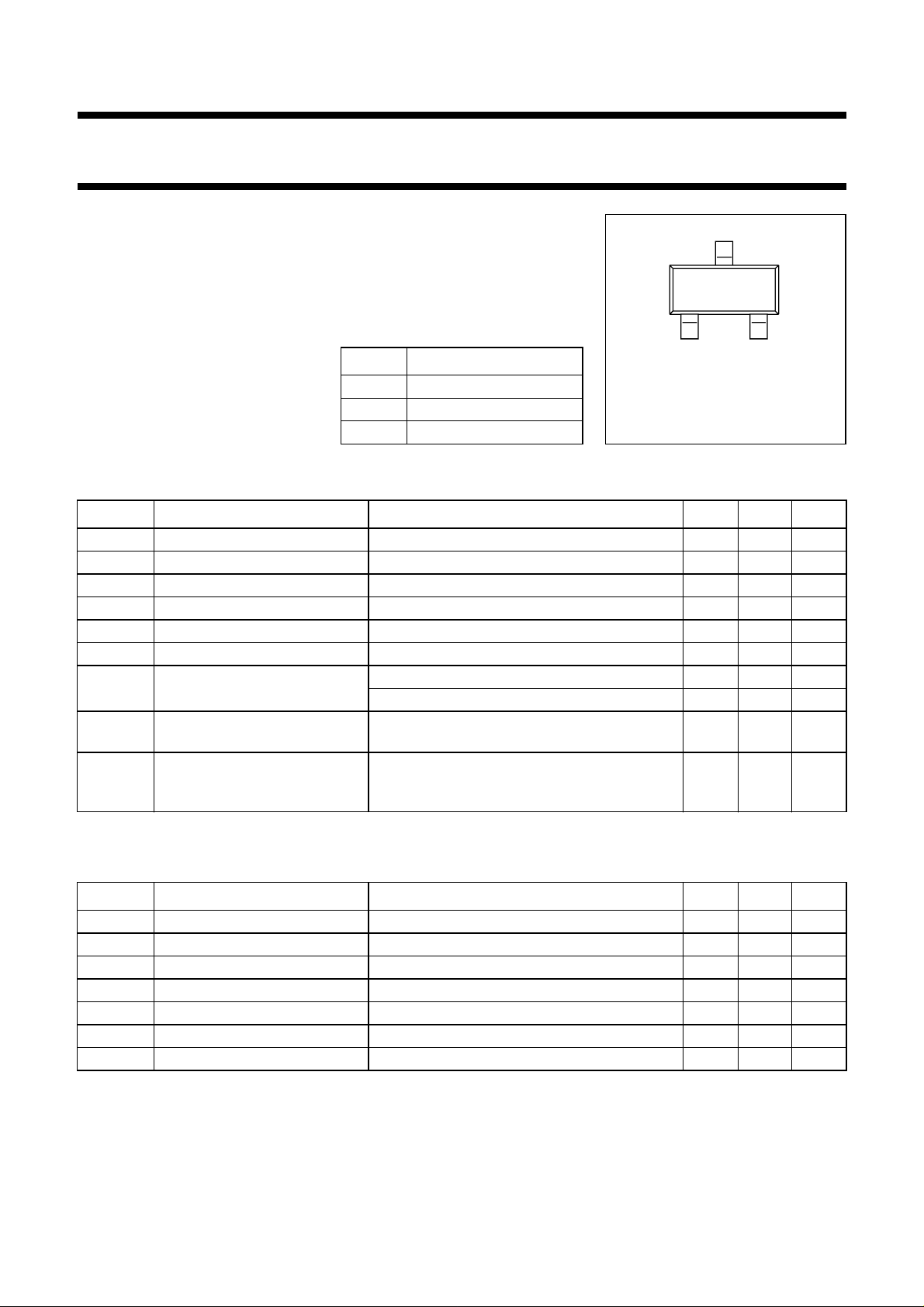
PINNING
PIN DESCRIPTION
1 base
2 emitter
page
Marking code: R2p.
3
12
Top view
MSB003
Fig.1 SOT23.
3 collector
QUICK REFERENCE DATA
SYMBOL PARAMETER CONDITIONS TYP. MAX. UNIT
V
CBO
V
CEO
I
C
P
tot
C
re
f
T
G
UM
F noise figure I
V
O
collector-base voltage open emitter − 15 V
collector-emitter voltage open base − 12 V
collector current (DC) − 35 mA
total power dissipation Ts≤ 95 °C − 300 mW
feedback capacitance IC= 0; VCE= 5 V; f = 1 MHz 0.6 − pF
transition frequency IC= 30 mA; VCE= 5 V; f = 500 MHz 6 − GHz
maximum unilateral power gain IC= 30 mA; VCE= 8 V; f = 1 GHz; T
I
= 30 mA; VCE= 8 V; f = 2 GHz; T
C
= 5 mA; VCE= 8 V; f = 1 GHz; Γs= Γ
C
T
=25°C
amb
output voltage dim= −60 dB; IC= 30 mA; VCE=8V;
RL=75Ω; T
amb
=25°C;
=25°C13 − dB
amb
=25°C7 − dB
amb
opt
;
1.9 − dB
425 − mV
fp+fq−fr= 793.25 MHz
LIMITING VALUES
In accordance with the Absolute Maximum Rating System (IEC 134).
SYMBOL PARAMETER CONDITIONS MIN. MAX. UNIT
V
CBO
V
CEO
V
EBO
I
C
P
tot
T
stg
T
j
collector-base voltage open emitter − 15 V
collector-emitter voltage open base − 12 V
emitter-base voltage open collector − 2V
collector current (DC) − 35 mA
total power dissipation Ts≤ 95 °C; note 1 − 300 mW
storage temperature −65 +150 °C
junction temperature − +175 °C
Note
1. T
is the temperature at the soldering point of the collector pin.
s
1997 Oct 29 2

Philips Semiconductors Product specification
NPN 6 GHz wideband transistor BFR93A
THERMAL CHARACTERISTICS
SYMBOL PARAMETER CONDITIONS VALUE UNIT
R
th j-s
Note
1. T
s
CHARACTERISTICS
=25°C unless otherwise specified.
T
j
SYMBOL PARAMETER CONDITIONS MIN. TYP. MAX. UNIT
I
CBO
h
FE
C
c
C
e
C
re
f
T
G
UM
F noise figure (note 2) I
V
O
d
2
thermal resistance from junction to soldering point Ts≤ 95 °C; note 1 260 K/W
is the temperature at the soldering point of the collector pin.
collector cut-off current IE= 0; VCB=5V −−50 nA
DC current gain IC= 30 mA; VCE= 5 V 40 90 −
collector capacitance IE=ie= 0; VCB=5V; f=1MHz − 0.7 − pF
emitter capacitance IC=ic= 0; VEB= 0.5 V; f = 1 MHz − 1.9 − pF
feedback capacitance IC=ic= 0; VCE= 5 V; f = 1 MHz;
T
=25°C
amb
− 0.6 − pF
transition frequency IC= 30 mA; VCE= 5 V; f = 500 MHz 4.5 6 − GHz
maximum unilateral power gain
(note 1)
IC= 30 mA; VCE= 8 V; f = 1 GHz;
T
=25°C
amb
= 30 mA; VCE= 8 V; f = 2 GHz;
I
C
T
=25°C
amb
= 5 mA; VCE= 8 V; f = 1 GHz;
C
Γs= Γ
I
C
Γs= Γ
; T
amb
=25°C
opt
= 5 mA; VCE= 8 V; f = 2 GHz;
; T
amb
=25°C
opt
− 13 − dB
− 7 − dB
− 1.9 − dB
− 3 − dB
output voltage notes 2 and 3 − 425 − mV
second order intermodulation
notes 2 and 4 −−50 − dB
distortion
Notes
1. G
is the maximum unilateral power gain, assuming S12 is zero and .
UM
2. Measured on the same die in a SOT37 package (BFR91A).
3. d
= −60 dB (DIN 45004B); IC= 30 mA; VCE= 8 V; RL=75Ω; T
im
Vp=VOat dim= −60 dB; fp= 795.25 MHz;
Vq=VO−6 dB at fq= 803.25 MHz;
Vr=VO−6 dB at fr= 805.25 MHz;
measured at fp+fq−fr= 793.25 MHz.
4. IC= 30 mA; VCE= 8 V; RL=75Ω; T
amb
=25°C;
Vp= 200 mV at fp= 250 MHz;
Vq= 200 mV at fq= 560 MHz;
measured at fp+fq= 810 MHz.
1997 Oct 29 3
amb
G
UM
=25°C;
10 log
--------------------------------------------------------------
1
S
–
11
2
S
21
2
1
–
dB=
2
S
22

Philips Semiconductors Product specification
NPN 6 GHz wideband transistor BFR93A
handbook, full pagewidth
L1=L3=5µH choke.
L2 =3 turns 0.4 mm copper wire; winding pitch 1 mm; internal diameter 3 mm.
V
BB
75 Ω
input
1.5 nF
1 nF
10 kΩ
L1
L2
270 Ω
3.3 pF
Fig.2 Intermodulation distortion and second harmonic distortion MATV test circuit.
1 nF
1.5 nF
L3
DUT
18 Ω
1 nF
0.68 pF
MBB251
V
CC
75 Ω
output
150
Ts(
MBG246
o
C)
400
handbook, halfpage
P
tot
(mW)
300
200
100
0
0 50 100 200
Fig.3 Power derating curve.
1997 Oct 29 4
120
handbook, halfpage
h
FE
80
40
0
0102030
VCE= 5 V; Tj=25°C.
Fig.4 DC current gain as a function of
collector current.
I (mA)
C
MCD087
 Loading...