

Page 1

BFR505
NPN 9 GHz wideband transistor
Rev. 03 — 20 July 2004 Product data sheet
1. Product profile
1.1 General description
The BFR505 is an NPN silicon planar epitaxial transistor, intended for applications in the
RF front end in wideband applications in the GHz range, such as analog and digital
cellular telephones, cordless telephones (CT1, CT2, DECT, etc.), radar detectors, pagers
and satellite TV tuners (SATV).
The transistor is encapsulated in a plastic SOT23 envelope.
1.2 Features
■ High power gain
■ Low noise figure
■ High transition frequency
■ Gold metallization ensures excellent reliability.
1.3 Quick reference data
Table 1: Quick reference data
Symbol Parameter Conditions Min Typ Max Unit
V
V
I
P
h
C
f
G
S
C
FE
T
CBO
CES
tot
re
UM
21
collector-base
voltage
collector-emitter
voltage
DC collector
current
total power
dissipation
DC current gain IC = 5 mA; VCE = 6 V 60 120 250
feedback
capacitance
transition frequency IC = 5 mA; VCE = 6 V; f = 1 GHz - 9 - GHz
maximum unilateral
power gain
2
insertion power
gain
open emitter - - 20 V
RBE = 0 Ω --15V
--18mA
up to Ts = 135 °C
IC = ic = 0 A; VCB = 6 V; f = 1 MHz - 0.3 - pF
IC = 5 mA; VCE = 6 V;
T
= 25 °C; f = 900 MHz
amb
= 5 mA; VCE = 6 V;
I
C
T
= 25 °C; f = 2 GHz
amb
IC = 5 mA; VCE = 6 V;
T
= 25 °C; f = 900 MHz
amb
[1]
- - 150 mW
-17-dB
-10-dB
13 14 - dB
Page 2

Philips Semiconductors
BFR505
NPN 9 GHz wideband transistor
Table 1: Quick reference data
Symbol Parameter Conditions Min Typ Max Unit
F noise figure Γs = Γ
[1] Ts is the temperature at the soldering point of the collector tab.
2. Pinning information
Table 2: Discrete pinning
Pin Description Simplified outline Symbol
1 base
2 emitter
3 collector
…continued
; IC = 1.25 mA; VCE = 6 V;
opt
T
= 25 °C; f = 900 MHz
amb
= Γ
Γ
T
Γ
T
; IC = 5 mA; VCE = 6 V;
s
opt
= 25 °C; f = 900 MHz
amb
= Γ
; IC = 1.25 mA; VCE = 6 V;
s
opt
= 25 °C; f = 2 GHz
amb
- 1.2 1.7 dB
- 1.6 2.1 dB
- 1.9 - dB
3
1
12
SOT23
sym021
3
2
3. Ordering information
Table 3: Ordering information
Type number Package
BFR505 - plastic surface mounted package; 3 leads SOT23
4. Marking
Table 4: Marking table
Type number Marking code
BFR505 31*
[1] * = p: made in Hong Kong.
* = t: made in Malaysia.
* = W: made in China.
Name Description Version
[1]
9397 750 13396 © Koninklijke Philips Electronics N.V. 2004. All rights reserved.
Product data sheet Rev. 03 — 20 July 2004 2 of 13
Page 3

Philips Semiconductors
5. Limiting values
Table 5: Limiting values
In accordance with the Absolute Maximum Rating System (IEC 60134).
Symbol Parameter Conditions Min Max Unit
V
CBO
V
CES
V
EBO
I
C
P
tot
T
stg
T
j
[1] Ts is the temperature at the soldering point of the collector tab.
collector-base voltage open emitter - 20 V
collector-emitter voltage RBE = 0 Ω -15V
emitter-base voltage - 2.5 V
DC collector current continuous - 18 mA
total power dissipation up to Ts = 135 °C
storage temperature −65 +150 °C
junction temperature - 175 °C
6. Thermal characteristics
BFR505
NPN 9 GHz wideband transistor
[1]
- 150 mW
Table 6: Thermal characteristics
Symbol Parameter Conditions Typ Unit
R
th(j-s)
[1] Ts is the temperature at the soldering point of the collector tab.
7. Characteristics
Table 7: Characteristics
Tj = 25°C unless otherwise specified.
Symbol Parameter Conditions Min Typ Max Unit
I
CBO
h
FE
C
e
C
c
C
re
f
T
G
UM
S
21
from junction to soldering point
[1]
260 K/W
collector cut-off current IE = 0 A; VCB = 6 V - - 50 nA
DC current gain IC = 5 mA; VCE = 6 V 60 120 250
emitter capacitance IC = ic = 0 A; VEB = 0.5 V;
- 0.4 - pF
f = 1 MHz
collector capacitance IE = ie = 0 A; VCB = 6 V;
- 0.4 - pF
f = 1 MHz
feedback capacitance IC = ic = 0 A; VCB = 6 V;
- 0.3 - pF
f = 1 MHz
transition frequency IC = 5 mA; VCE = 6 V;
- 9 - GHz
f=1GHz
maximum unilateral
power gain
2
insertion power gain IC = 5 mA; VCE = 6 V;
IC = 5 mA; VCE = 6 V;
T
= 25 °C; f = 900 MHz
amb
= 5 mA; VCE = 6 V;
I
C
T
= 25 °C; f = 2 GHz
amb
T
= 25 °C; f = 900 MHz
amb
[1]
-17-dB
-10-dB
13 14 - dB
9397 750 13396 © Koninklijke Philips Electronics N.V. 2004. All rights reserved.
Product data sheet Rev. 03 — 20 July 2004 3 of 13
Page 4
Philips Semiconductors
BFR505
NPN 9 GHz wideband transistor
Table 7: Characteristics
…continued
Tj = 25°C unless otherwise specified.
Symbol Parameter Conditions Min Typ Max Unit
F noise figure Γs = Γ
V
= 6 V;T
CE
; IC = 5 mA;
opt
amb
- 1.2 1.7 dB
= 25 °C;
f = 900 MHz
- 1.6 2.1 dB
- 1.9 - dB
- 4 - dBm
[2]
- 10 - dBm
P
L1
output power at 1 dB
gain compression
ITO third order intercept
= Γ
Γ
V
T
Γ
V
T
; IC = 5 mA;
s
opt
= 6 V;
CE
= 25 °C; f = 900 MHz
amb
= Γ
; IC = 5 mA;
s
opt
= 6 V;
CE
= 25 °C; f = 2 GHz
amb
IC = 5 mA; VCE = 6 V;
R
= 50 Ω;
L
T
= 25 °C; f = 900 MHz
amb
point
[1] GUM is the maximum unilateral power gain, assuming S12 is zero and
2
S
21
2
–()1S
–()
11
22
amb
dB=
2
=25°C; fp= 900 MHz; fq= 902 MHz; measured at f
(2p−q)
= 898 MHz
[2] I
G
C
and f
10 log
UM
------------------------------------------------------
1S
= 5mA; VCE=6V;RL=50Ω;T
= 904 MHz.
(2q−p)
200
P
tot
(mW)
150
100
50
0
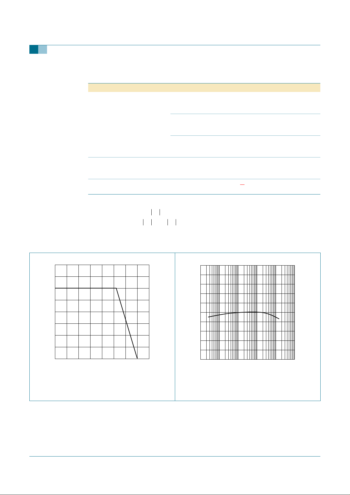
0 20015050 100
mra718
Ts (°C)
250
h
FE
200
150
100
50
0
−3
10
−2
−1
110
mra719
I
C
(mA)
10
1010
VCE = 6 V.
Fig 1. Power derating curve. Fig 2. DC current gain as a function of collector
current.
2
9397 750 13396 © Koninklijke Philips Electronics N.V. 2004. All rights reserved.
Product data sheet Rev. 03 — 20 July 2004 4 of 13
Page 5
Philips Semiconductors
BFR505
NPN 9 GHz wideband transistor
mra720
VCB (V)
C
(pF)
re
0.4
0.3
0.2
0.1
0
0108462
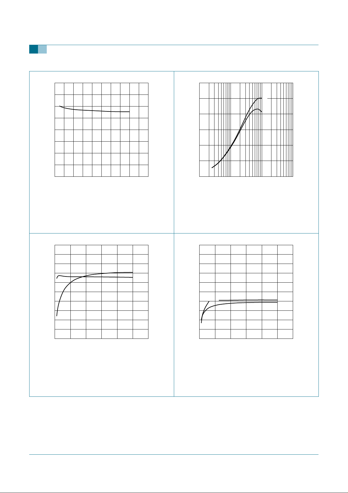
IC = 0 A; f = 1 MHz. T
Fig 3. Feedback capacitance as a function of
collector-base voltage.
25
gain
(dB)
20
15
mra764
(1)
(2)
I
C
(mA)
mra721
2
10
f
T
(GHz)
12
8
4
0
−1
10
= 25 °C; f = 1 GHz.
amb
(1)
(2)
101
(1) VCE= 6 V.
(2) VCE=3V.
Fig 4. Transition frequency as a function of collector
current.
25
gain
(dB)
20
15
mra765
10
5
0
01284
VCE = 6 V; f = 900 MHz.
(1) MSG.
(2) GUM.
IC (mA)
(1) MSG.
(2) G
(1) (2)
10
5
0
01284
VCE = 6 V; f = 2 GHz.
.
max
(3)
IC (mA)
(3) GUM.
Fig 5. Gain as a function of collector current. Fig 6. Gain as a function of collector current.
9397 750 13396 © Koninklijke Philips Electronics N.V. 2004. All rights reserved.
Product data sheet Rev. 03 — 20 July 2004 5 of 13
Page 6
Philips Semiconductors
BFR505
NPN 9 GHz wideband transistor
(3)
f (MHz)
mra766
50
gain
(dB)
40
30
20
10
4
0
10 10
(1)
(2)
2
10
3
10
f (MHz)
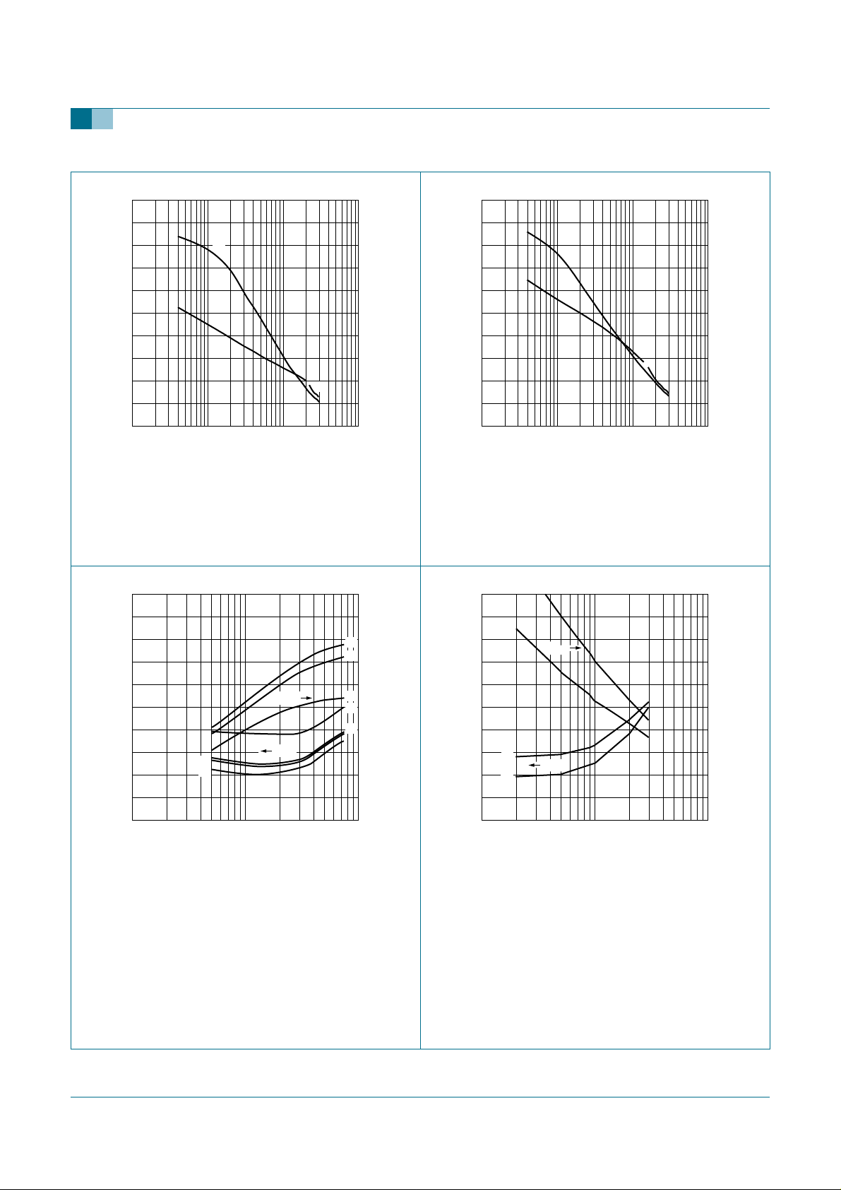
VCE = 6 V; IC = 5 mA.
(1) GUM.
(2) MSG.
(3) G
max
.
50
gain
(dB)
40
30
20
10
0
10 10
(1)
(2)
2
10
3
10
VCE = 6 V; IC = 1.25 mA.
(1) GUM.
(2) MSG.
(3) G
max
.
Fig 7. Gain as a function of frequency. Fig 8. Gain as a function of frequency.
mra726
20
G
ass
(dB)
15
(1)
(2)
F
min
(dB)
5
4
(1)
(2)
G
ass
F
min
(dB)
5
4
mra767
(3)
4
mra727
20
G
ass
(dB)
15
3
2
1
0
−1
VCE = 6 V.
(1) f = 900 MHz.
(2) f = 1000 MHz.
(3) f = 2000 MHz.
(4) f = 2000 MHz.
10
G
ass
F
(6)
(7)
min
1
I
(mA)
C
(3)
(4)
(5)
5
0
−5
1010
3
2
(3)
F
1
(4)
0
2
10
min
3
10
f (MHz)
VCE = 6 V.
(1) IC = 5 mA.
(2) IC = 1.25 mA.
(3) IC = 5 mA.
(4) IC = 1.25 mA.
10
5
0
−5
4
10
(5) f = 1000 MHz.
(6) f = 900 MHz.
(7) f = 500 MHz.
Fig 9. Minimum noise figure and associated available
gain as functions of collector current.
9397 750 13396 © Koninklijke Philips Electronics N.V. 2004. All rights reserved.
Fig 10. Minimum noise figure and associated available
gain as functions of frequency.
Product data sheet Rev. 03 — 20 July 2004 6 of 13
Page 7
Philips Semiconductors
BFR505
NPN 9 GHz wideband transistor
stability
circle
180°
+0.2
0
−0.2
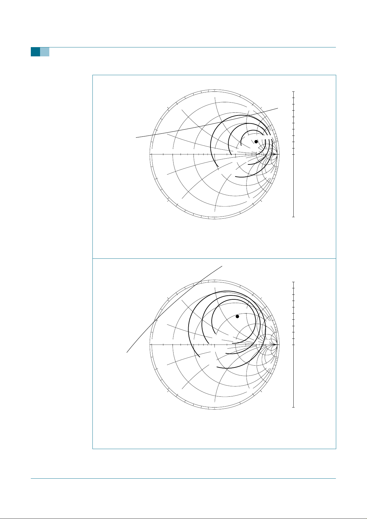
Zo = 50 Ω.
VCE = 6 V; IC = 5 mA; f = 900 MHz.
Fig 11. Noise circle figure.
pot. unst.
region
+0.5
−0.5
90°
+1
45°135°
+2
= 1.3 dB
min
Γ
opt
−2
+5
10
−5
−45°−135°
mra728
F
0.50.2
1
F = 3 dB
−1
−90°
F = 1.5 dB
2
F = 2 dB
1.0
0.8
0.6
0.4
0.2
0°
0
1.0
pot. unst.
region
180°
+0.2
0
−0.2
stability
circle
Zo = 50 Ω.
VCE = 6 V; IC = 5 mA; f = 2000 MHz.
Fig 12. Noise circle figure.
+0.5
−0.5
0.50.2
F = 3 dB
F = 4 dB
−90°
90°
+1
F
F = 2.5 dB
1
−1
= 1.9 dB
min
Γ
1.0
45°135°
+2
opt
2
−2
+5
5
10
−5
−45°−135°
mra729
0.8
0.6
0.4
0.2
0°
0
1.0
9397 750 13396 © Koninklijke Philips Electronics N.V. 2004. All rights reserved.
Product data sheet Rev. 03 — 20 July 2004 7 of 13
Page 8
Philips Semiconductors
BFR505
NPN 9 GHz wideband transistor
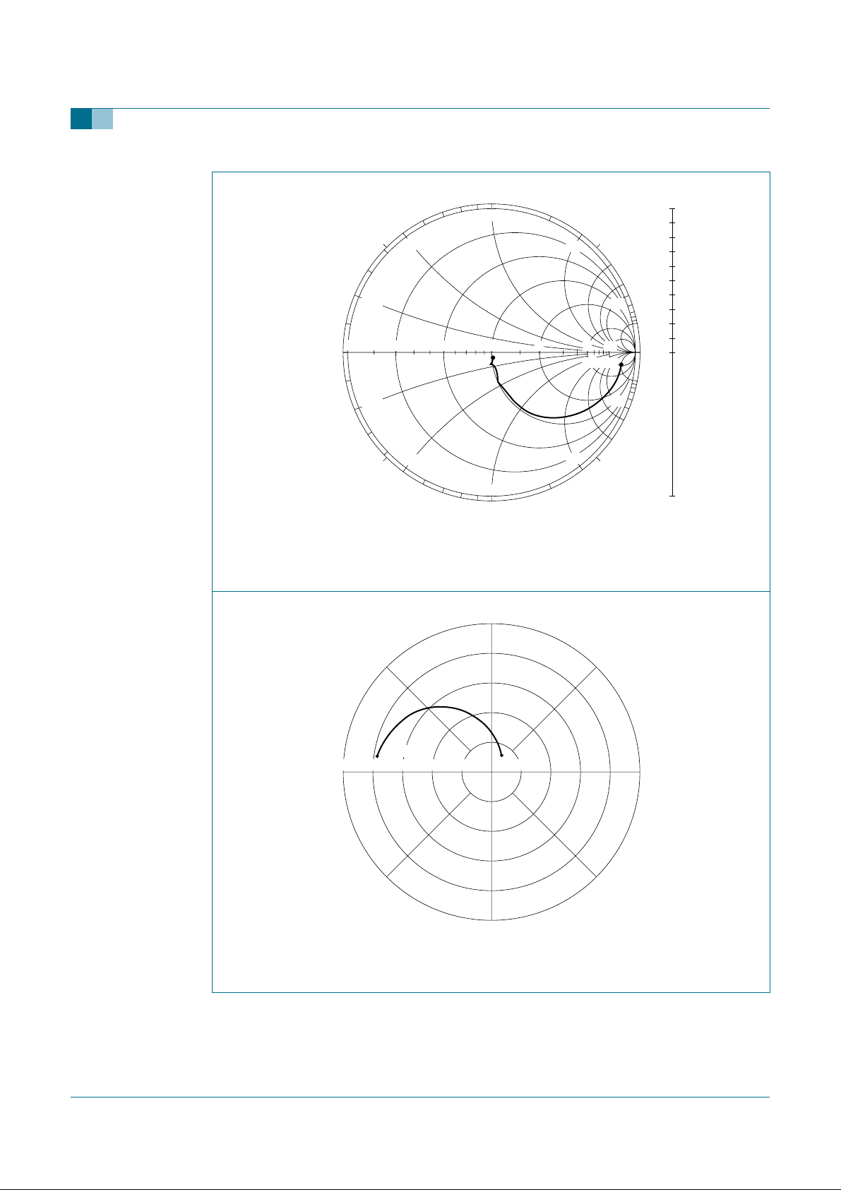
90°
+1
+0.5
+0.2
180°
0
−0.2
0.50.2
−0.5
3 GHz
1
−1
−90°
2
Zo = 50 Ω.
VCE = 6 V; IC = 5 mA.
Fig 13. Common emitter input reflection coefficient (S11).
+2
−2
45°135°
5
10
40 MHz
−45°−135°
+5
−5
mra722
1.0
0.8
0.6
0.4
0.2
0°
0
1.0
90°
15 12 9 6 3
180°
40 MHz
3 GHz
−90°
VCE = 6 V; IC = 5 mA.
Fig 14. Common emitter forward transmission coefficient (S21).
45°135°
0°
−45°−135°
mra723
9397 750 13396 © Koninklijke Philips Electronics N.V. 2004. All rights reserved.
Product data sheet Rev. 03 — 20 July 2004 8 of 13
Page 9
Philips Semiconductors
BFR505
NPN 9 GHz wideband transistor
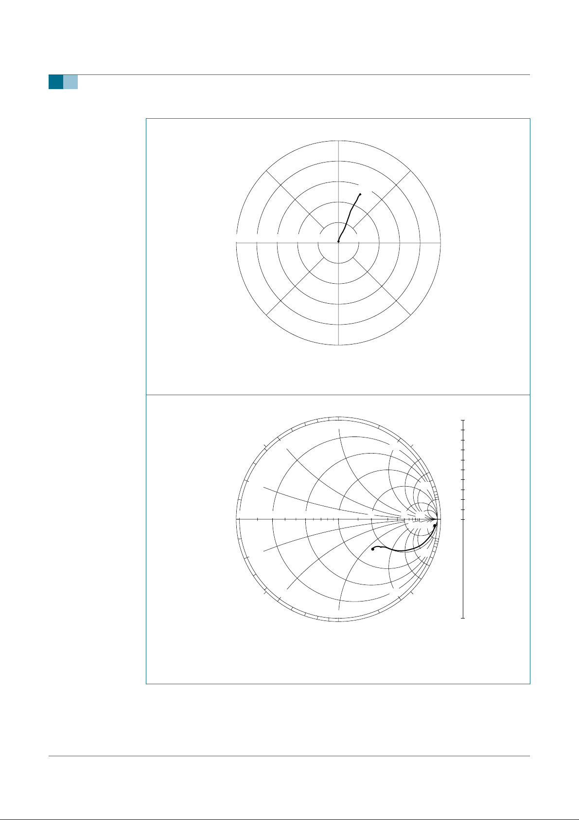
90°
45°135°
3 GHz
0.5 0.4 0.3 0.2 0.1 40 MHz
180°
−90°
VCE = 6 V; IC = 5 mA.
Fig 15. Common emitter reverse transmission coefficient (S12).
90°
+1
180°
+0.5
+0.2
0
0.50.2
1
+2
2
5
−45°−135°
45°135°
+5
10
40 MHz
mra724
0°
1.0
0.8
0.6
0.4
0.2
0°
0
−2
−5
−45°−135°
1.0
mra725
−0.2
3 GHz
−0.5
−1
−90°
Zo = 50 Ω.
VCE = 6 V; IC = 5 mA.
Fig 16. Common emitter output reflection coefficient (S22).
9397 750 13396 © Koninklijke Philips Electronics N.V. 2004. All rights reserved.
Product data sheet Rev. 03 — 20 July 2004 9 of 13
Page 10
Philips Semiconductors
BFR505
NPN 9 GHz wideband transistor
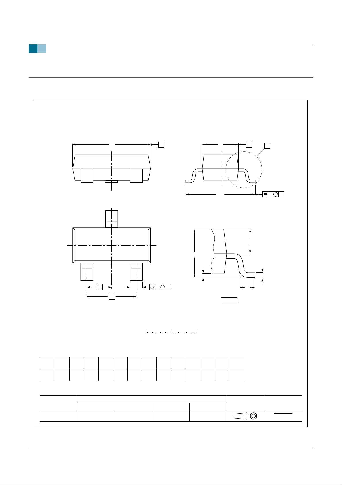
8. Package outline
Plastic surface mounted package; 3 leads SOT23
D
3
A
A
1
12
e
1
b
p
e
w M
B
E
H
E
detail X
AB
Q
L
p
X
v M
A
c
0 1 2 mm
scale
DIMENSIONS (mm are the original dimensions)
A
1.1
0.9
1
A
max.
0.48
0.1
0.38
cD
b
p
0.15
0.09
IEC JEDEC EIAJ
3.0
2.8
E
1.4
1.2
REFERENCES
1.9
e
e
1
0.95
H
2.5
2.1
L
Qwv
p
E
0.55
0.45
0.15
0.45
0.2
0.1
EUROPEAN
PROJECTION
ISSUE DATE
97-02-28
99-09-13
UNIT
mm
OUTLINE
VERSION
SOT23 TO-236AB
Fig 17. Package outline.
9397 750 13396 © Koninklijke Philips Electronics N.V. 2004. All rights reserved.
Product data sheet Rev. 03 — 20 July 2004 10 of 13
Page 11

Philips Semiconductors
NPN 9 GHz wideband transistor
BFR505
9. Revision history
Table 8: Revision history
Document ID Release date Data sheet status Change notice Order number Supersedes
BFR505_3 20040720 Product data 9397 750 13396 BFR505_CNV_2
Modifications:
BFR505_CNV_2 19971204 Product specification - - -
• Marking code added Table4.
• Data sheet updated to latest standards.
9397 750 13396 © Koninklijke Philips Electronics N.V. 2004. All rights reserved.
Product data sheet Rev. 03 — 20 July 2004 11 of 13
Page 12

Philips Semiconductors
10. Data sheet status
BFR505
NPN 9 GHz wideband transistor
Level Data sheet status
I Objective data Development This data sheet contains data from the objective specification for product development. Philips
II Preliminary data Qualification This data sheet contains datafrom the preliminary specification. Supplementary datawill be published
III Product data Production This data sheet contains data from the product specification. Philips Semiconductors reserves the
[1] Please consult the most recently issued data sheet before initiating or completing a design.
[2] The product status of the device(s) described in this data sheet may have changed since this data sheet was published. The latest information is available on the Internet at
URL http://www.semiconductors.philips.com.
[3] For data sheets describing multiple type numbers, the highest-level product status determines the data sheet status.
[1]
Product status
11. Definitions
Short-form specification — The data in a short-form specification is
extracted from a full data sheet with the same type number and title. For
detailed information see the relevant data sheet or data handbook.
Limiting values definition — Limiting values given are in accordance with
the Absolute Maximum Rating System (IEC 60134). Stress above one or
more of the limiting values may cause permanent damage to the device.
These are stress ratings only and operation of the device at these or at any
other conditions above those given in the Characteristics sections of the
specification is not implied. Exposure to limiting values for extended periods
may affect device reliability.
Application information — Applications that are described herein for any
of these products are for illustrative purposes only. Philips Semiconductors
make no representationor warranty that such applications will be suitable for
the specified use without further testing or modification.
[2] [3]
Definition
Semiconductors reserves the right to change the specification in any manner without notice.
at a later date.Philips Semiconductorsreserves the right tochange thespecification withoutnotice, in
order to improve the design and supply the best possible product.
right to makechanges atany time in order toimprove the design, manufacturing and supply. Relevant
changes will be communicated via a Customer Product/Process Change Notification (CPCN).
12. Disclaimers
Life support — These products are not designed for use in life support
appliances, devices, or systems where malfunction of these products can
reasonably be expected to result in personal injury. Philips Semiconductors
customers using or selling these products for use in such applications do so
at their own risk and agree to fully indemnify Philips Semiconductors for any
damages resulting from such application.
Right to make changes — Philips Semiconductors reserves the right to
make changes in the products - including circuits, standard cells, and/or
software - described or contained herein in order to improve design and/or
performance. When the product is in full production (status ‘Production’),
relevant changes will be communicated via a Customer Product/Process
Change Notification (CPCN). Philips Semiconductors assumes no
responsibility or liability for the use of any of these products, conveys no
license or title under any patent, copyright, or mask work right to these
products, and makes no representations or warranties that these products are
free from patent, copyright, or maskwork right infringement, unless otherwise
specified.
13. Contact information
For additional information, please visit: http://www.semiconductors.philips.com
For sales office addresses, send an email to: [email protected]
9397 750 13396 © Koninklijke Philips Electronics N.V. 2004. All rights reserved.
Product data sheet Rev. 03 — 20 July 2004 12 of 13
Page 13

Philips Semiconductors
14. Contents
1 Product profile . . . . . . . . . . . . . . . . . . . . . . . . . . 1
1.1 General description. . . . . . . . . . . . . . . . . . . . . . 1
1.2 Features . . . . . . . . . . . . . . . . . . . . . . . . . . . . . . 1
1.3 Quick reference data. . . . . . . . . . . . . . . . . . . . . 1
2 Pinning information. . . . . . . . . . . . . . . . . . . . . . 2
3 Ordering information. . . . . . . . . . . . . . . . . . . . . 2
4 Marking. . . . . . . . . . . . . . . . . . . . . . . . . . . . . . . . 2
5 Limiting values. . . . . . . . . . . . . . . . . . . . . . . . . . 3
6 Thermal characteristics. . . . . . . . . . . . . . . . . . . 3
7 Characteristics. . . . . . . . . . . . . . . . . . . . . . . . . . 3
8 Package outline . . . . . . . . . . . . . . . . . . . . . . . . 10
9 Revision history. . . . . . . . . . . . . . . . . . . . . . . . 11
10 Data sheet status. . . . . . . . . . . . . . . . . . . . . . . 12
11 Definitions . . . . . . . . . . . . . . . . . . . . . . . . . . . . 12
12 Disclaimers. . . . . . . . . . . . . . . . . . . . . . . . . . . . 12
13 Contact information . . . . . . . . . . . . . . . . . . . . 12
BFR505
NPN 9 GHz wideband transistor
© Koninklijke Philips Electronics N.V. 2004
All rights are reserved. Reproduction in whole or in part is prohibited without the prior
written consent of the copyright owner. The information presented in this document does
not form part ofany quotationor contract, is believed to be accurateand reliableand may
be changed without notice. No liability will be accepted by the publisher for any
consequence of its use. Publication thereof does not convey nor imply any license under
patent- or other industrial or intellectual property rights.
Document order number: 9397 750 13396
Published in The Netherlands
Date of release: 20 July 2004
 Loading...