

Page 1

DATA SH EET
DISCRETE SEMICONDUCTORS
BFG97
NPN 5 GHz wideband transistor
Product specification September 1995
Page 2
NXP Semiconductors Product specification
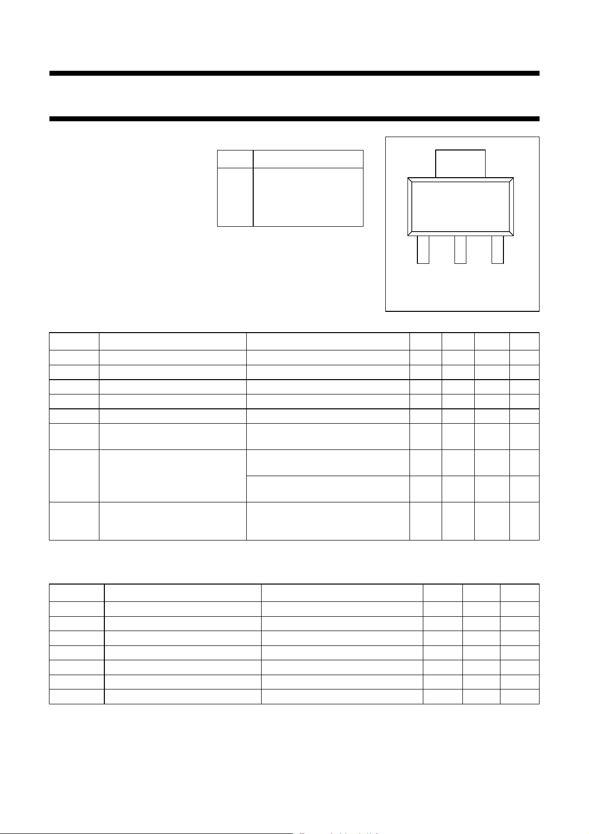
Fig.1 SOT223.
4
123
MSB002 - 1
Top view
NPN 5 GHz wideband transistor BFG97
DESCRIPTION
NPN planar epitaxial transistor
mounted in a plastic SOT223
envelope.
It features excellent output voltage
capabilities, and is primarily intended
for use in MATV applications.
PINNING
PIN DESCRIPTION
1emitter
2 base
3emitter
4 collector
PNP complement is the BFG31.
QUICK REFERENCE DATA
SYMBOL PARAMETER CONDITIONS MIN. TYP. MAX. UNIT
V
V
I
P
h
f
G
V
CBO
CEO
C
tot
FE
T
UM
o
collector-base voltage open emitter 20 V
collector-emitter voltage open base 15 V
DC collector current 100 mA
total power dissipation up to Ts=125 C (note 1) 1W
DC current gain IC=70 mA; VCE=10 V; Tj=25 C25 80
transition frequency IC=70 mA; VCE=10 V;
f = 500 MHz; T
amb
=25 C
maximum unilateral power gain IC=70 mA; VCE=10 V;
f = 500 MHz; T
I
=70 mA; VCE=10 V;
C
f = 800 MHz; T
amb
amb
=25 C
=25 C
output voltage IC=70 mA; VCE=10 V;
60 dB; RL=75 ;
d
im =
f
=793.25 MHz;T
(pqr)
amb
=25 C
5.5 GHz
16 dB
12 dB
700 mV
LIMITING VALUES
In accordance with the Absolute Maximum System (IEC 134) .
SYMBOL PARAMETER CONDITIONS MIN. MAX. UNIT
V
CBO
V
CEO
V
EBO
I
C
P
tot
T
stg
T
j
Note
is the temperature at the soldering point of the collector tab.
1. T
s
collector-base voltage open emitter 20 V
collector-emitter voltage open base 15 V
emitter-base voltage open collector 3V
DC collector current 100 mA
total power dissipation up to Ts=125 C (note 1) 1W
storage temperature 65 150 C
junction temperature 175 C
September 1995 2
Page 3
NXP Semiconductors Product specification
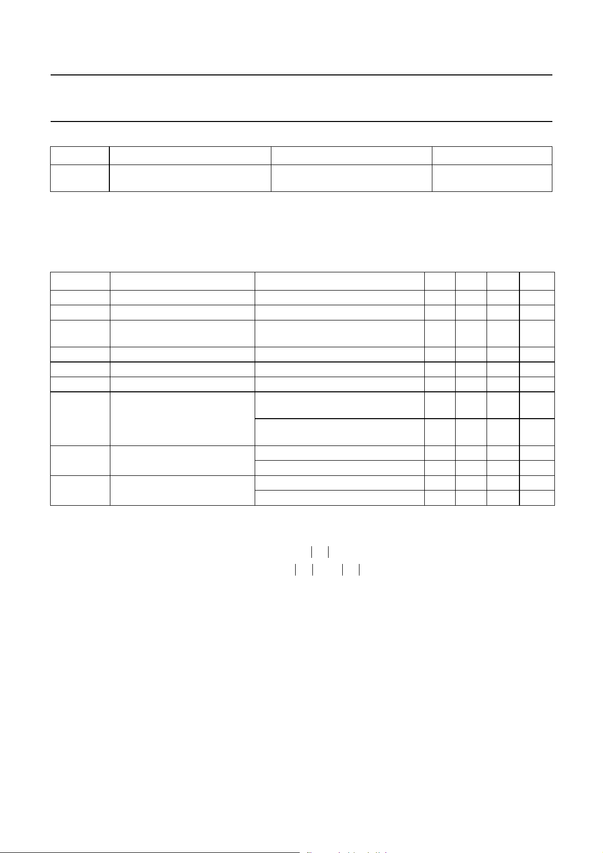
G
UM
10 log
S
21
2
1S
11
2
–1S
22
2
–
----------------------------------------------------------
dB.=
NPN 5 GHz wideband transistor BFG97
THERMAL RESISTANCE
SYMBOL PARAMETER CONDITIONS THERMAL RESISTANCE
R
th j-s
Note
is the temperature at the soldering point of the collector tab.
1. T
s
CHARACTERISTICS
=25 C unless otherwise specified.
T
j
SYMBOL PARAMETER CONDITIONS MIN. TYP. MAX. UNIT
I
CBO
h
FE
f
T
C
c
C
e
C
re
G
UM
V
o
d
2
thermal resistance from junction to
up to Ts=125 C (note 1) 50 K/W
soldering point
collector cut-off current IE=0; VCB=10 V 100 nA
DC current gain IC=70 mA; VCE= 10 V 25 80
transition frequency IC=70 mA; VCE= 10 V;
f = 500 MHz; T
amb
=25 C
5.5 GHz
collector capacitance IE=ie= 0; VCB=10 V; f=1 MHz 1.5 pF
emitter capacitance IC=ic=0; VEB=0.5 V; f=1 MHz 6.5 pF
feedback capacitance IC=0; VCE= 10 V; f = 1 MHz 1 pF
maximum unilateral power gain
(note 1)
IC=70 mA; VCE= 10 V;
f = 500 MHz; T
=70 mA; VCE= 10 V;
I
C
f = 800 MHz; T
amb
amb
=25 C
=25 C
16 dB
12 dB
output voltage note 2 750 mV
note 3 700 mV
second order intermodulation
distortion
note 4 56 dB
note 5 53 dB
Notes
1. G
2. d
3. d
4. I
5. I
is the maximum unilateral power gain, assuming S12is zero and
UM
= 60 dB (DIN 45004B); IC=70 mA; VCE=10 V; RL= 75 ; T
im
V
V
V
measured at f
V
V
V
measured at f
V
C
V
at dim= 60 dB;
p=Vo
6 dB; fp= 445.25 MHz;
q=Vo
6 dB; fq= 453.25 MHz; fr= 455.25 MHz;
r=Vo
= 443.25 MHz.
(pqr)
= 60 dB (DIN 45004B); IC=70 mA; VCE=10 V; RL= 75 ; T
im
at dim= 60 dB;
p=Vo
6 dB; fp= 795.25 MHz;
q=Vo
6 dB; fq= 803.25 MHz; fr= 805.25 MHz;
r=Vo
= 793.25 MHz.
(pqr)
=70 mA; VCE=10 V; RL=75 ; T
C
p=Vq=Vo
= 50 dBmV; f
= 450 MHz; fp=50 MHz; fq=400 MHz.
(pq)
=70 mA; VCE=10 V; RL= 75 ; T
p=Vq=Vo
= 50 dBmV; f
= 810 MHz; fp=250 MHz; fq=560 MHz.
(pq)
amb
amb
=25 C;
=25 C;
amb
amb
=25 C
=25 C
September 1995 3
Page 4
NXP Semiconductors Product specification
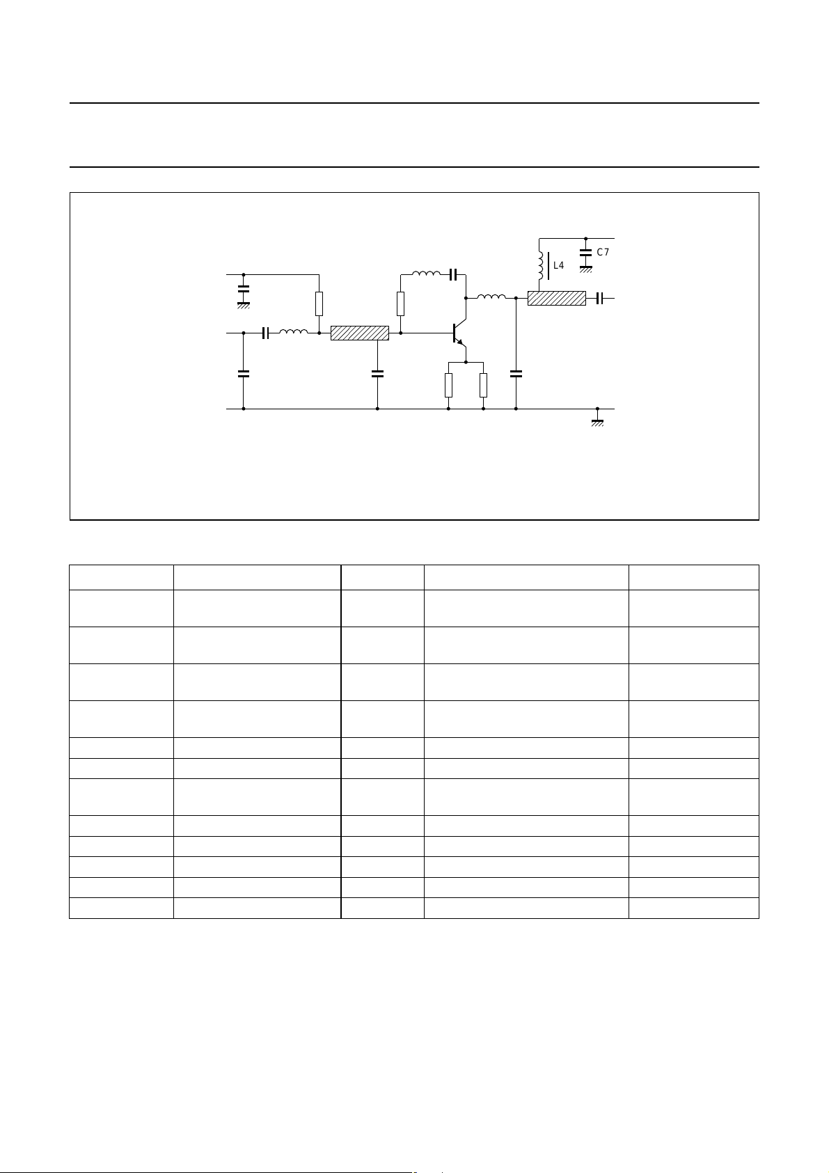
Fig.2 Intermodulation distortion and second order intermodula tio n distortion test circuit.
handbook, full pagewidth
MBB807
L1C1
output
75 Ω
DUT
input
75 Ω
V
CC
V
BB
L4
C7
C8L6
L5
C4
L2
R2
C5
R3 R4
C6
R1
L3
C3
C2
NPN 5 GHz wideband transistor BFG97
List of components (see test circuit)
DESIGNATION DESCRIPTION VALUE DIMENSIONS CATALOGUE NO.
C2, C3, C7, C8 multilayer ceramic
C1, C4, C6 multilayer ceramic
C5 (note 1) miniature ceramic plat e
L1 (note 1) 0.5 turns 0.4 mm copper
L2 microstripline 75 length 14 mm; width 2.5 mm
L3 microstripline 75 length 8 mm; width 2.5 mm
L4, L5 (note 1) 1.5 turns 0.4 mm copper
L6 microstripline 75 length 19 mm; width 2.5 mm
L7 Ferroxcube choke 5 H 3122 108 20153
R1 metal film resistor 10 k 2322 180 73103
R2 (note 1) metal film resistor 220 2322 180 73221
R3, R4 metal film resistor 30 2322 180 73309
Notes
The circuit has been built on a double copper-clad printed circuit board with PTFE dielectric (
thickness of copper sheet 2 35 m.
1. Components C5, L1, L4, L5, and R2 are mounted on the underside of the PCB.
September 1995 4
capacitor
capacitor
capacitor
wire
wire
10 nF 2222 590 08627
1.2 pF 2222 851 12128
10 nF 2222 629 08103
int. dia. 3 mm
int. dia. 3 mm;
winding pitch 1 mm
= 2.2); thickness
r
1
16
inch;
Page 5
NXP Semiconductors Product specification
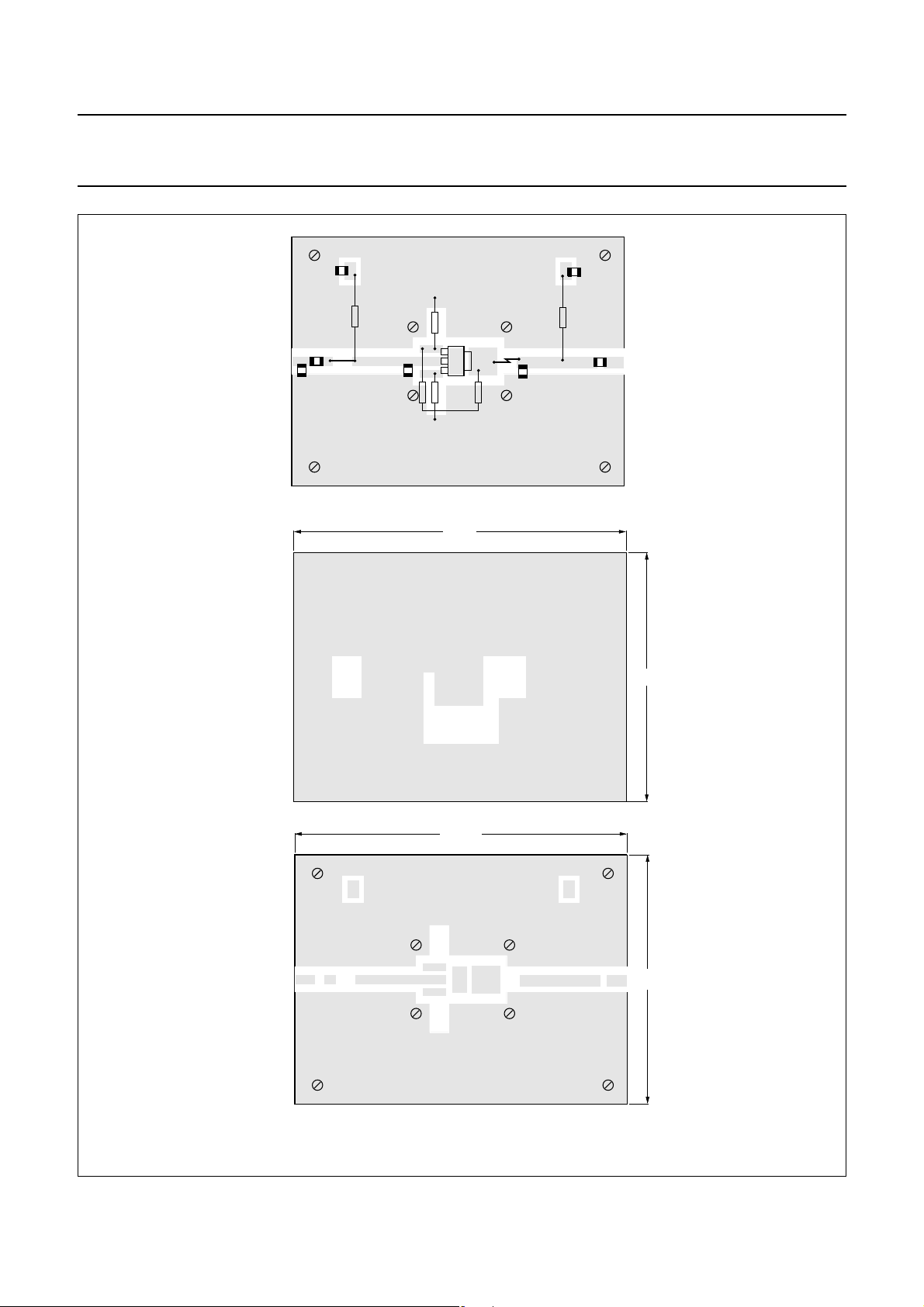
Fig.3 Intermodulation distortion and second order intermodu l ation distortion printed circuit board.
handbook, full pagewidth
MEA970
80 mm
60 mm
mounting
screws
M 2.5 (8x)
handbook, full pagewidth
MEA969
60 mm
80 mm
handbook, full pagewidth
MEA971
75
input
75
output
C8
C7
L7
V
CC
V
BB
R1
C3
C2
C1
L2
L6
R3
R2
R4
C5
L4
L5
L1
L3
C6
C4
Ω
Ω
NPN 5 GHz wideband transistor BFG97
September 1995 5
Page 6
NXP Semiconductors Product specification
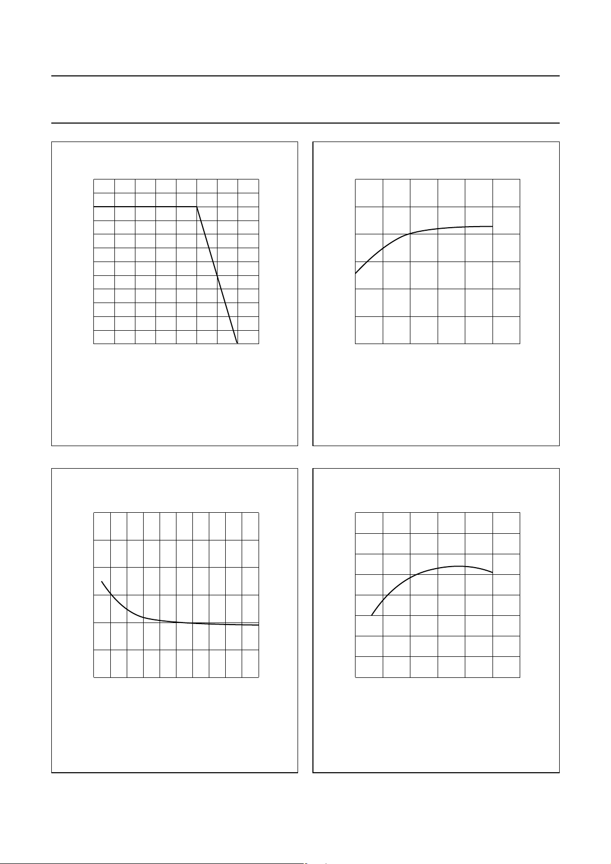
Fig.4 Power derating curve.
handbook, halfpage
0 50 100 200
0.8
0.6
0.2
0
0.4
MBB797
150
T ( C)
o
s
P
tot
(W)
1.0
1.2
Fig.5 DC current gain as a function of collector
current.
VCE= 10 V; Tj=25 C.
handbook, halfpage
0
120
80
40
0
40 120
MBB774
80
I (mA)
C
h
FE
Fig.6 Feedback capacitance as a function of
collector-emitter voltage.
IE= 0; f = 1 MHz; Tj=25 C.
handbook, halfpage
V (V)
CE
MBB798
0
3
2
1
0
10 20
C
re
(pF)
Fig.7 Transition frequency as a function of
collector current.
VCE= 10 V; f = 500 MHz; Tj=25 C.
handbook, halfpage
04080
8
6
2
0
4
MBB773
120
I (mA)
C
(GHz)
T
f
NPN 5 GHz wideband transistor BFG97
September 1995 6
Page 7
NXP Semiconductors Product specification
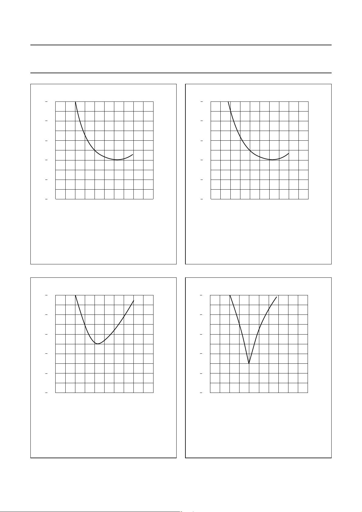
Fig.8 Intermodulation distortion as a function of
collector current.
VCE= 10 V; Vo=750 mV; f
(pqr)
= 443.25 MHz;
T
amb
=25 C.
handbook, halfpage
20 120
45
70
65
MBB799
60
55
50
40 60 80 100
d
im
(dB)
I (mA)
C
Fig.9 Intermodulation distortion as a function of
collector current.
VCE= 10 V; Vo=700 mV; f
(pqr)
= 793.25 MHz;
T
amb
=25 C.
handbook, halfpage
MBB796
20 120
45
70
65
60
55
50
40 60 80 100
d
im
(dB)
I (mA)
C
Fig.10 Second order intermodulation distortion as
a function of collector current.
VCE= 10 V; Vo=50 dBmV; f
(pq)
= 450 MHz;
T
amb
=25 C.
handbook, halfpage
MBB800
20 120
45
70
65
60
55
50
40 60 80 100
d
2
(dB)
I (mA)
C
Fig.11 Second order intermodulation distortion as
a function of collector current.
VCE= 10 V; Vo=50 dBmV; f
(pq)
= 810 MHz;
T
amb
=25 C.
handbook, halfpage
MBB801
20 120
45
70
65
60
55
50
40 60 80 100
d
2
(dB)
I (mA)
C
NPN 5 GHz wideband transistor BFG97
September 1995 7
Page 8
NXP Semiconductors Product specification
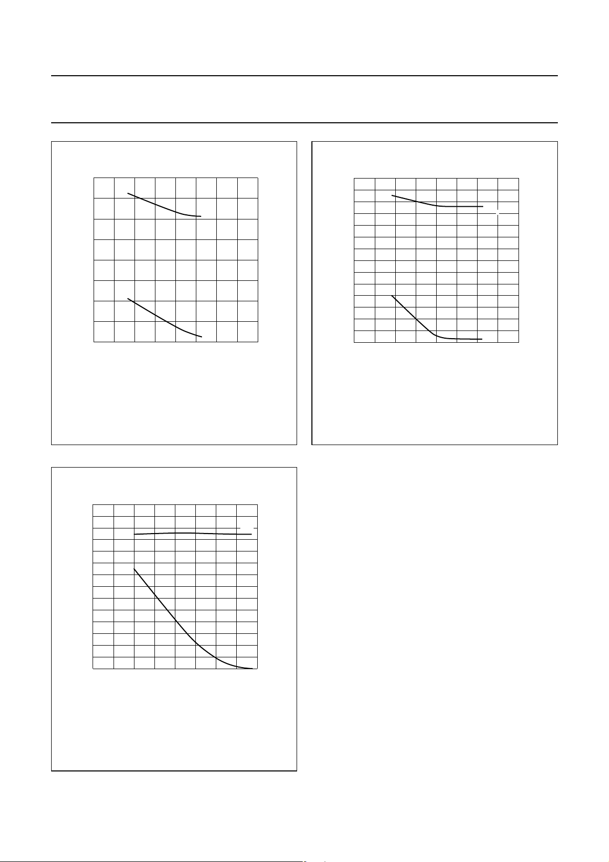
Fig.12 Load impedance as a fun ction of output
power.
VCE= 6 V; f = 900 MHz.
handbook, halfpage
0 0.25
1
–20
0
20
MEA963
0.50
P
OUT
(W)
10
30
0.75
40
Z
(Ω)
L
50
60
R
L
X
L
–10
Fig.13 Load impedance as a fun ction of output
power.
VCE= 7.5 V; f = 900 MHz.
handbook, halfpage
0 0.25
1
0
20
MEA964
0.50
P
OUT
(W)
10
30
0.75
40
Z
(Ω)
L
50
60
X
L
–10
R
L
Fig.14 Load impedance as a fun ction of output
power.
VCE= 10 V; f = 900 MHz.
handbook, halfpage
0 0.25
1
0
20
MEA965
0.50
P
OUT
(W)
10
30
0.75
40
Z
(Ω)
L
50
60
X
L
–10
R
L
NPN 5 GHz wideband transistor BFG97
September 1995 8
Page 9
NXP Semiconductors Product specification
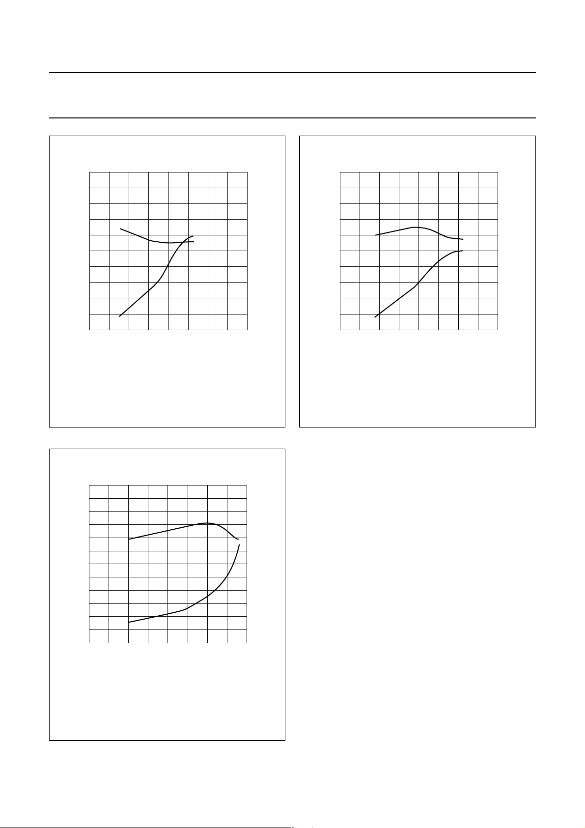
Fig.15 Input impedance as a function of output
power.
VCE= 6 V; f = 900 MHz.
handbook, halfpage
0 0.25
1
–5
0
10
MEA957
0.50
P
OUT
(W)
5
15
0.75
20
Z
(Ω)
i
r
i
x
i
Fig.16 Input impedance as a function of output
power.
VCE= 7.5 V; f = 900 MHz.
handbook, halfpage
0 0.25
1
–5
0
10
MEA958
0.50
P
OUT
(W)
5
15
0.75
20
Z
(Ω)
i
r
i
x
i
Fig.17 Input impedance as a function of output
power.
VCE= 10 V; f = 900 MHz.
handbook, halfpage
0 0.25
1
–10
0
10
MEA959
0.50
P
OUT
(W)
5
15
0.75
20
Z
(Ω)
i
r
i
x
i
5
NPN 5 GHz wideband transistor BFG97
September 1995 9
Page 10
NXP Semiconductors Product specification
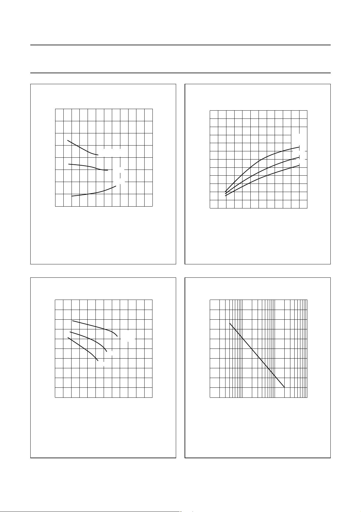
Fig.18 Efficiency as a function of output power.
f = 900 MHz.
handbook, halfpage
0 0.5 1.5
40
50
70
MEA961
1
η
(%)
P
OUT
(W)
V =CE6 V
60
80
10 V
7.5 V
Fig.19 Output power as a function of input power.
f = 900 MHz.
handbook, halfpage
0 100 300
1.5
0
0.5
1
MEA962
200
P
OUT
(W)
PIN(mW)
V =
CE
10 V
6 V
7.5 V
Fig.20 Power gain as a function of output power.
f = 900 MHz.
handbook, halfpage
0 0.5 1.5
10
0
2
6
MEA960
1
G
p
(dB)
P
OUT
(W)
4
8
V =
CE
10 V
6 V
7.5 V
Fig.21 Maximum unilateral powe r gain as a
function of frequency.
IC=70 mA; VCE=10 V; T
amb
=25 C.
handbook, halfpage
50
0
20
30
10
MBB802
10
2
10
3
10
4
10
f (MHz)
G
UM
(dB)
40
NPN 5 GHz wideband transistor BFG97
September 1995 10
Page 11
NXP Semiconductors Product specification
handbook, full pagewidth
MBB803
10
25
50
100
250
10
25
50
100
250
0
+ j
– j
2 GHz
10 25 50 100 250
40 MHz
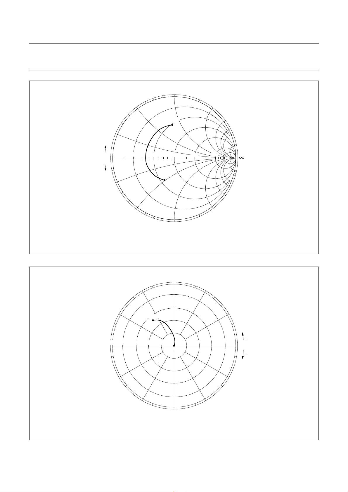
Fig.22 Common emitter input reflection coefficient (S11).
IC=70 mA; VCE=10 V; T
amb
=25 C.
Zo= 50 .
handbook, full pagewidth
MBB806
180
ϕ
ϕ
0
o
30
o
60
o
90
o
120
o
150
o
o
150
o
120
o
90
o
60
o
30
o
80 40100 60 20
2 GHz
40 MHz
Fig.23 Common emitter forward transmission coefficient (S21).
IC=70 mA; VCE=10 V; T
amb
=25 C.
NPN 5 GHz wideband transistor BFG97
September 1995 11
Page 12
NXP Semiconductors Product specification
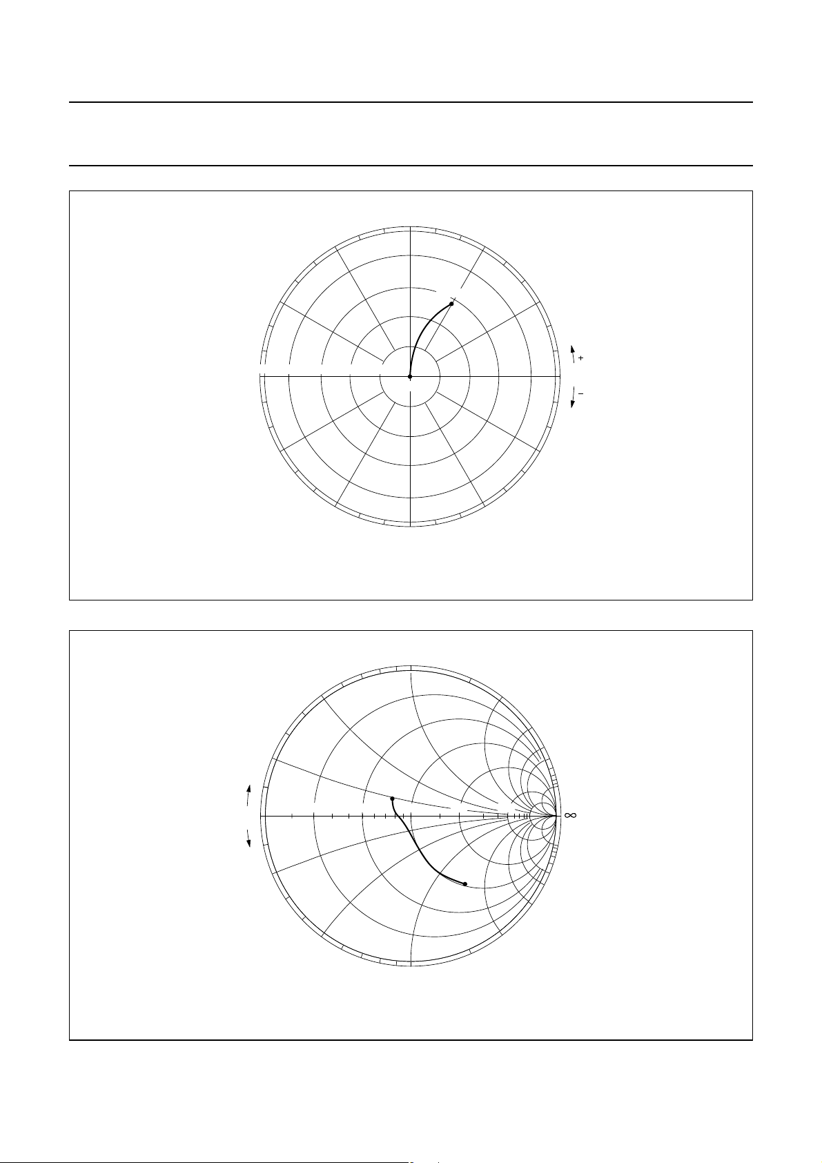
Fig.24 Common emitter reverse transmission coefficient (S12).
IC=70 mA; VCE=10 V; T
amb
=25 C.
handbook, full pagewidth
MBB805
180
ϕ
ϕ
0
o
30
o
60
o
90
o
120
o
150
o
o
150
o
120
o
90
o
60
o
30
o
0.4 0.20.5 0.3 0.1
2 GHz
40 MHz
handbook, full pagewidth
MBB804
10
25
50
100
250
10
25
50
100
250
0
+ j
– j
40 MHz
2 GHz
10 25 50 100 250
Fig.25 Common emitter output reflection coefficient (S22).
IC=70 mA; VCE=10 V; T
amb
=25 C.
Z
o
= 50 .
NPN 5 GHz wideband transistor BFG97
September 1995 12
Page 13
NXP Semiconductors Product specification
UNIT A1b
p
cD
E
e1HEL
p
Qywv
REFERENCES
OUTLINE
VERSION
EUROPEAN
PROJECTION
ISSUE DATE
IEC JEDEC JEITA
mm
0.10
0.01
1.8
1.5
0.80
0.60
b
1
3.1
2.9
0.32
0.22
6.7
6.3
3.7
3.3
2.3
e
4.6
7.3
6.7
1.1
0.7
0.95
0.85
0.1 0.10.2
DIMENSIONS (mm are the original dimensions)
SOT223 SC-73
04-11-10
06-03-16
w M
b
p
D
b
1
e
1
e
A
A
1
L
p
Q
detail X
H
E
E
v M
A
AB
B
c
y
0 2 4 mm
scale
A
X
132
4
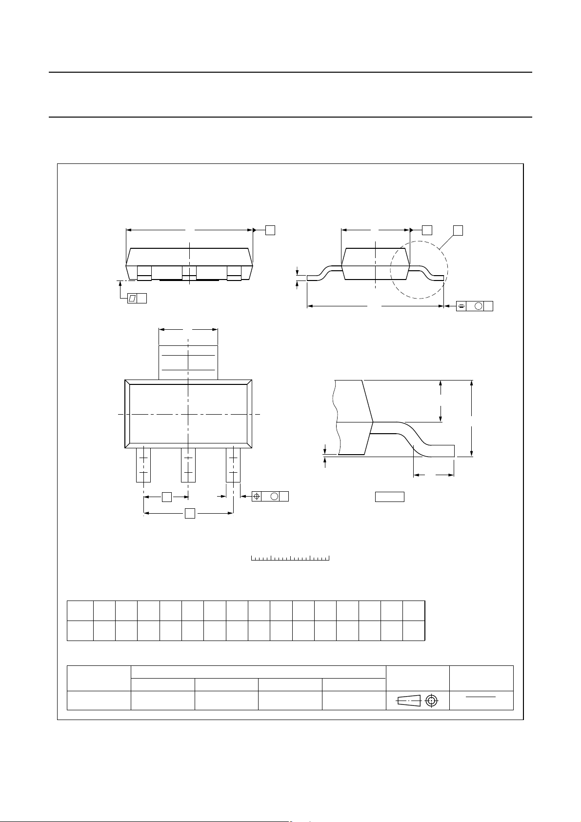
Plastic surface-mounted package with increased heatsink; 4 leads SOT223
NPN 5 GHz wideband transistor BFG97
PACKAGE OUTLINE
September 1995 13
Page 14

NXP Semiconductors Product specification
NPN 5 GHz wideband transistor BFG97
DATA SHEET STATUS
DOCUMENT
STATUS
Objective data sheet Development This document contains data from the objective specification for product
Preliminary data sheet Qualification This document contains data from the preliminary specification.
Product data sheet Production This document contains the product specification.
Notes
1. Please consult the most recently issued document before initiating or completing a design.
2. The product status of device(s) desc ribed in this document may have changed since this document was published
and may differ in case of multiple devices. The latest product status information is available on the Internet at
URL http://www.nxp.com.
DEFINITIONS
Product specification The information and data
provided in a Product data sheet shall define the
specification of the product as agreed between NXP
Semiconductors and its customer, unless NXP
Semiconductors and customer have explicitly agreed
otherwise in writing. In no event however, shall an
agreement be valid in which the NXP Semiconductors
product is deemed to offer functions and qualities beyond
those described in the Product data sheet.
DISCLAIMERS
Limited warranty and liability Information in this
document is believed to be accurate and reliable.
However, NXP Semiconductors does not give any
representations or warranties, expressed or implied, as to
the accuracy or completeness of such information and
shall have no liability for the consequences of use of such
information.
In no event shall NXP Semiconductors be liable for any
indirect, incidental, punitive, special or consequential
damages (including - without limitation - lost profits, lost
savings, business interruption, costs related to the
removal or replacement of any products or rework
charges) whether or not such damages are based on tort
(including negligence), warranty, breach of contract or any
other legal theory.
Notwithstanding any damages that customer might incur
for any reason whatsoever, NXP Semiconductors’
aggregate and cumulative liability towards customer for
the products described herein shall be limited in
accordance with the Terms and conditions of commercial
sale of NXP Semiconductors.
(1)
PRODUCT
STATUS
(2)
DEFINITION
development.
Right to make changes NXP Semiconductors
reserves the right to make changes to information
published in this document, including without limitation
specifications and product descriptions, at any time and
without notice. This document supersedes and replaces all
information supplied prior to the publication he reof.
Suitability for use NXP Semiconductors products are
not designed, authorized or warranted to be suitable for
use in life support, life-critical or safety-critical systems or
equipment, nor in applications wher e failure or malfunction
of an NXP Semiconductors product can reasonably be
expected to result in personal injury, death or severe
property or environmental damage. NXP Semiconductors
accepts no liability for inclusion and/or use of NXP
Semiconductors products in such equipment or
applications and therefore such inc l usion and/or use is at
the customer’s own risk.
Applications Applications that ar e described herein for
any of these products are for illustrative purposes only.
NXP Semiconductors makes no representation or
warranty that such applications will be suitable for the
specified use without further testing or modification.
Customers are responsible for the design and operation of
their applications and products using NXP
Semiconductors products, and NXP Semiconductors
accepts no liability for any assistance with applications or
customer product design. It is customer’s sole
responsibility to determine whether the NXP
Semiconductors product is suitable and fit for the
customer’s applications and products planned, as well as
for the planned application and use of customer’s third
party customer(s). Customers should provide appropriate
design and operating safeguards to minimize the ris ks
associated with their applications and products.
September 1995 14
Page 15

NXP Semiconductors Product specification
NPN 5 GHz wideband transistor BFG97
NXP Semiconductors does not accept any liability related
to any default, damage, costs or problem which is based
on any weakness or default in the customer’s applications
or products, or the application or use by customer’s third
party customer(s). Customer is responsible for doing all
necessary testing for the customer’s applicat ions and
products using NXP Semiconductors products in or de r to
avoid a default of the applications and the prod ucts or of
the application or use by customer’s third party
customer(s). NXP does not accept any liability in this
respect.
Limiting values Stress above one or more limiting
values (as defined in the Absolute Maximum Ratings
System of IEC 60134) will cause permanent damage to
the device. Limiting values are stress ratings only and
(proper) operation of the device at these or any other
conditions above those given in the Rec ommended
operating conditions section (if present) or the
Characteristics sections of this document is not warranted.
Constant or repeated exposure to limiting values will
permanently and irreversibly affect the quality and
reliability of the device.
Terms and conditions of commercial sale NXP
Semiconductors products are sold subject to the general
terms and conditions of commercial sale, as published at
http://www.nxp.com/profile/terms, unless otherwise
agreed in a valid written individual agreement. In cas e an
individual agreement is concluded only the terms and
conditions of the respective agreement shall apply. NXP
Semiconductors hereby expressly objects to applying the
customer’s general terms and conditions with regard to the
purchase of NXP Semiconductors products by customer.
Export control This document as well as the item(s)
described herein may be subject to export control
regulations. Export might require a prior authorization from
national authorities.
Quick reference data The Quick reference data is an
extract of the product data given in t he Limiting values and
Characteristics sections of this document, and as such is
not complete, exhaustive or legally binding.
Non-automotive qualified products Unless this data
sheet expressly states that this specific NXP
Semiconductors product is automotive qualified, the
product is not suitable for automotive use. It is neither
qualified nor tested in accordance with auto motive testing
or application requirements. NXP Semiconductors accepts
no liability for inclusion and/or use of non-automotive
qualified products in automotive equipment or
applications.
In the event that customer uses the product for design-in
and use in automotive applications to automotive
specifications and standards, customer (a) shall use the
product without NXP Semiconductors’ warranty of the
product for such automotive applications, use and
specifications, and (b) whenever customer uses the
product for automotive applications beyond NXP
Semiconductors’ specifications such use shall be solely at
customer’s own risk, and (c) customer fully indemnifies
NXP Semiconductors for any liability, damages or failed
product claims resulting from cus tom er d esign and use o f
the product for automotive applications beyond NXP
Semiconductors’ standard warranty and NXP
Semiconductors’ product specifications.
No offer to sell or license Nothing in this document
may be interpreted or construed as an offer to sell products
that is open for acceptance or the grant, conveyance or
implication of any license under any copyrights, patents or
other industrial or intellectual property rights .
September 1995 15
Page 16

NXP Semiconductors
provides High Performance Mixed Signal and Standard Product
solutions that leverage its leading RF, Analog, Power Management,
Interface, Security and Digital Processing expertise
Customer notification
This data sheet was changed to reflect the new company name NXP Semiconductors, including new legal
definitions and disclaimers. No changes were made to the technical content, except for package outline
drawings which were updated to the latest version.
Contact information
For additional information please visit: http://www.nxp.com
For sales offices addresses send e-mail to: [email protected]
© NXP B.V. 2010
All rights are reserved. Reproduction in whole or in part is prohibited without the prior written consent of the copyright owner.
The information presented in this document does not form part of any quotation or contract, is believed to be accurate and relia ble and may be change d
without notice. No liability will be accepted by the publisher for any consequence of its use. Publication thereof does not convey nor imply any license
under patent- or other industrial or intellectual property rights.
Printed in The Netherlands R77/02/pp16 Date of release: September 1995
 Loading...