

Philips BFE505 Datasheet

DISCRETE SEMICONDUCTORS
DATA SH EET
BFE505
NPN wideband differential
transistor
Product specification
Supersedes data of 1995 Sep 04
File under Discrete Semiconductors, SC14
1996 Oct 08
Philips Semiconductors Product specification
NPN wideband differential transistor BFE505
FEATURES
• Small size
• High power gain at low bias current and voltage
• Temperature matched
• Balanced configuration
• hFE matched
• Continues to operate at VCE<1V.
APPLICATIONS
• Single balanced mixers
• Balanced amplifiers
• Balanced oscillators.
DESCRIPTION
Emitter coupled dual NPN silicon RF transistor in a surface
mount, 5-pin SOT353 (S-mini) package. The transistor is
primarily intended for applications in the RF front end as a
balanced mixer, a differential amplifier in analog and digital
cellular phones, and in cordless phones, pagers and
satellite TV-tuners.
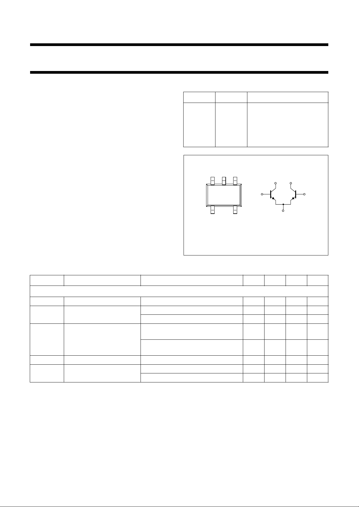
PINNING - SOT353B
SYMBOL PIN DESCRIPTION
b
1
1 base 1
e 2 emitter
b
2
c
2
c
1
handbook, halfpage
4
Top view
3 base 2
4 collector 2
5 collector 1
13
2
b
5
c
c
1
2
1
e
Fig.1 Simplified outline and symbol.
MAM211
b
2
QUICK REFERENCE DATA
SYMBOL PARAMETER CONDITIONS MIN. TYP. MAX. UNIT
Any single transistor
C
re
MSG/G
F noise figure I
h
FE
R
th j-s
feedback capacitance C
maximum power gain IC= 5 mA; VCE= 3 V; f = 900 MHz − 17 − dB
max
BCIe
= 0; VCB= 3 V; f = 1 MHz − 0.25 0.3 pF
= 5 mA; VCE= 3 V; f = 2 GHz − 10 − dB
I
C
= 2 mA; VCE= 3 V; f = 900 MHz;
C
ΓS= Γ
opt
= 3 mA; VCE= 3 V; f = 2 GHz;
I
C
ΓS= Γ
opt
− 1.2 1.7 dB
− 1.9 2.1 dB
DC current gain IC= 5 mA; VCE= 3 V 60 120 250
thermal resistance from
junction to soldering point
single loaded −−230 K/W
double loaded −−115 K/W
1996 Oct 08 2
Philips Semiconductors Product specification
NPN wideband differential transistor BFE505
LIMITING VALUES
In accordance with the Absolute Maximum System (IEC 134).
SYMBOL PARAMETER CONDITIONS MIN. MAX. UNIT
Any single transistor
V
CBO
V
CEO
V
EBO
I
C
P
tot
T
stg
T
j
THERMAL CHARACTERISTICS
SYMBOL PARAMETER CONDITIONS VALUE UNIT
R
th j-s
collector-base voltage open emitter − 20 V
collector-emitter voltage open base − 8V
emitter-base voltage open collector − 2.5 V
DC collector current − 18 mA
total power dissipation up to Ts=118°C; note 1 − 500 mW
storage temperature −65 +175 °C
operating junction temperature − 175 °C
thermal resistance from junction
to soldering point; note 1
single loaded 230 K/W
double loaded 115 K/W
Note to the Limiting values and Thermal characteristics
1. T
is the temperature at the soldering point of the collector pin.
s
1996 Oct 08 3
 Loading...