

Philips BFC520 Datasheet

DISCRETE SEMICONDUCTORS
DATA SH EET
BFC520
NPN wideband cascode transistor
Product specification
Supersedes data of 1996 Oct 08
File under Discrete Semiconductors, SC14
1997 Sep 10
Philips Semiconductors Product specification
NPN wideband cascode transistor BFC520
FEATURES
• Small size
• High power gain at low bias current and high
frequencies
• High reverse isolation
• Low noise figure
• Gold metallization ensures excellent reliability
• Minimum operating voltage V
C2−E1
=1V.
APPLICATIONS
• Low noise, high gain amplifiers
• Oscillator buffer amplifiers
• Wideband voltage-to-current converters.
DESCRIPTION
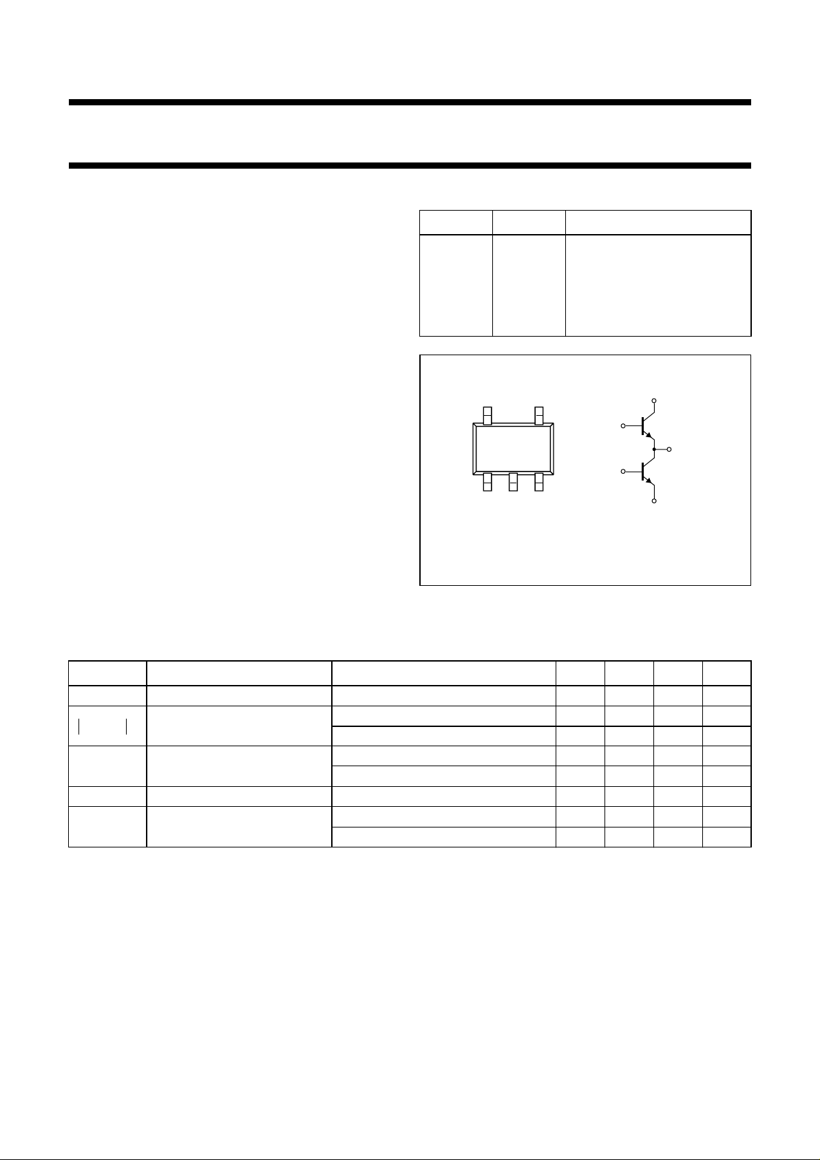
Cascode amplifier with two discrete dies in a surface
mount, 5-pin SOT353 (S-mini) package. The amplifier is
primarily intended for low power RF communications
equipment, such as pagers and cordless phones and has
a very low feedback capacitance resulting in high isolation.
PINNING - SOT353
SYMBOL PIN DESCRIPTION
b
2
e
1
b
1
c
1/e2
c
2
handbook, halfpage
Top view
1 base 2
2 emitter 1
3 base 1
4 collector 1/emitter 2
5 collector 2
5
4
31
2
c
2
b
2
c1/e
b
1
e
1
MAM212
Fig.1 Simplified outline and symbol.
2
QUICK REFERENCE DATA
V
= 3 V; IC= 20 mA; VB2= 2.1 V; b2 connected to ground via 1 nF (0603) capacitor, e1 connected directly to
C2−E1
ground.
SYMBOL PARAMETER CONDITIONS MIN. TYP. MAX. UNIT
C
re
s21s12⁄
MSG maximum stable power gain
F noise figure I
R
th j-s
feedback capacitance C
maximum isolation f = 900 MHz; T
2
B1−C2
f = 2 GHz; T
f = 900 MHz; T
(narrowband)
thermal resistance from
junction to soldering point
f = 2 GHz; T
= 5 mA; f = 900 MHz; ΓS= Γ
C
single loaded −−230 K/W
double loaded −−115 K/W
−−10 fF
=25°C −−63 − dB
amb
=25°C −−38 − dB
amb
=25°C − 31 − dB
amb
=25°C − 19 − dB
amb
opt
− 1.3 1.6 dB
1997 Sep 10 2
Philips Semiconductors Product specification
NPN wideband cascode transistor BFC520
LIMITING VALUES
In accordance with the Absolute Maximum System (IEC 134).
SYMBOL PARAMETER CONDITIONS MIN. MAX. UNIT
Any single transistor
V
CBO
V
CEO
V
EBO
I
C
P
tot
T
stg
T
j
THERMAL CHARACTERISTICS
SYMBOL PARAMETER CONDITIONS VALUE UNIT
R
th j-s
collector-base voltage open emitter − 20 V
collector-emitter voltage open base − 8V
emitter-base voltage open collector − 2.5 V
DC collector current − 70 mA
total power dissipation up to Ts=60°C; note 1 − 1W
storage temperature −65 +175 °C
junction temperature − 175 °C
thermal resistance from junction
to soldering point; note 1
single loaded 230 K/W
double loaded 115 K/W
Note to the Limiting values and Thermal characteristics
is the temperature at the soldering point of the collector pin.
1. T
s
1997 Sep 10 3
Philips Semiconductors Product specification
NPN wideband cascode transistor BFC520
CHARACTERISTICS
Tj=25°C unless otherwise specified.
SYMBOL PARAMETER CONDITIONS MIN. TYP. MAX. UNIT
DC characteristics of any single transistor
V
(BR)CBO
V
(BR)CEO
V
(BR)EBO
I
CBO
h
FE
AC characteristics of the cascode configuration
f
T
C
c
C
re2
C
re
MSG maximum stable power gain; note 1 I
2
s
21
s21s12⁄
F noise figure I
IP
3
collector-base breakdown voltage IC= 2.5 µA; IE=0 20 −−V
collector-emitter breakdown voltage IC=10µA; IB=0 8 −−V
emitter-base breakdown voltage IE= 2.5 µA; IC= 0 2.5 −−V
collector-base leakage current IE= 0; VCB=6V −−50 nA
DC current gain IC= 20 mA; VCE= 6 V 60 120 250
transition frequency IC= 20 mA; V
C2-E1
=3V;
− 7 − GHz
f = 1 GHz
collector capacitance T2 IE=ie= 0; V
C2-B2
=1V;
− 0.55 − pF
f = 1 MHz
feedback capacitance T2 IC= 0; V
feedback capacitance IC= 0; V
= 20 mA; V
C
f = 900 MHz; T
= 20 mA; V
I
C
f = 2 GHz; T
insertion power gain I
= 20 mA; V
C
f = 900 MHz; T
I
= 20 mA; V
C
f = 2 GHz; T
maximum isolation; note 2 f = 900 MHz − 63 − dB
2
=3V;f=1MHz − 500 − fF
C2-E1
=3V;f=1MHz −−10 fF
C2-E1
C2-E1
C2-E1
amb
C2-E1
C2-E1
amb
=3V;
=25°C
amb
=3V;
=25°C
=3V;
=25°C
amb
=3V;
=25°C
− 31 − dB
− 19 − dB
− 17 − dB
− 13 − dB
f = 2 GHz − 38 − dB
= 5 mA; V
C
f = 900 MHz; ΓS= Γ
C2-E1
=3V;
opt
− 1.3 1.6 dB
third order intercept point (input) note 3 −−18 − dBm
Notes
1. MSG =
s12s21⁄ kk21––
×
1s
k
=
-----------------------------------------------------------------------------------------------------------------
2. Maximum isolation is defined as the isolation when S
3. IC=5 mA; VCE= 3 V; RS=50Ω; ZL= opt; T
fp= 900 MHz; fq= 902 MHz; measured at f
11s22
amb
(2p−q)
× s12s21×–
21
=25°C;
= 904 MHz.
1997 Sep 10 4
2s
12s21
2
–+
2
s
11
××
2
s
–
22
of the amplifier is reduced to unity (buffer application).
 Loading...