

Philips BF998R, BF998 Datasheet

DISCRETE SEMICONDUCTORS
DATA SH EET
BF998; BF998R
Silicon N-channel dual-gate
MOS-FETs
Product specification
Supersedes data of April 1991
File under Discrete Semiconductors, SC07
1996 Aug 01
Philips Semiconductors Product specification
Silicon N-channel dual-gate MOS-FETs BF998; BF998R
FEATURES
• Short channel transistor with high forward transfer
admittance to input capacitance ratio
• Low noise gain controlled amplifier up to 1 GHz.
APPLICATIONS
• VHF and UHF applications with 12 V supply voltage,
such as television tuners and professional
communications equipment.
DESCRIPTION
Depletion type field effect transistor in a plastic
microminiature SOT143 or SOT143R package with source
and substrate interconnected. The transistors are
protected against excessive input voltage surges by
integrated back-to-back diodes between gates and
source.
CAUTION
The device is supplied in an antistatic package. The
gate-source input must be protected against static
discharge during transport or handling.
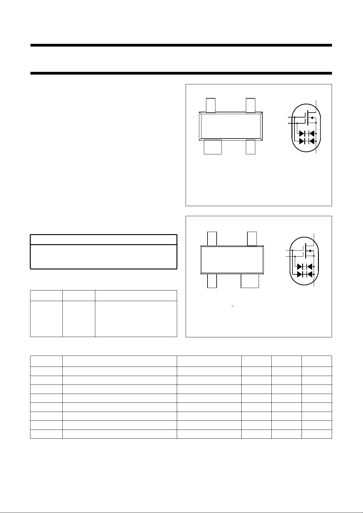
handbook, halfpage
Top view
Marking code: MOp.
Fig.1 Simplified outline (SOT143)
handbook, halfpage
43
21
and symbol; BF998.
34
MAM039
g
g
d
g
2
g
1
s,b
d
2
1
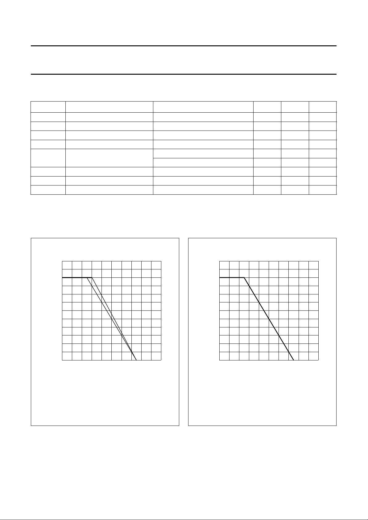
PINNING
PIN SYMBOL DESCRIPTION
1 s, b source
Top view
Marking code: MOp.
12
MAM040
2 d drain
3g
4g
gate 2
2
gate 1
1
Fig.2 Simplified outline (SOT143R)
and symbol; BF998R.
QUICK REFERENCE DATA
SYMBOL PARAMETER CONDITIONS TYP. MAX. UNIT
V
DS
I
D
P
tot
forward transfer admittance 24 − mS
y
fs
C
ig1-s
C
rs
drain-source voltage − 12 V
drain current − 30 mA
total power dissipation − 200 mW
input capacitance at gate 1 2.1 − pF
reverse transfer capacitance f = 1 MHz 25 − fF
F noise figure f = 800 MHz 1 − dB
T
j
operating junction temperature − 150 °C
s,b
1996 Aug 01 2
Philips Semiconductors Product specification
Silicon N-channel dual-gate MOS-FETs BF998; BF998R
LIMITING VALUES
In accordance with the Absolute Maximum Rating System (IEC 134).
SYMBOL PARAMETER CONDITIONS MIN. MAX. UNIT
V
DS
I
D
±I
G1
±I
G2
P
tot
P
tot
T
stg
T
j
Notes
1. Device mounted on a ceramic substrate, 8 mm × 10 mm × 0.7 mm.
2. Device mounted on a printed-circuit board.
drain-source voltage − 12 V
drain current − 30 mA
gate 1 current − 10 mA
gate 2 current − 10 mA
total power dissipation; BF998 up to T
up to T
total power dissipation; BF998R up to T
=60°C; see Fig.3; note 1 − 200 mW
amb
=50°C; see Fig.3; note 2 − 200 mW
amb
=50°C; see Fig.4; note 1 − 200 mW
amb
storage temperature −65 +150 °C
operating junction temperature − 150 °C
handbook, halfpage
200
P
tot max
(mW)
100
0
0 200100
(1) Ceramic substrate.
(2) Printed-circuit board.
(2) (1)
Fig.3 Power derating curves; BF998.
T
amb
o
( C)
MLA198
handbook, halfpage
200
P
tot max
(mW)
100
0
0 200100
Fig.4 Power derating curve; BF998R.
T
amb
MGA002
(°C)
1996 Aug 01 3

Philips Semiconductors Product specification
Silicon N-channel dual-gate MOS-FETs BF998; BF998R
THERMAL CHARACTERISTICS
SYMBOL PARAMETER CONDITIONS VALUE UNIT
R
th j-a
R
th j-a
Notes
1. Device mounted on a ceramic substrate, 8 mm × 10 mm × 0.7 mm.
2. Device mounted on a printed-circuit board.
STATIC CHARACTERISTICS
=25°C; unless otherwise specified.
T
j
SYMBOL PARAMETER CONDITIONS MIN. MAX. UNIT
±V
(BR)G1-SS
±V
(BR)G2-SS
−V
(P)G1-S
−V
(P)G2-S
I
DSS
±I
G1-SS
±I
G2-SS
thermal resistance from junction to ambient in free air; BF998 note 1 460 K/W
note 2 500 K/W
thermal resistance from junction to ambient in free air; BF998R note 1 500 K/W
gate 1-source breakdown voltage V
gate 2-source breakdown voltage V
gate 1-source cut-off voltage V
gate 2-source cut-off voltage V
drain-source current V
gate 1 cut-off current V
gate 2 cut-off current V
G2-S=VDS
G1-S=VDS
G2-S
G1-S
G2-S
G2-S=VDS
G1-S=VDS
= 0; I
= 0; I
= ±10 mA 6 20 V
G1-SS
= ±10 mA 6 20 V
G2-SS
=4V; VDS=8V; ID=20µA − 2.0 V
= 0; VDS=8V; ID=20µA − 1.5 V
=4V; VDS=8V; V
= 0; V
G1-S
= 0; V
G2-S
= 0; note 1 2 18 mA
G1-S
= ±5V − 50 nA
= ±5V − 50 nA
Note
1. Measured under pulse condition.
DYNAMIC CHARACTERISTICS
Common source; T
=25°C; VDS=8V;V
amb
= 4 V; ID= 10 mA.
G2-S
SYMBOL PARAMETER CONDITIONS MIN. TYP. MAX. UNIT
y
forward transfer admittance f = 1 kHz 21 24 − mS
fs
C
ig1-s
C
ig2-s
C
os
C
rs
F noise figure f = 200 MHz; G
input capacitance at gate 1 f = 1 MHz − 2.1 2.5 pF
input capacitance at gate 2 f = 1 MHz − 1.2 − pF
output capacitance f = 1 MHz − 1.05 − pF
reverse transfer capacitance f = 1 MHz − 25 − fF
f = 800 MHz; G
= 2 mS; BS=B
S
= 3.3 mS; BS=B
S
Sopt
− 0.6 − dB
− 1.0 − dB
Sopt
1996 Aug 01 4
 Loading...