

Page 1
DISCRETE SEMICONDUCTORS
DATA SH EET
BF992; BF992R
Silicon N-channel dual-gate
MOS-FETs
Product specification
Supersedes data of April 1991
File under Discrete Semiconductors, SC07
1996 Jul 30
Page 2
Philips Semiconductors Product specification
Silicon N-channel dual-gate MOS-FETs BF992; BF992R
APPLICATIONS
• VHF applications such as VHF television tuners and FM
tuners with 12 V supply voltage. The device is also
suitable for use in professional communications
equipment.
DESCRIPTION
Depletion type field-effect transistor in a plastic
micro-miniature SOT143 or SOT143R package with
source and substrate interconnected.
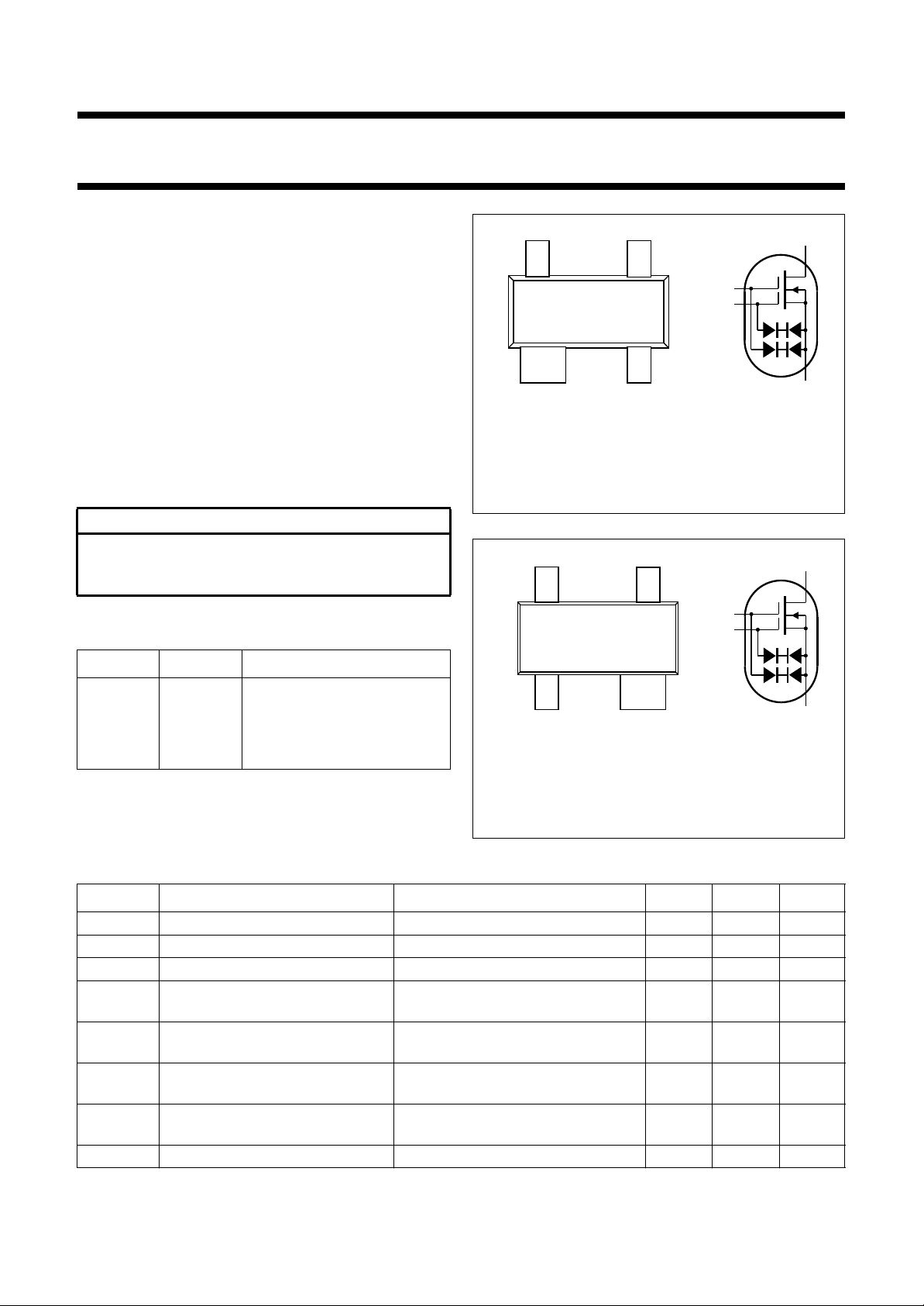
handbook, halfpage
Top view
43
21
MAM039
g
2
g
1
d
s,b
The transistors are protected against excessive input
voltage surges by integrated back-to-back diodes between
gates and source.
CAUTION
The device is supplied in an antistatic package. The
gate-source input must be protected against static
discharge during transport or handling.
PINNING
PIN SYMBOL DESCRIPTION
1 s,b source
2 d drain
3g
4g
gate 2
2
gate 1
1
QUICK REFERENCE DATA
Marking code: M92.
Fig.1 Simplified outline (SOT143) and
symbol; BF992.
handbook, halfpage
Marking code: M52.
34
Top view
g
g
12
MAM040
Fig.2 Simplified outline (SOT143R) and
symbol; BF992R.
d
2
1
s,b
SYMBOL PARAMETER CONDITIONS TYP. MAX. UNIT
V
DS
I
D
P
tot
forward transfer admittance f = 1 kHz; ID= 15 mA; VDS=10V;
Y
fs
C
ig1-s
C
rs
F noise figure G
T
j
drain-source voltage (DC) − 20 V
drain current (DC) − 40 mA
total power dissipation T
=60°C − 200 mW
amb
25 − mS
V
=4V
G2-S
input capacitance at gate 1 f = 1 MHz; ID= 15 mA; VDS=10V;
V
=4V
G2-S
reverse transfer capacitance f = 1 MHz; ID= 15 mA; VDS=10V;
V
=4V
G2-S
= 2 mS; ID= 15 mA; VDS=10V;
S
V
= 4 V; f = 200 MHz
G2-S
4 − pF
30 − fF
1.2 − dB
operating junction temperature − 150 °C
1996 Jul 30 2
Page 3
Philips Semiconductors Product specification
Silicon N-channel dual-gate MOS-FETs BF992; BF992R
LIMITING VALUES
In accordance with the Absolute Maximum Rating System (IEC 134).
SYMBOL PARAMETER CONDITIONS MIN. MAX. UNIT
V
DS
I
D
±I
G1
±I
G2
P
tot
T
stg
T
j
Note
1. Device mounted on a ceramic substrate, 8 mm × 10 mm × 0.7 mm.
drain-source voltage − 20 V
drain current − 40 mA
gate 1 current − 10 mA
gate 2 current − 10 mA
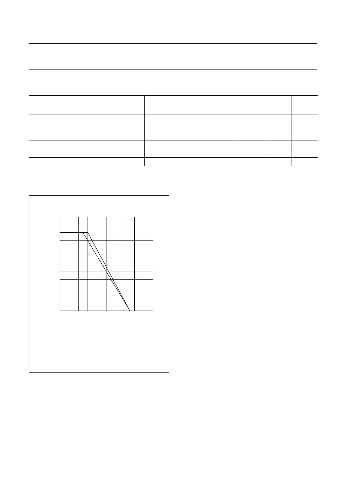
total power dissipation up to T
=60°C; see Fig.3; note 1 − 200 mW
amb
storage temperature −65 +150 °C
operating junction temperature − 150 °C
handbook, halfpage
200
P
tot max
(mW)
100
0
0 200100
(1) BF992.
(2) BF992R.
Fig.3 Power derating curves.
(2) (1)
T
amb
o
( C)
MLA198
1996 Jul 30 3
Page 4

Philips Semiconductors Product specification
Silicon N-channel dual-gate MOS-FETs BF992; BF992R
THERMAL CHARACTERISTICS
SYMBOL PARAMETER CONDITIONS VALUE UNIT
R
th j-a
Note
1. Device mounted on a ceramic substrate, 8 mm × 10 mm × 0.7 mm.
STATIC CHARACTERISTICS
=25°C; unless otherwise specified.
T
j
SYMBOL PARAMETER CONDITIONS MIN. MAX. UNIT
±V
(BR)G1-SS
±V
(BR)G2-SS
−V
(P)G1-S
−V
(P)G2-S
±I
G1-SS
±I
G2-SS
thermal resistance from junction to ambient in free air note 1
BF992 460 K/W
BF992R 500 K/W
gate 1-source breakdown voltage V
gate 2-source breakdown voltage V
gate 1-source cut-off voltage V
gate 2-source cut-off voltage V
gate 1 cut-off current V
gate 2 cut-off current V
G2-S=VDS
G1-S=VDS
G2-S
G1-S
G2-S=VDS
G1-S=VDS
= 0; I
= 0; I
= ±10 mA 8 20 V
G1-SS
= ±10 mA 8 20 V
G2-SS
=4V; VDS=10V; ID=20µA 0.2 1.3 V
= 0; VDS= 10 V; ID=20µA 0.2 1.1 V
= 0; V
= 0; V
= ±7V − 25 nA
G1-S
= ±7V − 25 nA
G2-S
DYNAMIC CHARACTERISTICS
Common source; T
=25°C; VDS=10V;V
amb
= 4 V; ID= 15 mA; unless otherwise specified.
G2-S
SYMBOL PARAMETER CONDITIONS MIN. TYP. MAX. UNIT
y
forward transfer admittance 20 25 − mS
fs
C
ig1-s
C
ig2-s
C
os
C
rs
F noise figure f = 200 MHz; G
input capacitance at gate 1 f = 1 MHz − 4 − pF
input capacitance at gate 2 f = 1 MHz − 1.7 − pF
output capacitance f = 1 MHz − 2 − pF
reverse transfer capacitance f = 1 MHz − 30 40 fF
=2mS − 1.2 − dB
S
1996 Jul 30 4
Page 5

Philips Semiconductors Product specification
Silicon N-channel dual-gate MOS-FETs BF992; BF992R
24
handbook, halfpage
ID
(mA)
20
16
12
8
4
0
V
= 4V; Tj=25°C.
G2-S
2468
010
V
Fig.4 Output characteristics; typical values.
G1-S
VDS (V)
MGE797
= 0.2 V
0.1 V
0 V
−0.1 V
−0.2 V
−0.3 V
−0.4 V
−0.5 V
−0.6 V
30
handbook, halfpage
ID
(mA)
20
10
0
12
−11
VDS= 10 V; Tj=25°C.
V
G2-S
= 5 V
0
V
G1-S
4 V
MGE799
3 V
2 V
1 V
0 V
(V)
Fig.5 Transfer characteristics; typical values.
30
handbook, halfpage
|yfs|
(mS)
20
10
0
020
VDS= 10 V; Tj=25°C.
V
G2-S
= 0 V
10
ID (mA)
MGE798
1 V
Fig.6 Forward transfer admittance as a function
of drain current; typical values.
5 V
4 V
3 V
2 V
30
handbook, halfpage
Yfs
(mS)
20
10
0
−11
VDS= 10 V; Tj=25°C.
0
V
G1-S
MGE800
V
(V)
Fig.7 Forward transfer admittance as a function
of gate 1-source voltage; typical values.
G2-S
=
5 V
4 V
3 V
2 V
1 V
0 V
1996 Jul 30 5
Page 6

Philips Semiconductors Product specification
Silicon N-channel dual-gate MOS-FETs BF992; BF992R
2
10
handbook, halfpage
yis
MGE794
(mS)
10
bis
1
gis
−1
10
−2
10
10
VDS= 10 V; V
= 4 V; ID= 15 mA; T
G2-S
2
10
amb
f (MHz)
=25°C.
10
Fig.8 Input admittance as a function of frequency;
typical values.
10
handbook, halfpage
MGE793
yos
(mS)
bos
1
2
amb
gos
f (MHz)
=25°C.
3
10
−1
10
−2
3
10
10 10
VDS= 10 V; V
= 4 V; ID= 15 mA; T
G2-S
Fig.9 Output admittance as a function of
frequency; typical values.
25
handbook, halfpage
Yfs
(mS)
MGE795
gfs
20
15
10
−bfs
5
0
10 10
VDS= 10 V; V
G2-S
= 4 V; ID= 15 mA; T
2
amb
f (MHz)
=25°C.
Fig.10 Forward transfer admittance as a function
of frequency; typical values.
120
handbook, halfpage
MGE796
yrs
(µS)
80
−brs
40
grs
3
10
0
10 10
VDS= 10 V; V
= 4 V; ID= 15 mA; T
G2-S
2
amb
f (MHz)
=25°C.
3
10
Fig.11 Reverse transfer admittance as a function
of frequency; typical values.
1996 Jul 30 6
Page 7

Philips Semiconductors Product specification
Silicon N-channel dual-gate MOS-FETs BF992; BF992R
PACKAGE OUTLINES
handbook, full pagewidth
Dimensions in mm.
10
max
3.0
0.150
1.1
30
max
0.090
0.1
max
max
o
o
10
0.88
0.75
0.60
o
max
2.8
1.9
43
1
2
0
0.1
TOP VIEW
0.48
1.7
0
0.1
B
A
1.4
1.2
M0.1 AB
2.5
max
0.2
MBC845
M
AB
Fig.12 SOT143.
handbook, full pagewidth
Dimensions in mm.
0.40
0.25
10
max
o
max
1.1
30
max
0.150
0.090
0.1
max
max
o
o
10
0.48
0.38
Fig.13 SOT143R.
1996 Jul 30 7
3.0
2.8
1.9
34
2
1
0.88
0.78
1.7
M0.1 B
TOP VIEW
B
A
1.4
1.2
MBC844
2.5
max
0.2
A
M
Page 8

Philips Semiconductors Product specification
Silicon N-channel dual-gate MOS-FETs BF992; BF992R
DEFINITIONS
Data Sheet Status
Objective specification This data sheet contains target or goal specifications for product development.
Preliminary specification This data sheet contains preliminary data; supplementary data may be published later.
Product specification This data sheet contains final product specifications.
Limiting values
Limiting values given are in accordance with the Absolute Maximum Rating System (IEC 134). Stress above one or
more of the limiting values may cause permanent damage to the device. These are stress ratings only and operation
of the device at these or at any other conditions above those given in the Characteristics sections of the specification
is not implied. Exposure to limiting values for extended periods may affect device reliability.
Application information
Where application information is given, it is advisory and does not form part of the specification.
LIFE SUPPORT APPLICATIONS
These products are not designed for use in life support appliances, devices, or systems where malfunction of these
products can reasonably be expected to result in personal injury. Philips customers using or selling these products for
use in such applications do so at their own risk and agree to fully indemnify Philips for any damages resulting from such
improper use or sale.
1996 Jul 30 8
 Loading...