

Philips BF904AWR Datasheet

DISCRETE SEMICONDUCTORS
DATA SH EET
BF904A; BF904AR; BF904AWR
N-channel dual gate MOS-FETs
Product specification
Supersedes data of 1999 Feb 01
1999 May 14

Philips Semiconductors Product specification
N-channel dual gate MOS-FETs BF904A; BF904AR; BF904AWR
FEATURES
• Specially designed for use at 5 V
supply voltage
• Short channel transistor with high
transfer admittance to input
capacitance ratio
• Low noise gain controlled amplifier
up to 1 GHz
• Superior cross-modulation
performance during AGC.
APPLICATIONS
• VHF and UHF applications with
3 to 7 V supply voltage such as
television tuners and professional
communications equipment.
DESCRIPTION
Enhancement type field-effect
transistors. The transistors consist of
an amplifier MOS-FET with source
and substrate interconnected and an
internal bias circuit to ensure good
cross-modulation performance during
AGC.
The BF904A, BF904AR and
BF904AWR are encapsulated in the
SOT143B, SOT143R and SOT343R
plastic packages respectively.
PINNING
PIN DESCRIPTION
1 source
2 drain
3 gate 2
4 gate 1
handbook, 2 columns
Top view
BF904AR marking code: M42.
Fig.2 Simplified outline
(SOT143R).
43
12
MSB035
handbook, 2 columns
12
Top view
BF904A marking code: M41.
Fig.1 Simplified outline
(SOT143B).
alfpage
21
Top view
BF904AWR marking code: MH.
Fig.3 Simplified outline
(SOT343R).
34
MSB014
43
MSB842
QUICK REFERENCE DATA
SYMBOL PARAMETER CONDITIONS MIN. TYP. MAX. UNIT
V
DS
I
D
P
tot
y
forward transfer admittance 22 25 30 mS
fs
C
ig1-ss
C
rss
drain-source voltage −−7V
drain current −−30 mA
total power dissipation Ts≤ 110 °C −−200 mW
input capacitance at gate 1 − 2.2 2.6 pF
reverse transfer capacitance f = 1 MHz − 25 35 fF
F noise figure f = 800 MHz − 2 − dB
T
j
operating junction temperature −−150 °C
CAUTION
This product is supplied in anti-static packing to prevent damage caused by electrostatic discharge during transport
and handling. For further information, refer to Philips specs.: SNW-EQ-608, SNW-FQ-302A and SNW-FQ-302B.
1999 May 14 2

Philips Semiconductors Product specification
N-channel dual gate MOS-FETs BF904A; BF904AR; BF904AWR
LIMITING VALUES
In accordance with the Absolute Maximum Rating System (IEC 134).
SYMBOL PARAMETER CONDITIONS MIN. MAX. UNIT
V
DS
I
D
I
G1
I
G2
P
tot
T
stg
T
j
Note
1. T
is the temperature of the soldering point of the source lead.
s
drain-source voltage − 7V
drain current − 30 mA
gate 1 current −±10 mA
gate 2 current −±10 mA
total power dissipation Ts≤ 110 °C; note 1; see Fig.4 − 200 mW
storage temperature −65 +150 °C
operating junction temperature − 150 °C
250
handbook, halfpage
P
tot
(mW)
200
150
100
50
0
0 50 100 200
MGL615
150
Ts (°C)
Fig.4 Power derating curve.
1999 May 14 3

Philips Semiconductors Product specification
N-channel dual gate MOS-FETs BF904A; BF904AR; BF904AWR
THERMAL CHARACTERISTICS
SYMBOL PARAMETER CONDITIONS VALUE UNIT
R
th j-s
Note
1. Soldering point of the source lead.
STATIC CHARACTERISTICS
=25°C unless otherwise specified.
T
j
SYMBOL PARAMETER CONDITIONS MIN. MAX. UNIT
V
(BR)G1-SS
V
(BR)G2-SS
V
(F)S-G1
V
(F)S-G2
V
G1-S(th)
V
G2-S(th)
I
DSX
I
G1-SS
I
G2-SS
thermal resistance from junction to soldering point note 1 200 K/W
gate 1-source breakdown voltage V
gate 2-source breakdown voltage V
forward source-gate 1 voltage V
forward source-gate 2 voltage V
gate 1-source threshold voltage V
gate 2-source threshold voltage V
drain-source current V
G2-S=VDS
G1-S=VDS
G2-S=VDS
G1-S=VDS
G2-S
G1-S=VDS
G2-S
= 0; I
= 0; I
= 0; I
= 0; I
= 10 mA 6 15 V
G1-S
= 10 mA 6 15 V
G2-S
= 10 mA 0.5 1.5 V
S-G1
= 10 mA 0.5 1.5 V
S-G2
=4V; VDS=5V; ID=20µA 0.3 1 V
=5V; ID=20µA 0.3 1.2 V
=4V; VDS=5V;
813mA
RG1= 120 kΩ; note 1
gate 1 cut-off current V
gate 2 cut-off current V
G2-S=VDS
G1-S=VDS
= 0; V
= 0; V
=5V − 50 nA
G1-S
=5V − 50 nA
G2-S
Note
1. R
connects gate 1 to VGG= 5 V; see Fig.21.
G1
DYNAMIC CHARACTERISTICS
Common source; T
=25°C; VDS= 5 V; V
amb
= 4 V; ID= 10 mA; unless otherwise specified.
G2-S
SYMBOL PARAMETER CONDITIONS MIN. TYP. MAX. UNIT
y
forward transfer admittance pulsed; Tj=25°C 222530mS
fs
C
ig1-s
C
ig2-s
C
os
C
rs
F noise figure f = 200 MHz; G
input capacitance at gate 1 f = 1 MHz − 2.2 2.6 pF
input capacitance at gate 2 f = 1 MHz 1 1.5 2 pF
drain-source capacitance f = 1 MHz 1 1.4 1.7 pF
reverse transfer capacitance f = 1 MHz − 25 35 fF
f = 800 MHz; G
= 2 mS; BS=B
S
S=GSopt
; BS=B
− 1 1.5 dB
Sopt
− 2 2.8 dB
Sopt
1999 May 14 4
Philips Semiconductors Product specification
N-channel dual gate MOS-FETs BF904A; BF904AR; BF904AWR
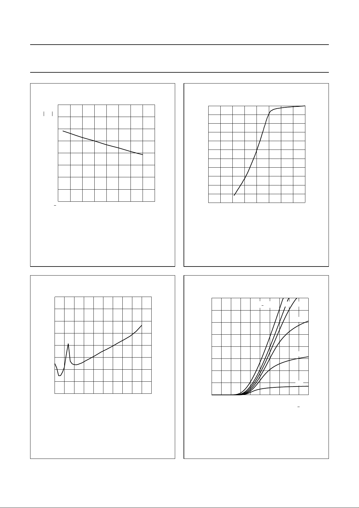
100
MLD268
o
T ( C)
j
40
Y
fs
(mS)
30
20
10
0
50 0 50 150
Fig.5 Transfer admittance as a function of the
junction temperature; typical values.
handbook, halfpage
reduction
0
gain
(dB)
10
20
30
40
50
01234
f =50 MHz.
Fig.6 Typical gain reduction as a function of
the AGC voltage; see Fig.21.
MRA769
V (V)
AGC
120
handbook, halfpage
V
unw
(dB V)
µ
110
100
90
80
0 1020304050
VDS= 5V; VGG= 5V; fw= 50MHz.
f
= 60MHz; T
unw
=25°C; RG1= 120kΩ.
amb
gain reduction (dB)
MRA771
Fig.7 Unwanted voltage for 1% cross-modulation
as a function of gain reduction; typical
values; see Fig.21.
20
I
D
(mA)
15
10
VDS=5V.
Tj=25°C.
5
0
0
0.4 2.0
V = 4 V
G2 S
0.8 1.2 1.6
3 V 2.5 V
V (V)
G1 S
Fig.8 Transfer characteristics; typical values.
MLD270
2 V
1.5 V
1 V
1999 May 14 5
 Loading...