

Page 1
DISCRETE SEMICONDUCTORS
DATA SH EET
M3D067
BF870; BF872
PNP high-voltage transistors
Product specification
Supersedes data of September 1994
File under Discrete Semiconductors, SC04
1996 Dec 09
Page 2
Philips Semiconductors Product specification
PNP high-voltage transistors BF870; BF872
FEATURES
• Low feedback capacitance.
handbook, halfpage
APPLICATIONS
• For use in class-B video output stages of colour
television receivers.
2
DESCRIPTION
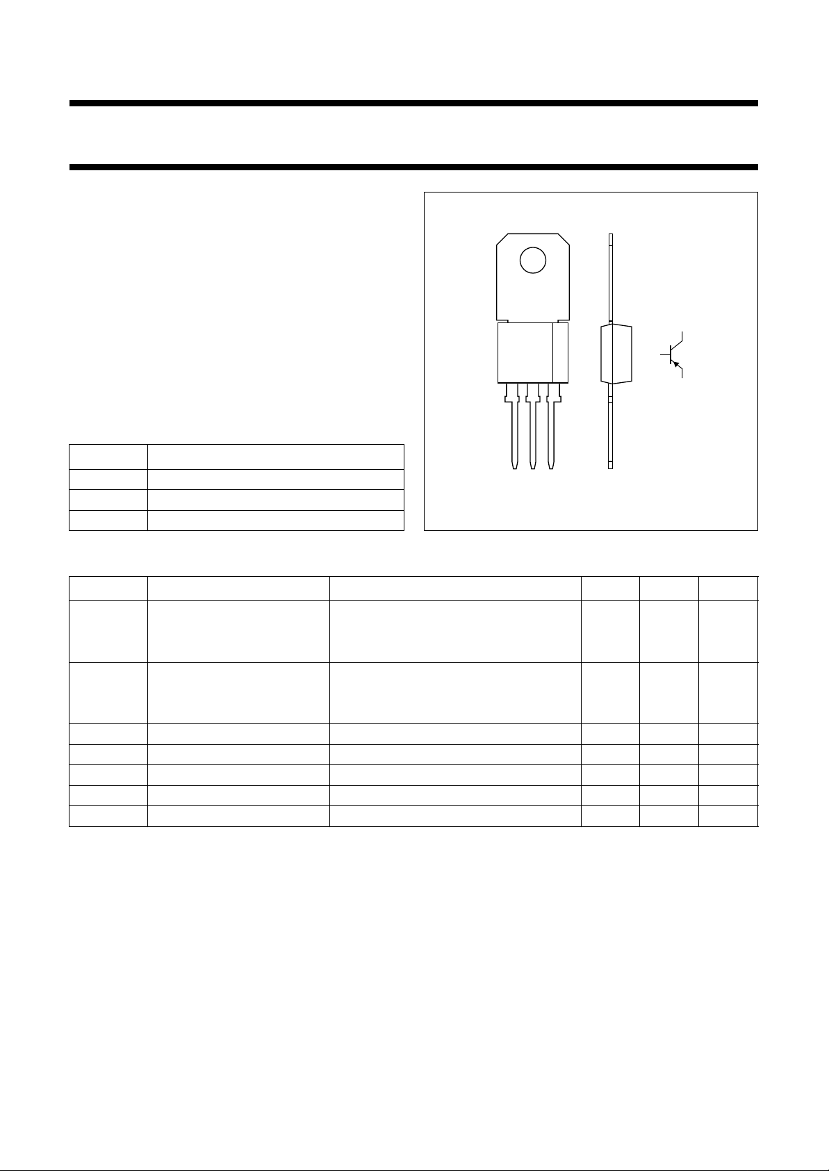
PNP transistors in a TO-202 plastic package.
NPN complements: BF869 and BF871.
PINNING
PIN DESCRIPTION
1 emitter
2 collector, connected to mounting base
3 base
123
Fig.1 Simplified outline (TO-202) and symbol.
3
1
MBH792
QUICK REFERENCE DATA
SYMBOL PARAMETER CONDITIONS MIN. MAX. UNIT
V
CBO
collector-base voltage open emitter
BF870 −−250 V
BF872 −−300 V
V
CEO
collector-emitter voltage open base
BF870 −−250 V
BF872 −−300 V
I
CM
P
tot
h
FE
C
re
f
T
peak collector current −−100 mA
total power dissipation Tmb≤ 25 °C − 5W
DC current gain IC= −25 mA; VCE= −20 V; Tj=25°C50 −
feedback capacitance IC=ic= 0; VCE= −30 V; f = 1MHz − 2.2 pF
transition frequency IC= −10 mA; VCE= −10 V; f = 100 MHz 60 − MHz
1996 Dec 09 2
Page 3
Philips Semiconductors Product specification
PNP high-voltage transistors BF870; BF872
LIMITING VALUES
In accordance with the Absolute Maximum Rating System (IEC 134).
SYMBOL PARAMETER CONDITIONS MIN. MAX. UNIT
V
CBO
V
CEO
V
EBO
I
C
I
CM
I
BM
P
tot
T
stg
T
j
T
amb
collector-base voltage open emitter
BF870 −−250 V
BF872 −−300 V
collector-emitter voltage open base
BF870 −−250 V
BF872 −−300 V
emitter-base voltage open collector −−5V
collector current (DC) −−50 nA
peak collector current −−100 mA
peak base current −−50 mA
total power dissipation T
≤ 25 °C − 1.6 W
amb
≤ 25 °C − 5W
T
mb
storage temperature −65 +150 °C
junction temperature − 150 °C
operating ambient temperature −65 +150 °C
THERMAL CHARACTERISTICS
SYMBOL PARAMETER VALUE UNIT
R
R
th j-a
th j-mb
thermal resistance from junction to ambient 78 K/W
thermal resistance from junction to mounting base 25 K/W
CHARACTERISTICS
T
=25°C unless otherwise specified.
j
SYMBOL PARAMETER CONDITIONS MIN. MAX. UNIT
I
CBO
I
EBO
h
FE
V
C
f
T
CEsat
re
collector cut-off current IE= 0; VCB= −200 V −−10 nA
= 0; VCB= −200 V; Tj= 150 °C −−10 µA
I
E
emitter cut-off current IC= 0; VEB= −5V −−50 nA
DC current gain IC= −25 mA; VCE= −20 V 50 −
collector-emitter saturation voltage IC= −30 mA; IB= −5mA −−600 mV
feedback capacitance IC=ic= 0; VCE= −30 V; f = 1MHz − 2.2 pF
transition frequency IC= −10 mA; VCE= −10 V; f = 100 MHz 60 − MHz
1996 Dec 09 3
Page 4

Philips Semiconductors Product specification
PNP high-voltage transistors BF870; BF872
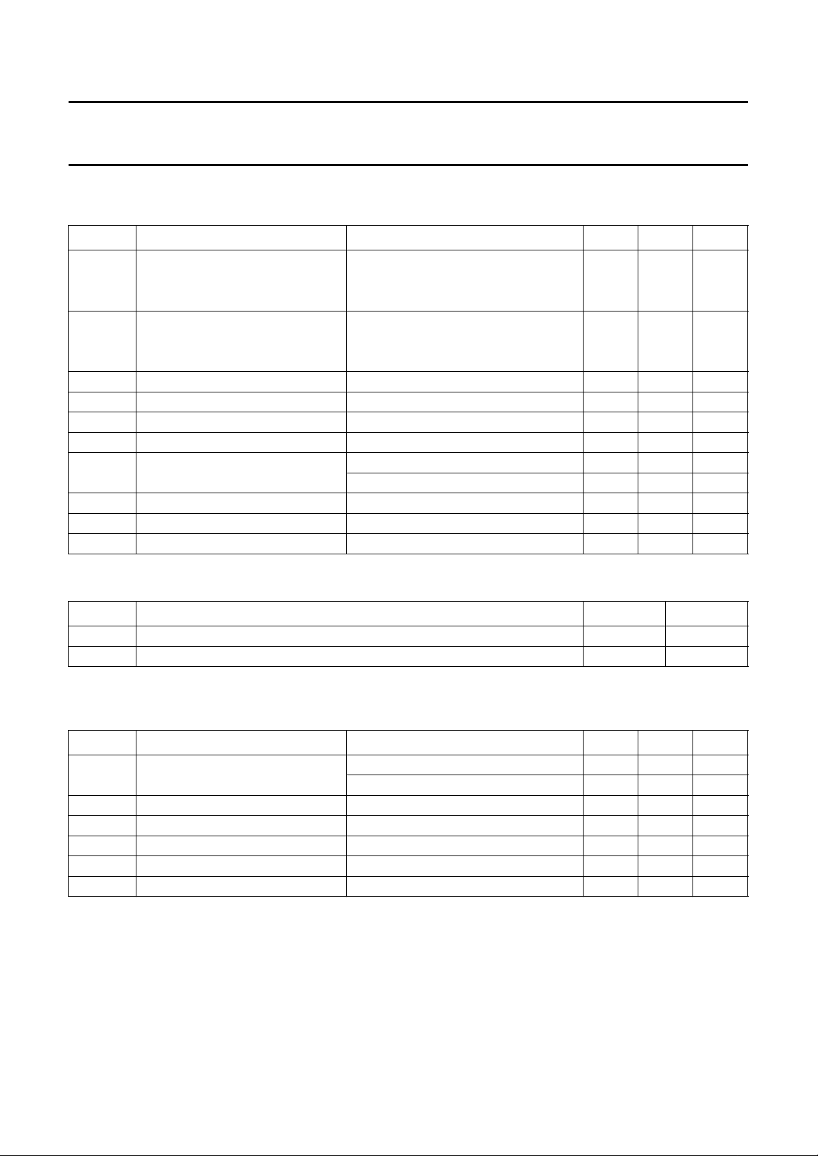
PACKAGE OUTLINE
handbook, full pagewidth
2.5 max
(1)
123
10.4 max
3.8
3.6
2.542.54
3.8
2.4 max
0.8
(3x)
0.6
4.6
max
24.2
max
0.56 max
0.65 max
1.6
8.6
max
12.2
min
10
Dimensions in mm.
(1) Terminal dimensions within this zone are uncontrolled.
Fig.2 TO-202.
1996 Dec 09 4
MGA322
Page 5

Philips Semiconductors Product specification
PNP high-voltage transistors BF870; BF872
DEFINITIONS
Data sheet status
Objective specification This data sheet contains target or goal specifications for product development.
Preliminary specification This data sheet contains preliminary data; supplementary data may be published later.
Product specification This data sheet contains final product specifications.
Limiting values
Limiting values given are in accordance with the Absolute Maximum Rating System (IEC 134). Stress above one or
more of the limiting values may cause permanent damage to the device. These are stress ratings only and operation
of the device at these or at any other conditions above those given in the Characteristics sections of the specification
is not implied. Exposure to limiting values for extended periods may affect device reliability.
Application information
Where application information is given, it is advisory and does not form part of the specification.
LIFE SUPPORT APPLICATIONS
These products are not designed for use in life support appliances, devices, or systems where malfunction of these
products can reasonably be expected to result in personal injury. Philips customers using or selling these products for
use in such applications do so at their own risk and agree to fully indemnify Philips for any damages resulting from such
improper use or sale.
1996 Dec 09 5
Page 6

Philips Semiconductors Product specification
PNP high-voltage transistors BF870; BF872
NOTES
1996 Dec 09 6
Page 7

Philips Semiconductors Product specification
PNP high-voltage transistors BF870; BF872
NOTES
1996 Dec 09 7
Page 8

Philips Semiconductors – a worldwide company
Argentina: see South America
Australia: 34 Waterloo Road, NORTH RYDE, NSW 2113,
Tel. +61 2 9805 4455, Fax. +61 29805 4466
Austria: Computerstr. 6, A-1101 WIEN, P.O. Box 213,
Tel. +43 1 60 101, Fax. +43 1 60 101 1210
Belarus: Hotel Minsk Business Center, Bld. 3, r. 1211, Volodarski Str.6,
220050 MINSK, Tel. +375 172 200 733, Fax. +375 172 200773
Belgium: see The Netherlands
Brazil: seeSouth America
Bulgaria: Philips Bulgaria Ltd., Energoproject, 15thfloor,
51 James Bourchier Blvd., 1407 SOFIA,
Tel. +359 2 689 211, Fax. +359 2689 102
Canada: PHILIPS SEMICONDUCTORS/COMPONENTS,
Tel. +1 800 234 7381
China/Hong Kong: 501 Hong Kong Industrial Technology Centre,
72 Tat Chee Avenue, Kowloon Tong, HONG KONG,
Tel. +852 2319 7888, Fax. +8522319 7700
Colombia: see South America
Czech Republic: see Austria
Denmark: Prags Boulevard 80, PB 1919, DK-2300 COPENHAGEN S,
Tel. +45 32 88 2636, Fax. +45 31 57 1949
Finland: Sinikalliontie 3, FIN-02630 ESPOO,
Tel. +358 9 615800, Fax. +358 9 61580/xxx
France: 4 Rue du Port-aux-Vins, BP317, 92156 SURESNES Cedex,
Tel. +33 1 40 99 6161, Fax. +33 1 4099 6427
Germany: Hammerbrookstraße 69, D-20097 HAMBURG,
Tel. +49 40 23 53 60, Fax. +4940 23536 300
Greece: No. 15, 25th March Street, GR 17778 TAVROS/ATHENS,
Tel. +30 1 4894 339/239, Fax. +30 14814 240
Hungary: seeAustria
India: Philips INDIA Ltd, Shivsagar Estate, A Block, Dr. Annie Besant Rd.
Worli, MUMBAI 400 018, Tel. +91 22 4938541, Fax.+91 224938 722
Indonesia: see Singapore
Ireland: Newstead, Clonskeagh, DUBLIN 14,
Tel. +353 1 7640 000, Fax.+353 17640 200
Israel: RAPAC Electronics, 7 Kehilat Saloniki St, TEL AVIV 61180,
Tel. +972 3 645 0444, Fax.+972 3649 1007
Italy: PHILIPS SEMICONDUCTORS, Piazza IV Novembre 3,
20124 MILANO, Tel. +39 2 6752 2531, Fax. +392 67522557
Japan: Philips Bldg 13-37, Kohnan 2-chome, Minato-ku, TOKYO 108,
Tel. +81 3 3740 5130, Fax. +81 33740 5077
Korea: Philips House, 260-199 Itaewon-dong, Yongsan-ku, SEOUL,
Tel. +82 2 709 1412, Fax. +82 2 709 1415
Malaysia: No. 76 Jalan Universiti, 46200 PETALING JAYA, SELANGOR,
Tel. +60 3 750 5214, Fax. +603 7574880
Mexico: 5900 Gateway East, Suite 200, EL PASO, TEXAS 79905,
Tel. +9-5 800 234 7381
Middle East: see Italy
Netherlands: Postbus 90050, 5600PB EINDHOVEN, Bldg. VB,
Tel. +31 40 27 82785, Fax.+31 4027 88399
New Zealand: 2 Wagener Place, C.P.O. Box 1041, AUCKLAND,
Tel. +64 9 849 4160, Fax. +64 9 849 7811
Norway: Box 1, Manglerud 0612, OSLO,
Tel. +47 22 74 8000, Fax. +47 22 74 8341
Philippines: Philips Semiconductors Philippines Inc.,
106 Valero St. Salcedo Village, P.O. Box2108 MCC,MAKATI,
Metro MANILA, Tel. +63 2 816 6380, Fax. +632 817 3474
Poland: Ul. Lukiska 10, PL 04-123 WARSZAWA,
Tel. +48 22 612 2831, Fax.+48 22612 2327
Portugal: see Spain
Romania: see Italy
Russia: Philips Russia, Ul. Usatcheva 35A, 119048 MOSCOW,
Tel. +7 095 247 9145, Fax.+7 095247 9144
Singapore: Lorong 1, Toa Payoh, SINGAPORE 1231,
Tel. +65 350 2538, Fax. +65 251 6500
Slovakia: see Austria
Slovenia: see Italy
South Africa: S.A. PHILIPS Pty Ltd., 195-215 Main Road Martindale,
2092 JOHANNESBURG, P.O. Box 7430 Johannesburg 2000,
Tel. +27 11 470 5911, Fax.+27 11470 5494
South America: Rua do Rocio 220, 5th floor, Suite 51,
04552-903 São Paulo, SÃO PAULO - SP, Brazil,
Tel. +55 11 821 2333, Fax.+55 11829 1849
Spain: Balmes 22, 08007 BARCELONA,
Tel. +34 3 301 6312, Fax. +34 3 301 4107
Sweden: Kottbygatan 7, Akalla, S-16485 STOCKHOLM,
Tel. +46 8 632 2000, Fax. +46 8 632 2745
Switzerland: Allmendstrasse 140, CH-8027 ZÜRICH,
Tel. +41 1 488 2686, Fax. +41 1 481 7730
Taiwan: PHILIPS TAIWAN Ltd., 23-30F, 66,
Chung Hsiao West Road, Sec. 1, P.O. Box 22978,
TAIPEI 100, Tel. +886 2 382 4443, Fax.+886 2382 4444
Thailand: PHILIPS ELECTRONICS (THAILAND) Ltd.,
209/2 Sanpavuth-Bangna Road Prakanong, BANGKOK 10260,
Tel. +66 2 745 4090, Fax. +66 2 398 0793
Turkey: Talatpasa Cad. No. 5, 80640 GÜLTEPE/ISTANBUL,
Tel. +90 212 279 2770, Fax. +90 212 282 6707
Ukraine: PHILIPS UKRAINE, 4 Patrice Lumumba str., Building B, Floor 7,
252042 KIEV, Tel. +380 44 264 2776, Fax. +38044 2680461
United Kingdom: Philips Semiconductors Ltd., 276 Bath Road, Hayes,
MIDDLESEX UB3 5BX, Tel. +44 181 730 5000, Fax.+44 181754 8421
United States: 811 East Arques Avenue, SUNNYVALE, CA 94088-3409,
Tel. +1 800 234 7381
Uruguay: see South America
Vietnam: see Singapore
Yugoslavia: PHILIPS, Trg N. Pasica 5/v, 11000 BEOGRAD,
Tel. +381 11 625 344, Fax.+38111 635777
For all other countries apply to: Philips Semiconductors, Marketing & Sales Communications,
Building BE-p, P.O. Box 218, 5600 MD EINDHOVEN, TheNetherlands, Fax.+31 4027 24825
© Philips Electronics N.V. 1996 SCA52
All rights are reserved. Reproduction in whole or in part is prohibited without the prior written consent of the copyright owner.
The information presented in this document does not form part of any quotation or contract, is believed to be accurate and reliable and may be changed
without notice. No liability will be accepted by the publisher for any consequence of its use. Publication thereof does not convey nor imply any license
under patent- or other industrial or intellectual property rights.
Internet: http://www.semiconductors.philips.com
Printed in The Netherlands 117041/00/02/pp8 Date of release: 1996Dec 09 Document order number: 9397 75001573
 Loading...