

Page 1
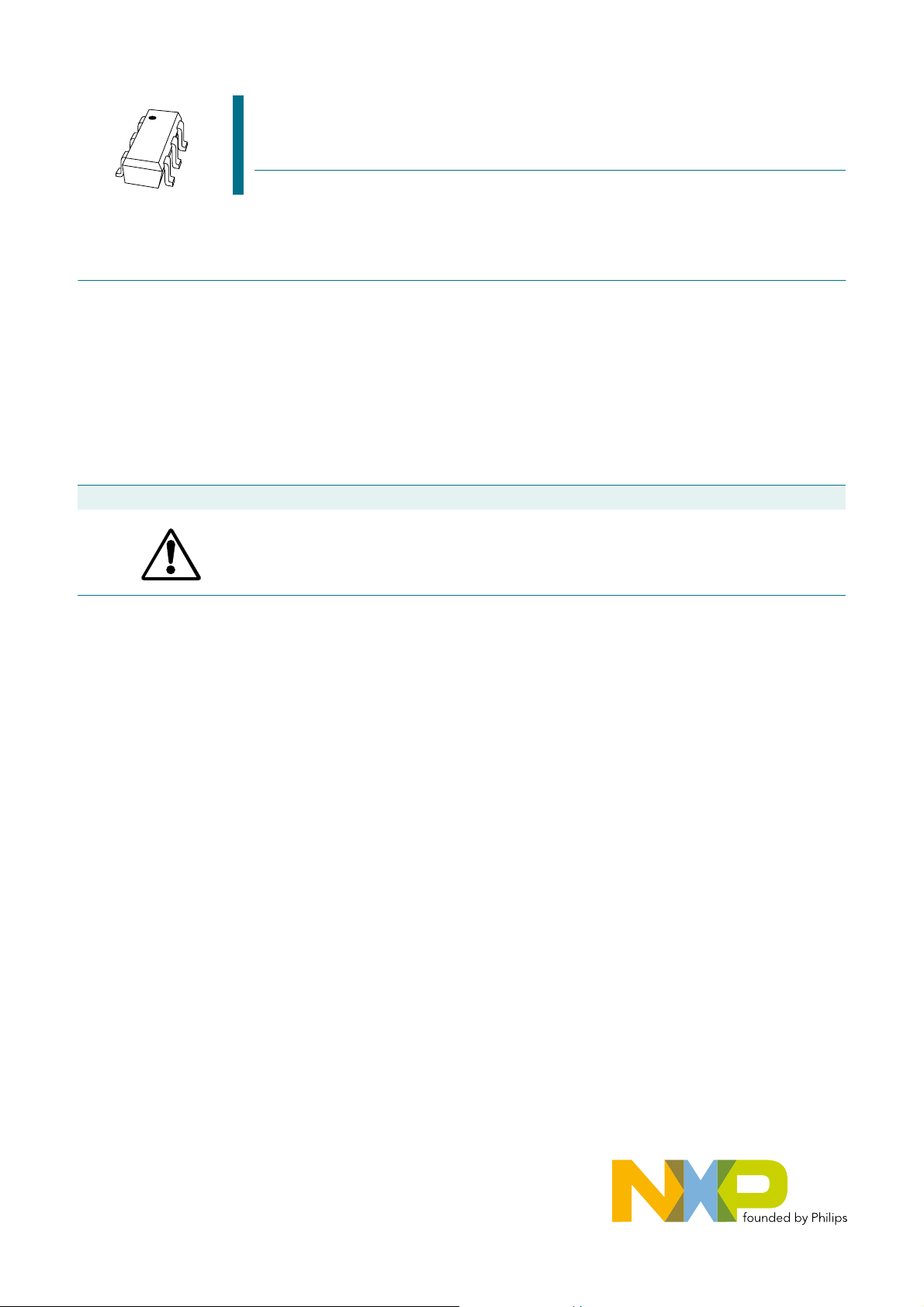
BF1210
Dual N-channel dual gate MOSFET
Rev. 01 — 25 October 2006 Product data sheet
1. Product profile
1.1 General description
The BF1210 is a combination of two dual gate MOSFET amplifiers with shared source
and gate2 leads.
The source and substrate are interconnected. Internal bias circuits enable
DC stabilization and a very good cross modulation performance during AGC. Integrated
diodes between thegates and source protect against excessive input voltage surges. The
transistor has a SOT363 micro-miniature plastic package.
CAUTION
This device is sensitive to ElectroStatic Discharge (ESD). Therefore care should be taken
during transport and handling.
1.2 Features
n Two low noise gain controlled amplifiers in a single package; both with a partly
integrated bias
n Superior cross modulation performance during AGC
n High forward transfer admittance
n High forward transfer admittance to input capacitance ratio
1.3 Applications
n Gain controlled low noise amplifiers for VHF and UHF applications with 5 V supply
voltage
u digital and analog television tuners
u professional communication equipment
Page 2
NXP Semiconductors
1.4 Quick reference data
Table 1. Quick reference data
Per MOSFET unless otherwise specified.
Symbol Parameter Conditions Min Typ Max Unit
V
DS
I
D
P
tot
|y
fs
C
iss(G1)
C
rss
NF noise figure amplifier A; f = 400 MHz - 0.9 1.5 dB
Xmod cross modulation input level for k = 1 % at
T
j
[1] Tsp is the temperature at the soldering point of the source lead.
[2] Calculated from S-parameters.
BF1210
Dual N-channel dual gate MOSFET
drain-source voltage - - 6 V
drain current DC - - 30 mA
total power dissipation Tsp≤ 107 °C
| forward transfer admittance amplifier A; ID=19mA 26 31 41 mS
amplifier B; I
=13mA 28 33 43 mS
D
input capacitance at gate1 f = 100 MHz
amplifier A - 2.2 2.7 pF
amplifier B - 1.9 2.4 pF
reverse transfer capacitance f = 100 MHz
amplifier B; f = 800 MHz - 1.2 1.9 dB
40 dB AGC
amplifier A 100 105 - dBµV
amplifier B 100 103 - dBµV
junction temperature - - 150 °C
[1]
- - 180 mW
[2]
[2]
-20-fF
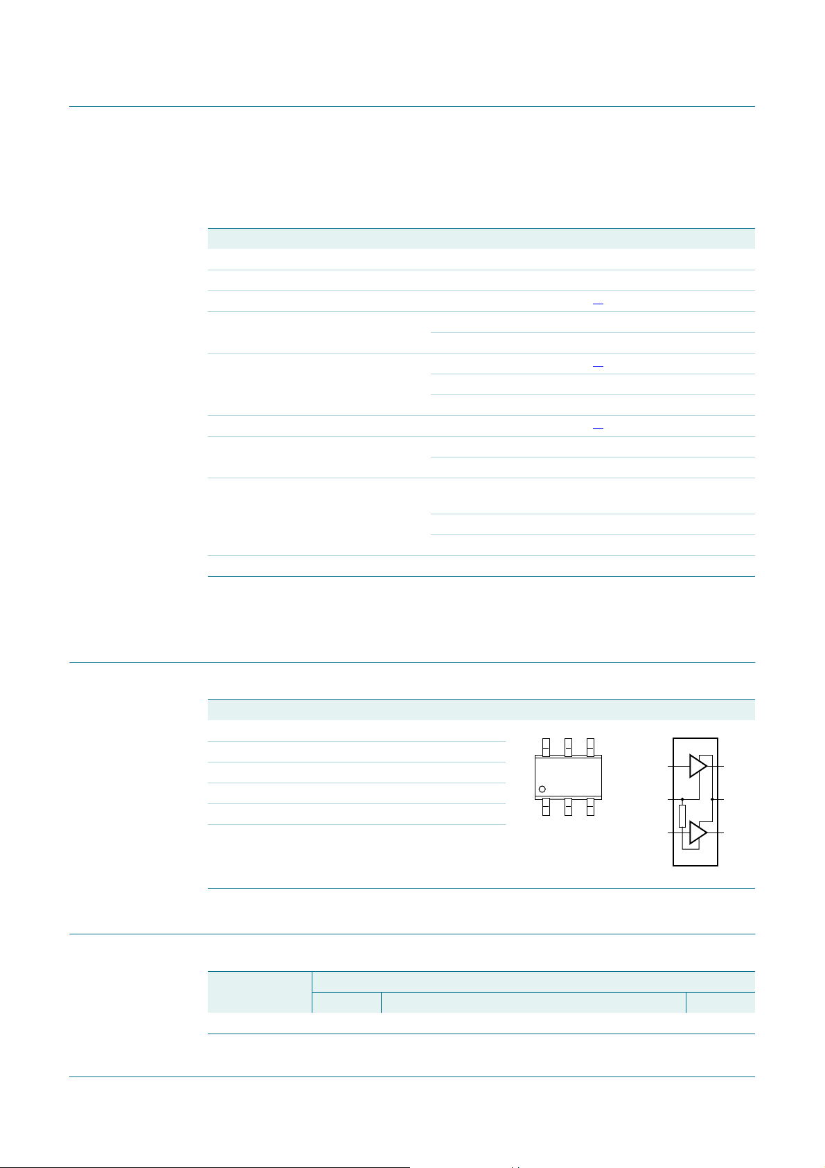
2. Pinning information
Table 2. Discrete pinning
Pin Description Simplified outline Symbol
1 gate1 (AMP A)
2 gate2
3 gate1 (AMP B)
4 drain (AMP B)
5 source
6 drain (AMP A)
3. Ordering information
Table 3. Ordering information
Type number Package
BF1210 - plastic surface-mounted package; 6 leads SOT363
56
4
132
AMP A
G1A
G2
G1B
AMP B
sym119
Name Description Version
DA
S
DB
BF1210_1 © NXP B.V. 2006. All rights reserved.
Product data sheet Rev. 01 — 25 October 2006 2 of 21
Page 3
NXP Semiconductors
4. Marking
Table 4. Marking
Type number Marking Description
BF1210 *AB * = p : made in Hong Kong
5. Limiting values
Table 5. Limiting values
In accordance with the Absolute Maximum Rating System (IEC 60134).
Symbol Parameter Conditions Min Max Unit
Per MOSFET
V
DS
I
D
I
G1
I
G2
P
tot
T
stg
T
j
[1] Tsp is the temperature at the soldering point of the source lead.
BF1210
Dual N-channel dual gate MOSFET
* = t : made in Malaysia
* = w : made in China
drain-source voltage - 6 V
drain current DC - 30 mA
gate1 current - ±10 mA
gate2 current - ±10 mA
total power dissipation Tsp≤ 107 °C
storage temperature −65 +150 °C
junction temperature - 150 °C
[1]
- 180 mW
250
P
tot
(mW)
200
150
100
50
0
0 20015050 100
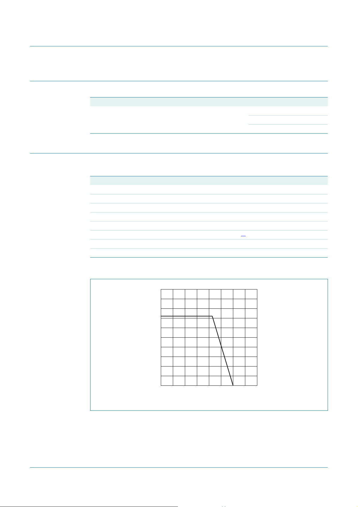
Fig 1. Power derating curve
001aac193
Tsp (˚C)
BF1210_1 © NXP B.V. 2006. All rights reserved.
Product data sheet Rev. 01 — 25 October 2006 3 of 21
Page 4
NXP Semiconductors
BF1210
Dual N-channel dual gate MOSFET
6. Thermal characteristics
Table 6. Thermal characteristics
Symbol Parameter Conditions Typ Unit
R
th(j-sp)
thermal resistance from junction to solder point 240 K/W
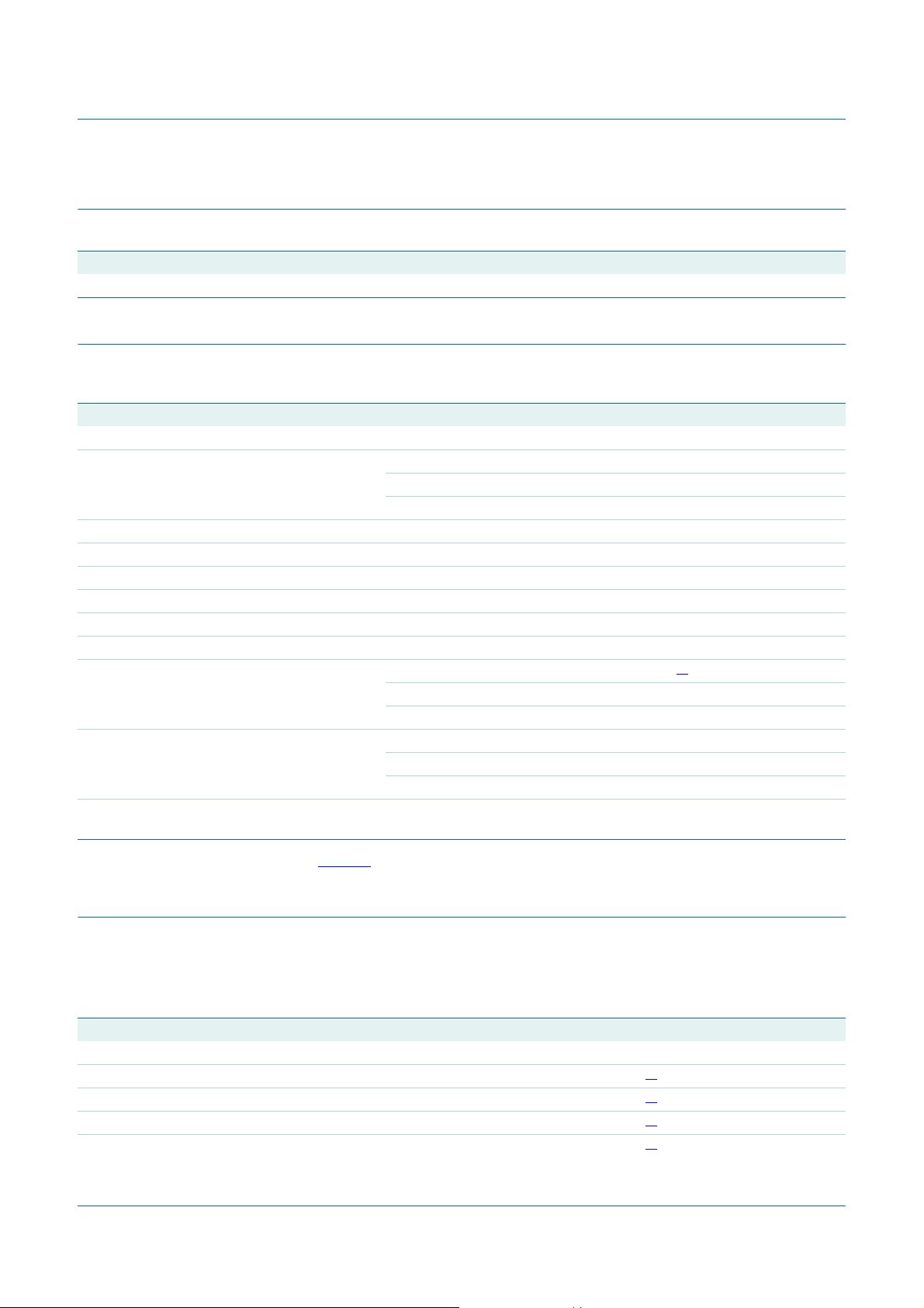
7. Static characteristics
Table 7. Static characteristics
Tj=25°C.
Symbol Parameter Conditions Min Typ Max Unit
Per MOSFET; unless otherwise specified
V
(BR)DSS
V
(BR)G1-SS
V
(BR)G2-SS
V
F(S-G1)
V
F(S-G2)
V
G1-S(th)
V
G2-S(th)
I
DS
I
G1-S
I
G2-S
drain-source breakdown voltage V
G1-S=VG2-S
amplifier A 6 - - V
amplifier B 6 - - V
gate1-source breakdown voltage V
gate2-source breakdown voltage V
forward source-gate1 voltage V
forward source-gate2 voltage V
G2-S=VDS
G1-S=VDS
G2-S=VDS
G1-S=VDS
gate1-source threshold voltage VDS=5V; V
gate2-source threshold voltage VDS=5V; V
drain-source current V
G2-S
=4V
amplifier A; V
amplifier B; V
gate1 cut-off current V
G2-S
=0V; V
amplifier A; V
amplifier B; V
gate2 cut-off current V
=4V; V
G2-S
V
G1-S(A)=VG1-S(B)
=0V; ID=10µA
=0V; I
=0V; I
=0V; I
=0V; I
G2-S
G1-S
DS(A)
DS(B)
DS(A)=VDS(B)
G1-S(A)
G1-S(B)
DS(A)=VDS(B)
=10mA 6 - 10 V
G1-S
=10mA 6 - 10 V
G2-S
= 10 mA 0.5 - 1.5 V
S-G1
= 10 mA 0.5 - 1.5 V
S-G2
=4V; ID= 100 µA 0.3 - 1.0 V
=5V; ID= 100 µA 0.4 - 1.0 V
[1]
=5V; R
=5V; R
=59kΩ 14 - 24 mA
G1(A)
= 150 kΩ 9 - 17 mA
G1(B)
=0V
=5V - - 50 nA
=5V - - 50 nA
=0V;
- - 20 nA
=0V
[1] RG1 connects gate1 to VGG = 5 V. See Figure 32.
8. Dynamic characteristics
8.1 Dynamic characteristics for amplifier A
Table 8. Dynamic characteristics for amplifier A
Common source; T
Symbol Parameter Conditions Min Typ Max Unit
| forward transfer admittance Tj=25°C263141mS
|y
fs
C
iss(G1)
C
iss(G2)
C
oss
C
rss
BF1210_1 © NXP B.V. 2006. All rights reserved.
Product data sheet Rev. 01 — 25 October 2006 4 of 21
input capacitance at gate1 f = 100 MHz
input capacitance at gate2 f = 100 MHz
output capacitance f = 100 MHz
reverse transfer capacitance f = 100 MHz
=25°C; V
amb
G2-S
=4V; V
DS(A)
=5V; I
D(A)
=19mA.
[1]
- 2.2 2.7 pF
[1]
- 3.0 - pF
[1]
- 0.9 - pF
[1]
-20-fF
Page 5
NXP Semiconductors
BF1210
Dual N-channel dual gate MOSFET
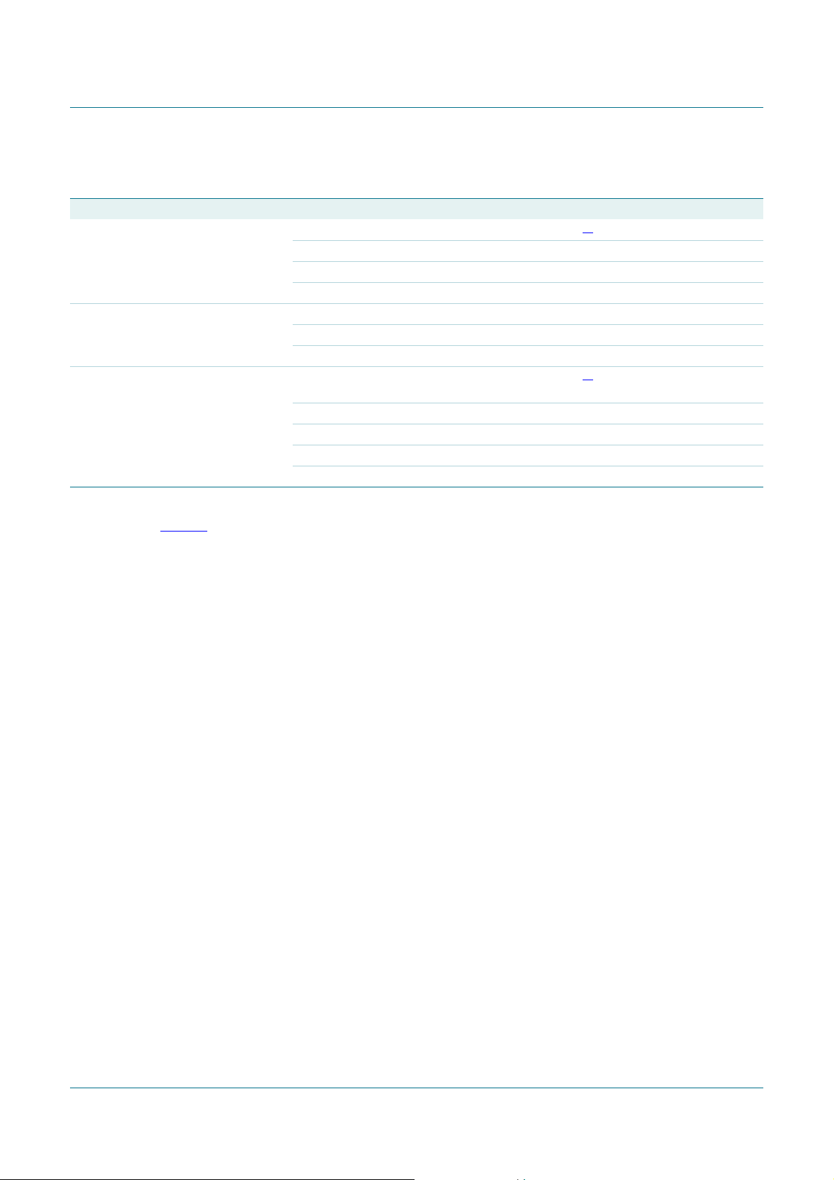
Table 8. Dynamic characteristics for amplifier A
Common source; T
=25°C; V
amb
G2-S
=4V; V
DS(A)
…continued
=5V; I
D(A)
=19mA.
Symbol Parameter Conditions Min Typ Max Unit
G
tr
transducer power gain BS=B
S(opt)
; BL=B
L(opt)
[1]
f = 200 MHz; GS= 2 mS; GL= 0.5 mS 31 35 39 dB
f = 400 MHz; G
f = 800 MHz; G
NF noise figure f = 11 MHz; G
f = 400 MHz; Y
f = 800 MHz; Y
Xmod cross modulation input level for k = 1 %; f
f
=60MHz
unw
= 2 mS; GL= 1 mS 27 31 35 dB
S
= 3.3 mS; GL=1mS 22 26 30 dB
S
= 20 mS; BS= 0 S - 3 - dB
S
S=YS(opt)
S=YS(opt)
= 50 MHz;
w
- 0.9 1.5 dB
- 1.2 1.9 dB
[2]
at 0 dB AGC 90 - - dBµV
at 10 dB AGC - 90 - dBµV
at 20 dB AGC - 99 - dBµV
at 40 dB AGC 100 105 - dBµV
[1] Calculated from S-parameters.
[2] Measured in Figure 32 test circuit.
BF1210_1 © NXP B.V. 2006. All rights reserved.
Product data sheet Rev. 01 — 25 October 2006 5 of 21
Page 6
NXP Semiconductors
8.1.1 Graphs for amplifier A
BF1210
Dual N-channel dual gate MOSFET
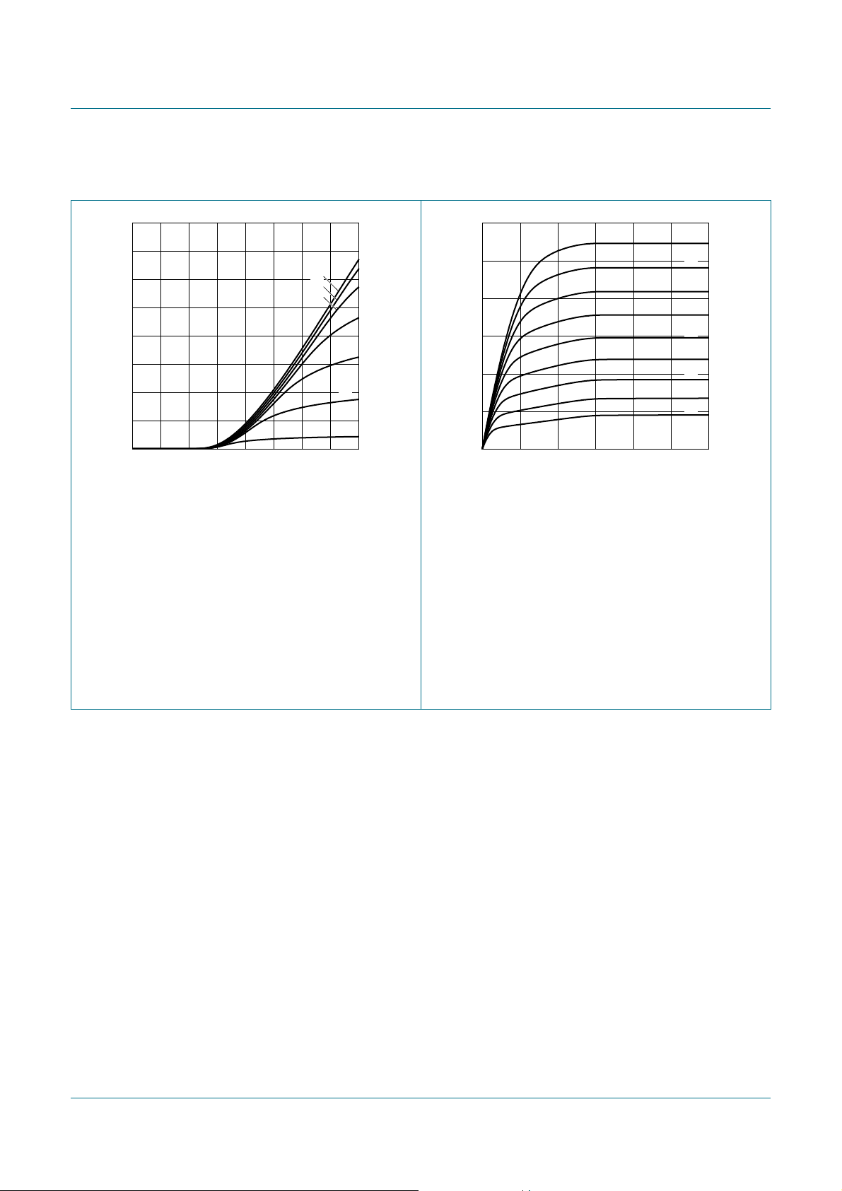
40
I
D
(mA)
30
20
10
0
0 2.01.50.5 1.0
(1) V
(2) V
(3) V
(4) V
(5) V
(6) V
(7) V
= 4.0 V.
G2-S
= 3.5 V.
G2-S
= 3.0 V.
G2-S
= 2.5 V.
G2-S
= 2.0 V.
G2-S
= 1.5 V.
G2-S
= 1.0 V.
G2-S
V
=5V; Tj=25°C.
DS(A)
001aaf476
(1)
(2)
(3)
V
G1-S
(4)
(5)
(6)
(7)
(V)
Fig 2. Amplifier A: transfer characteristics; typical
values
30
I
D
(mA)
20
10
0
0642
(1) V
G1-S(A)
(2) V
G1-S(A)
(3) V
G1-S(A)
(4) V
G1-S(A)
(5) V
G1-S(A)
(6) V
G1-S(A)
(7) V
G1-S(A)
(8) V
G1-S(A)
(9) V
G1-S(A)
V
G2-S
= 1.8 V.
= 1.7 V.
= 1.6 V.
= 1.5 V.
= 1.4 V.
= 1.3 V.
= 1.2 V.
= 1.1 V.
= 1.0 V.
=4V; Tj=25°C.
001aaf477
(1)
(2)
(3)
(4)
(5)
(6)
(7)
(8)
(9)
VDS (V)
Fig 3. Amplifier A: output characteristics; typical
values
BF1210_1 © NXP B.V. 2006. All rights reserved.
Product data sheet Rev. 01 — 25 October 2006 6 of 21
Page 7
NXP Semiconductors
BF1210
Dual N-channel dual gate MOSFET
100
I
G1
(µA)
80
60
40
20
0
0 2.01.50.5 1.0
(1) V
(2) V
(3) V
(4) V
(5) V
(6) V
(7) V
= 4.0 V.
G2-S
= 3.5 V.
G2-S
= 3.0 V.
G2-S
= 2.5 V.
G2-S
= 2.0 V.
G2-S
= 1.5 V.
G2-S
= 1.0 V.
G2-S
V
=5V; Tj=25°C.
DS(A)
001aaf478
V
G1-S
(1)
(2)
(3)
(4)
(5)
(6)
(7)
(V)
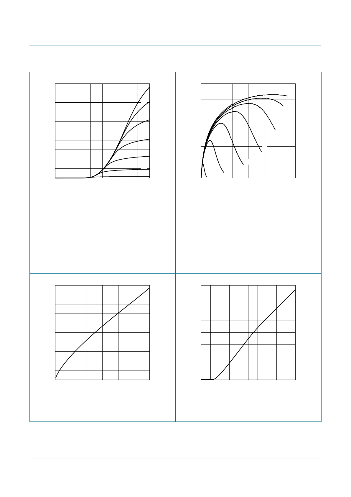
Fig 4. Amplifier A: gate1 current as a function of
gate1 voltage; typical values
36
Y
fs
(mS)
24
12
0
0362412
(1) V
G2-S
(2) V
G2-S
(3) V
G2-S
(4) V
G2-S
(5) V
G2-S
(6) V
G2-S
(7) V
G2-S
V
DS(A)
(5)
(6)
(7)
= 4.0 V.
= 3.5 V.
= 3.0 V.
= 2.5 V.
= 2.0 V.
= 1.5 V.
= 1.0 V.
=5V; Tj=25°C.
001aaf479
(1)
(2)
(3)
(4)
ID (mA)
Fig 5. Amplifier A: forward transfer admittance as a
function of drain current; typical values
20
I
D
(mA)
16
12
8
4
0
0604020
V
DS(A)
=5V; V
=4V; Tj=25°C. V
G2-S
001aaf480
IG1 (µA)
Fig 6. AmplifierA: drain current as a function of gate1
current; typical values
001aaf481
VGG (V)
=59kΩ;Tj=25°C.
I
D
(mA)
20
15
10
5
0
054231
DS(A)
=5V;V
G2-S
=4V;R
G1(A)
Fig 7. AmplifierA: drain current as a function of gate1
supply voltage (V
); typical values
GG
BF1210_1 © NXP B.V. 2006. All rights reserved.
Product data sheet Rev. 01 — 25 October 2006 7 of 21
Page 8
NXP Semiconductors
BF1210
Dual N-channel dual gate MOSFET
V
GG
001aaf482
(1)
(2)
(3)
(4)
(5)
(6)
(7)
= VDS (V)
25
I
D
(mA)
20
15
10
(1) R
(2) R
(3) R
(4) R
(5) R
(6) R
(7) R
5
0
054231
=47kΩ.
G1(A)
=59kΩ.
G1(A)
=68kΩ.
G1(A)
=82kΩ.
G1(A)
= 100 kΩ.
G1(A)
= 120 kΩ.
G1(A)
= 150 kΩ.
G1(A)
V
=4V; Tj=25°C.
G2-S
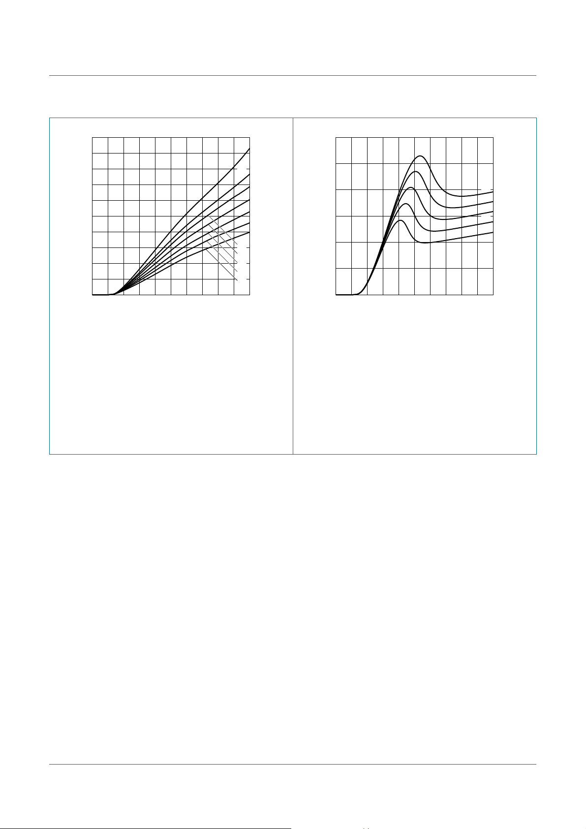
Fig 8. Amplifier A: drain current as a function of V
and VGG; typical values
30
I
D
(mA)
20
10
0
054231
V
(1) VGG= 5.0 V.
(2) VGG= 4.5 V.
(3) VGG= 4.0 V.
(4) VGG= 3.5 V.
(5) VGG= 3.0 V.
Tj=25°C; R
Fig 9. AmplifierA: drain current as a function of gate2
DS
=59kΩ (connected to VGG).
G1(A)
voltage; typical values
001aaf483
(1)
(2)
(3)
(4)
(5)
(V)
G2-S
BF1210_1 © NXP B.V. 2006. All rights reserved.
Product data sheet Rev. 01 — 25 October 2006 8 of 21
Page 9
NXP Semiconductors
BF1210
Dual N-channel dual gate MOSFET
0
gain
reduction
(dB)
10
20
30
40
50
04312
V
=5V; VGG=5V; I
DS(A)
R
=59kΩ; f = 50 MHz; T
G1(A)
D(nom)(A)
amb
001aaf484
V
AGC
=19mA;
=25°C;
(V)
see Figure 32.
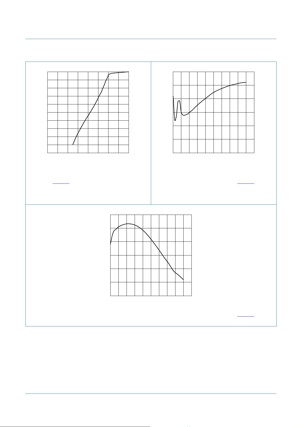
Fig 10. Amplifier A: typical gain reduction as a function
of the AGC voltage; typical values
30
110
V
unw
(dBµV)
100
90
80
0504020 3010
V
=5V; VGG=5V; V
DS(A)
R
=59kΩ; fw= 50 MHz; f
G1(A)
I
D(nom)(A)
= 19 mA; T
G2-S(nom)
unw
=25°C; see Figure 32.
amb
001aaf485
gain reduction (dB)
=4V;
= 60 MHz;
Fig 11. Amplifier A: unwanted voltage for 1 %
cross modulation as a function of gain
reduction; typical values
001aaf486
I
D
(mA)
20
10
0
V
=5V; VGG=5V; V
DS(A)
G2-S(nom)
0504020 3010
=4V; R
=59kΩ; f = 50 MHz; I
G1(A)
gain reduction (dB)
D(nom)(A)
= 19 mA; T
amb
Fig 12. Amplifier A: typical drain current as a function of gain reduction; typical values
=25°C; see Figure 32.
BF1210_1 © NXP B.V. 2006. All rights reserved.
Product data sheet Rev. 01 — 25 October 2006 9 of 21
Page 10
NXP Semiconductors
BF1210
Dual N-channel dual gate MOSFET
2
10
bis, g
is
(mS)
10
b
is
1
g
2
10
=4V; V
is
DS(B)
−1
10
−2
10
10 10
V
=5V; V
I
D(A)
DS(A)
= 19 mA.
G2-S
001aaf487
3
f (MHz)
=0V;
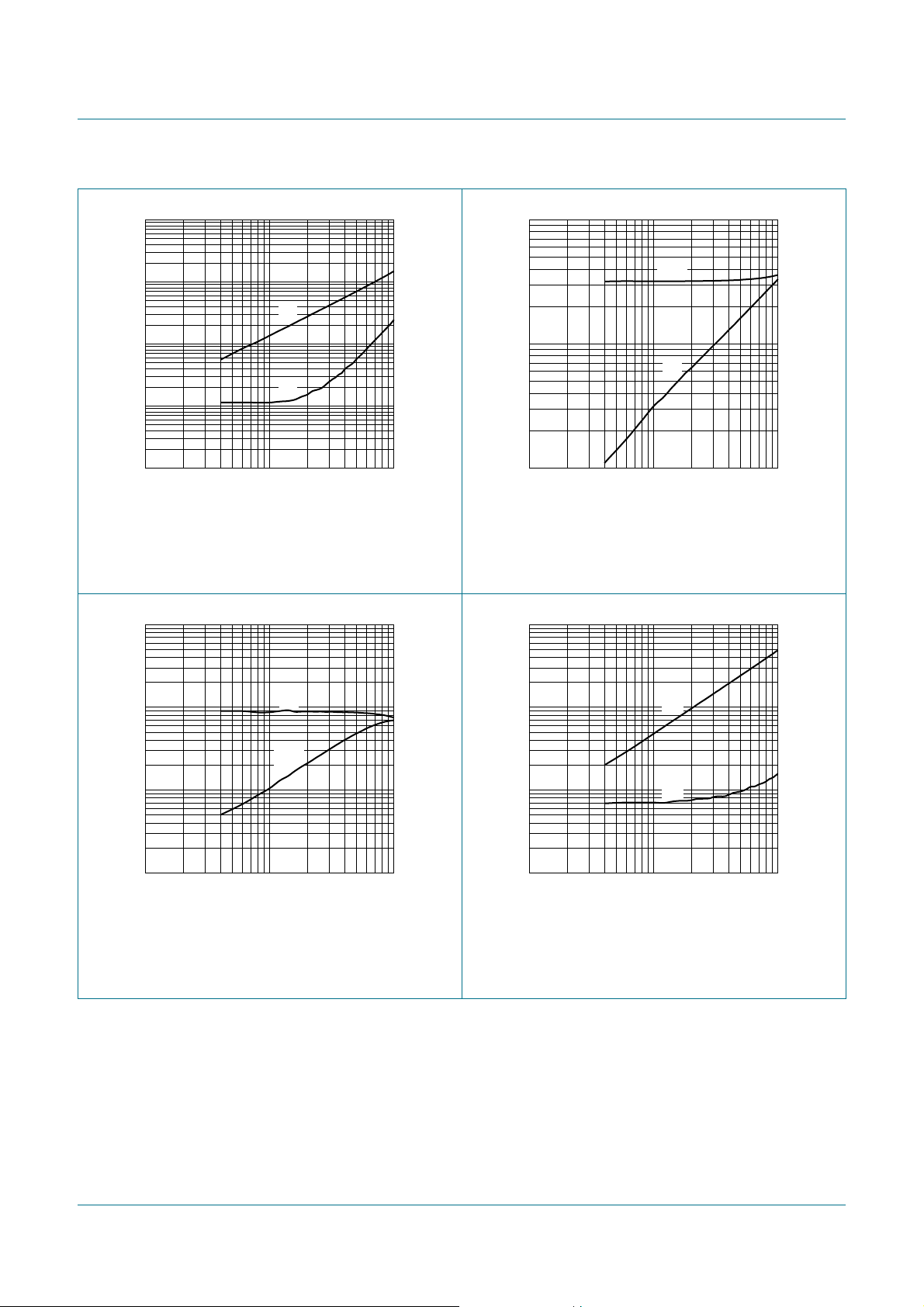
Fig 13. Amplifier A: input admittance as a function of
frequency; typical values
10
Yrs
(µS)
3
001aaf489
−10
(deg)
3
ϕ
rs
2
10
Yfs
(mS)
10
1
10 10
V
=5V; V
I
D(A)
DS(A)
= 19 mA.
G2-S
Yfs
2
10
=4V; V
ϕ
fs
DS(B)
f (MHz)
=0V;
001aaf488
−10
−10
−1
3
2
ϕ
fs
(deg)
Fig 14. Amplifier A: forward transfer admittance and
phase as a function of frequency; typical values
001aaf490
b
os
(mS)
10
, g
os
ϕ
Yrs
2
10
=4V; V
rs
DS(B)
−10
−10
3
f (MHz)
=0V;
2
10
10
1 −1
10 10
V
=5V; V
I
D(A)
DS(A)
= 19 mA.
G2-S
Fig 15. Amplifier A: reverse transfer admittance and
phase as a function of frequency; typical values
2
1
-1
10
-2
10
10 10
V
=5V; V
I
D(A)
DS(A)
= 19 mA.
G2-S
2
10
=4V; V
b
g
os
os
DS(B)
f (MHz)
3
=0V;
Fig 16. Amplifier A: output admittance as a function of
frequency; typical values
BF1210_1 © NXP B.V. 2006. All rights reserved.
Product data sheet Rev. 01 — 25 October 2006 10 of 21
Page 11
NXP Semiconductors
BF1210
Dual N-channel dual gate MOSFET
8.1.2 Scattering parameters for amplifier A
Table 9. Scattering parameters for amplifier A
V
=5V; V
DS(A)
f (MHz) s
Magnitude
(ratio)
40 0.9861 −3.2 3.14 176.75 0.00054 87.97 0.9934 −1.19
100 0.9883 −7.84 3.14 171.53 0.00104 87.69 0.9925 −2.85
200 0.9844 −15.7 3.12 163.1 0.00205 80.77 0.9918 −5.69
300 0.9761 −23.52 3.08 154.65 0.00295 76.33 0.9904 −8.51
400 0.9635 −31.26 3.03 146.33 0.00375 72.34 0.9888 −11.33
500 0.9486 −38.78 2.97 138.15 0.00437 67.97 0.9870 −14.13
600 0.9305 −46.2 2.90 130.12 0.00483 64.86 0.9847 −16.87
700 0.9105 −53.33 2.81 122.26 0.0051 62.13 0.9832 −19.61
800 0.8911 −60.2 2.73 114.65 0.0052 59.88 0.9817 −22.35
900 0.8723 −67.03 2.65 107.2 0.00515 58.8 0.9796 −25.03
1000 0.8521 −73.74 2.56 99.78 0.00498 58.03 0.9785 −27.08
11
G2-S
=4V; I
= 19 mA; V
D(A)
Angle
(deg)
=0V;V
DS(B)
s
21
Magnitude
(ratio)
G1-S(B)
Angle
(deg)
=0V; T
s
Magnitude
(ratio)
=25°C; typical values.
amb
12
Angle
(deg)
s
22
Magnitude
(ratio)
Angle
(deg)
8.2 Noise data for amplifier A
Table 10. Noise data for amplifier A
V
=5V; V
DS(A)
f (MHz) NF
G2-S
=4V; I
= 19 mA, T
D(A)
(dB) Γ
min
=25°C; typical values.
amb
opt
rn (ratio)
(ratio) (deg)
400 0.9 0.749 23.7 0.667
800 1.2 0.688 48.65 0.583
8.3 Dynamic characteristics for amplifier B
Table 11. Dynamic characteristics for amplifier B
Common source; T
Symbol Parameter Conditions Min Typ Max Unit
| forward transfer admittance Tj=25°C283343mS
|y
fs
C
iss(G1)
C
iss(G2)
C
oss
C
rss
G
tr
input capacitance at gate1 f = 100 MHz
input capacitance at gate2 f = 100 MHz
output capacitance f = 100 MHz
reverse transfer capacitance f = 100 MHz
transducer power gain BS=B
NF noise figure f = 11 MHz; G
=25°C; V
amb
G2-S
=4V; V
DS(B)
S(opt)
=5V; I
; BL=B
D(B)
L(opt)
=13mA.
[1]
- 1.9 2.4 pF
[1]
- 3.4 - pF
[1]
- 0.85 - pF
[1]
-20-fF
[1]
f = 200 MHz; GS= 2 mS; GL= 0.5 mS 32 36 40 dB
f = 400 MHz; G
f = 800 MHz; G
f = 400 MHz; Y
f = 800 MHz; Y
= 2 mS; GL= 1 mS 29 33 37 dB
S
= 3.3 mS; GL=1mS 27 31 35 dB
S
= 20 mS; BS=0S - 4 - dB
S
S=YS(opt)
S=YS(opt)
- 0.9 1.5 dB
- 1.2 1.9 dB
BF1210_1 © NXP B.V. 2006. All rights reserved.
Product data sheet Rev. 01 — 25 October 2006 11 of 21
Page 12
NXP Semiconductors
BF1210
Dual N-channel dual gate MOSFET
Table 11. Dynamic characteristics for amplifier B
Common source; T
=25°C; V
amb
G2-S
=4V; V
DS(B)
…continued
=5V; I
D(B)
=13mA.
Symbol Parameter Conditions Min Typ Max Unit
Xmod cross modulation input level for k= 1 %; fw= 50 MHz;
f
=60MHz
unw
[2]
at 0 dB AGC 90 - - dBµV
at 10 dB AGC - 88 - dBµV
at 20 dB AGC - 94 - dBµV
at 40 dB AGC 100 103 - dBµV
[1] Calculated from S-parameters.
[2] Measured in Figure 32 test circuit.
8.3.1 Graphs for amplifier B
I
D
(mA)
50
40
30
001aaf491
(1)
(2)
(3)
(4)
I
D
(mA)
30
20
001aaf492
(1)
(2)
(3)
(4)
V
G1-S
(5)
(6)
(7)
(V)
20
10
0
0 2.01.50.5 1.0
(1) V
(2) V
(3) V
(4) V
(5) V
(6) V
(7) V
=4V.
G2-S
= 3.5 V.
G2-S
=3V.
G2-S
= 2.5 V.
G2-S
=2V.
G2-S
= 1.5 V.
G2-S
=1V.
G2-S
V
=5V; Tj=25°C.
DS(B)
Fig 17. Amplifier B: transfer characteristics; typical
values
(5)
10
0
0642
(1) V
G1-S(B)
(2) V
G1-S(B)
(3) V
G1-S(B)
(4) V
G1-S(B)
(5) V
G1-S(B)
(6) V
G1-S(B)
(7) V
G1-S(B)
V
G2-S
= 1.6 V.
= 1.5 V.
= 1.4 V.
= 1.3 V.
= 1.2 V.
= 1.1 V.
= 1.0 V.
=4V; Tj=25°C.
(6)
(7)
VDS (V)
Fig 18. Amplifier B: output characteristics; typical
values
BF1210_1 © NXP B.V. 2006. All rights reserved.
Product data sheet Rev. 01 — 25 October 2006 12 of 21
Page 13
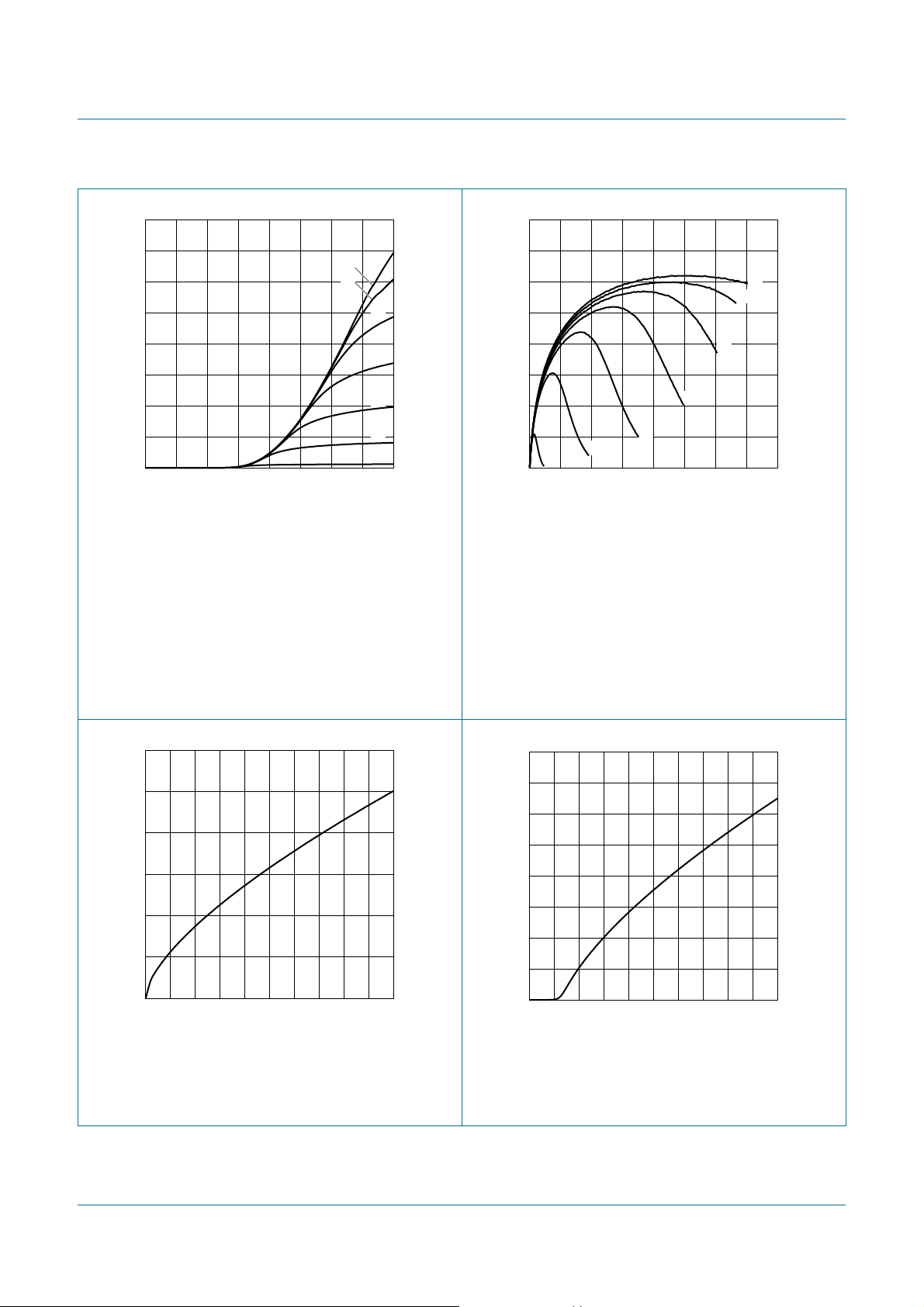
NXP Semiconductors
BF1210
Dual N-channel dual gate MOSFET
160
I
G1
(µA)
120
80
40
0
0 2.01.50.5 1.0
(1) V
(2) V
(3) V
(4) V
(5) V
(6) V
(7) V
=4V.
G2-S
= 3.5 V.
G2-S
=3V.
G2-S
= 2.5 V.
G2-S
=2V.
G2-S
= 1.5 V.
G2-S
=1V.
G2-S
V
=5V; Tj=25°C.
DS(B)
001aaf493
(1)
(2)
V
G1-S
(3)
(4)
(5)
(6)
(7)
(V)
Fig 19. Amplifier B: gate1 current as a function of
gate1 voltage; typical values
48
Y
fs
(mS)
36
24
12
(7)
0
0483612 24
(1) V
(2) V
(3) V
(4) V
(5) V
(6) V
(7) V
=4V.
G2-S
= 3.5 V.
G2-S
=3V.
G2-S
= 2.5 V.
G2-S
=2V.
G2-S
= 1.5 V.
G2-S
=1V.
G2-S
V
=5V; Tj=25°C.
DS(B)
(4)
(5)
(6)
001aaf494
(1)
(2)
(3)
ID (mA)
Fig 20. Amplifier B: forward transfer admittance as a
function of drain current; typical values
001aaf495
IG1 (µA)
I
D
(mA)
24
16
8
0
0504020 3010
V
DS(B)
=5V; V
=4V; Tj=25°C. V
G2-S
Fig 21. Amplifier B: drain current as a function of gate1
current; typical values
001aaf496
VGG (V)
= 150 kΩ;
I
D
(mA)
16
12
8
4
0
054231
DS(B)
=5V; V
G2-S
=4V; R
G1(B)
Tj=25°C.
Fig 22. Amplifier B: drain voltage as a function of gate1
supply voltage (V
); typical values
GG
BF1210_1 © NXP B.V. 2006. All rights reserved.
Product data sheet Rev. 01 — 25 October 2006 13 of 21
Page 14
NXP Semiconductors
BF1210
Dual N-channel dual gate MOSFET
25
I
D
(mA)
20
15
10
(1) R
(2) R
(3) R
(4) R
(5) R
(6) R
(7) R
5
0
054231
G1(B)
G1(B)
G1(B)
G1(B)
G1(B)
G1(B)
G1(B)
V
G2-S
=68kΩ.
=82kΩ.
= 100 kΩ.
= 120 kΩ.
= 150 kΩ.
= 180 kΩ.
= 220 kΩ.
=5V; R
connected to VGG; Tj=25°C.
G1(B)
001aaf497
(1)
(2)
(3)
(4)
(5)
(6)
(7)
VGG = VDS (V)
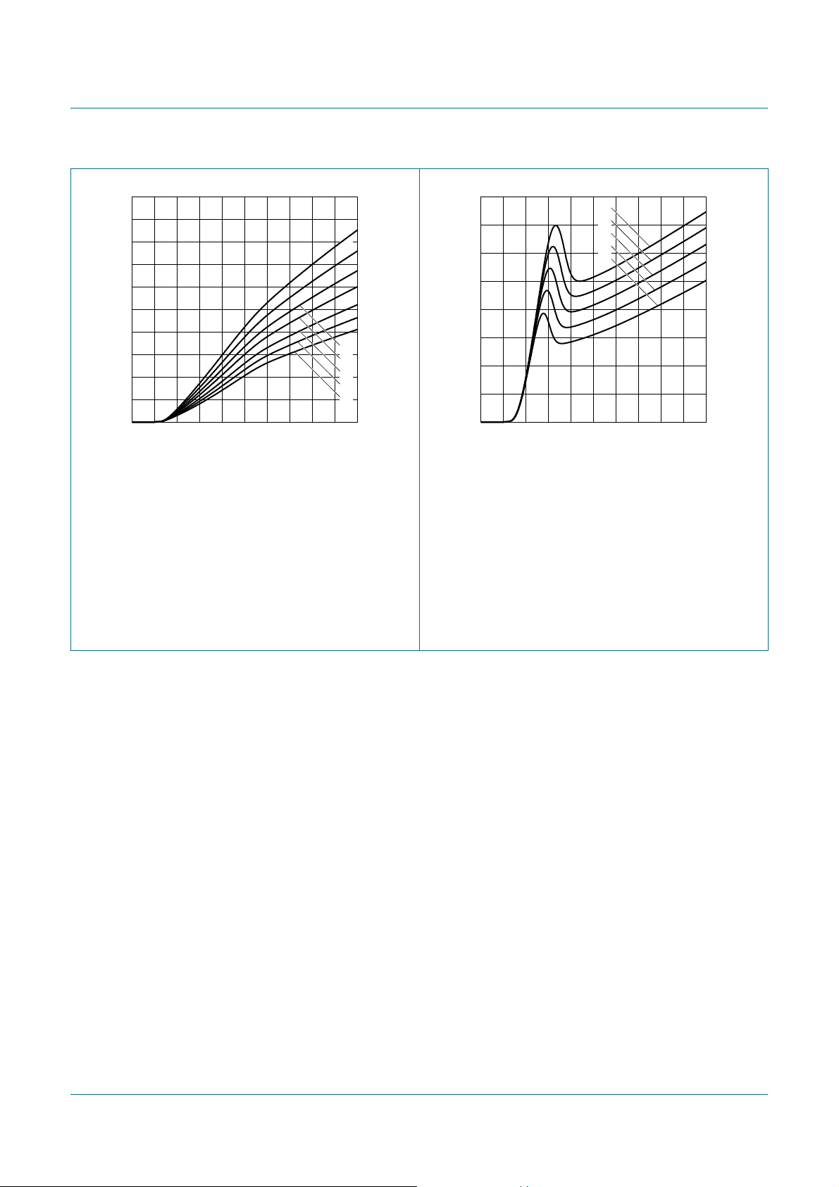
Fig 23. Amplifier B: drain current as a function of V
and VGG; typical values
I
D
(mA)
16
12
8
4
0
054231
(1)
(2)
(3)
(4)
(5)
V
(1) VGG= 5.0 V.
(2) VGG= 4.5 V.
(3) VGG= 4.0 V.
(4) VGG= 3.5 V.
(5) VGG= 3.0 V.
R
= 150 kΩ; Tj=25°C.
G1(B)
Fig 24. Amplifier B: drain current as a function of gate2
DS
voltage; typical values
001aaf498
(V)
G2-S
BF1210_1 © NXP B.V. 2006. All rights reserved.
Product data sheet Rev. 01 — 25 October 2006 14 of 21
Page 15
NXP Semiconductors
BF1210
Dual N-channel dual gate MOSFET
G1(B)
001aaf499
V
(V)
AGC
= 150 kΩ;
0
gain
reduction
(dB)
20
40
60
04312
V
=5V; V
DS(B)
I
D(nom)(B)
G2-S(nom)
= 13 mA; T
=4V; R
=25°C; see Figure 32.
amb
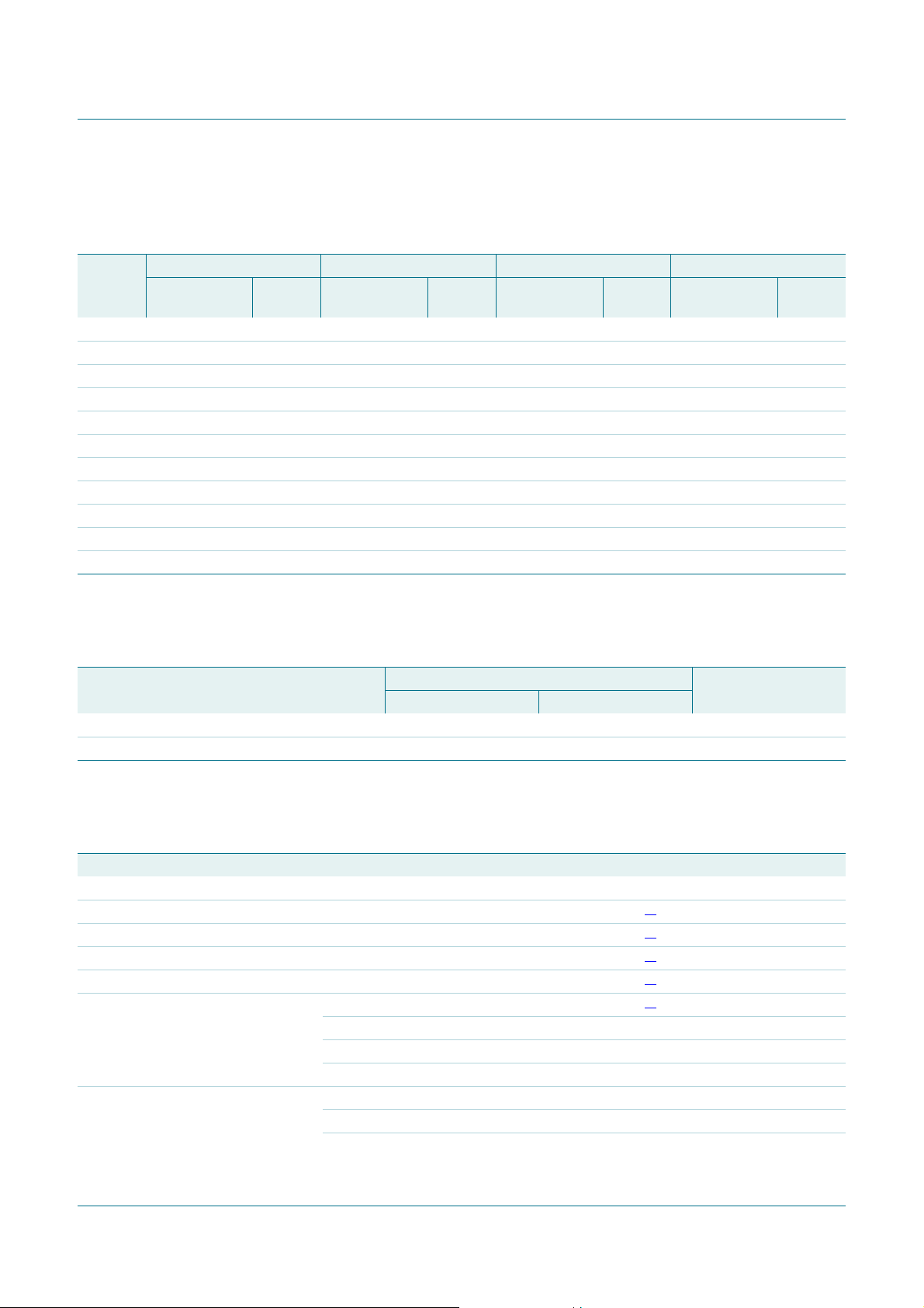
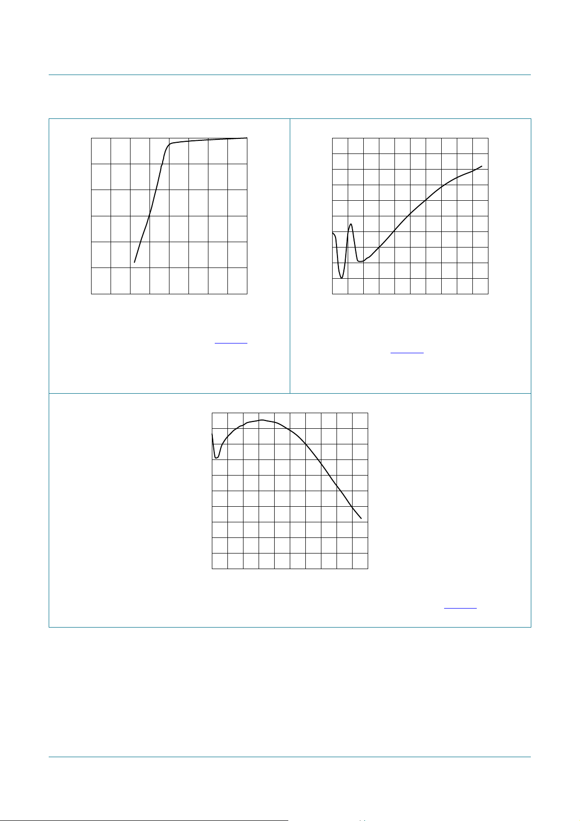
Fig 25. Amplifier B: typical gain reduction as a function
of the AGC voltage; typical values
15
I
D
(mA)
12
110
V
unw
(dBµV)
105
100
95
90
85
0504020 3010
V
=5V; V
DS(B)
I
D(nom)(B)
T
= 13 mA; fw= 50 MHz; f
=25°C; see Figure 32.
amb
G2-S(nom)
=4V; R
001aaf500
gain reduction (dB)
= 150 kΩ;
G1(B)
= 60 MHz;
unw
Fig 26. Amplifier B: unwanted voltage for 1 %
cross modulation as a function of gain
reduction; typical values
001aaf501
9
6
3
0
V
DS(B)=VGG
=5V; V
G2-S(nom)
0504020 3010
=4V; R
G1(B)
= 150 kΩ; I
D(nom)(B)
gain reduction (dB)
= 13 mA; f = 50 MHz; T
=25°C; see Figure 32.
amb
Fig 27. Amplifier B: typical drain current as a function of gain reduction; typical values
BF1210_1 © NXP B.V. 2006. All rights reserved.
Product data sheet Rev. 01 — 25 October 2006 15 of 21
Page 16
NXP Semiconductors
BF1210
Dual N-channel dual gate MOSFET
2
10
bis, g
is
(mS)
10
b
is
1
g
2
10
=4V; V
is
DS(A)
−1
10
−2
10
10 10
V
=5V; V
I
D(B)
DS(B)
= 13 mA.
G2-S
001aaf502
3
f (MHz)
=0V;
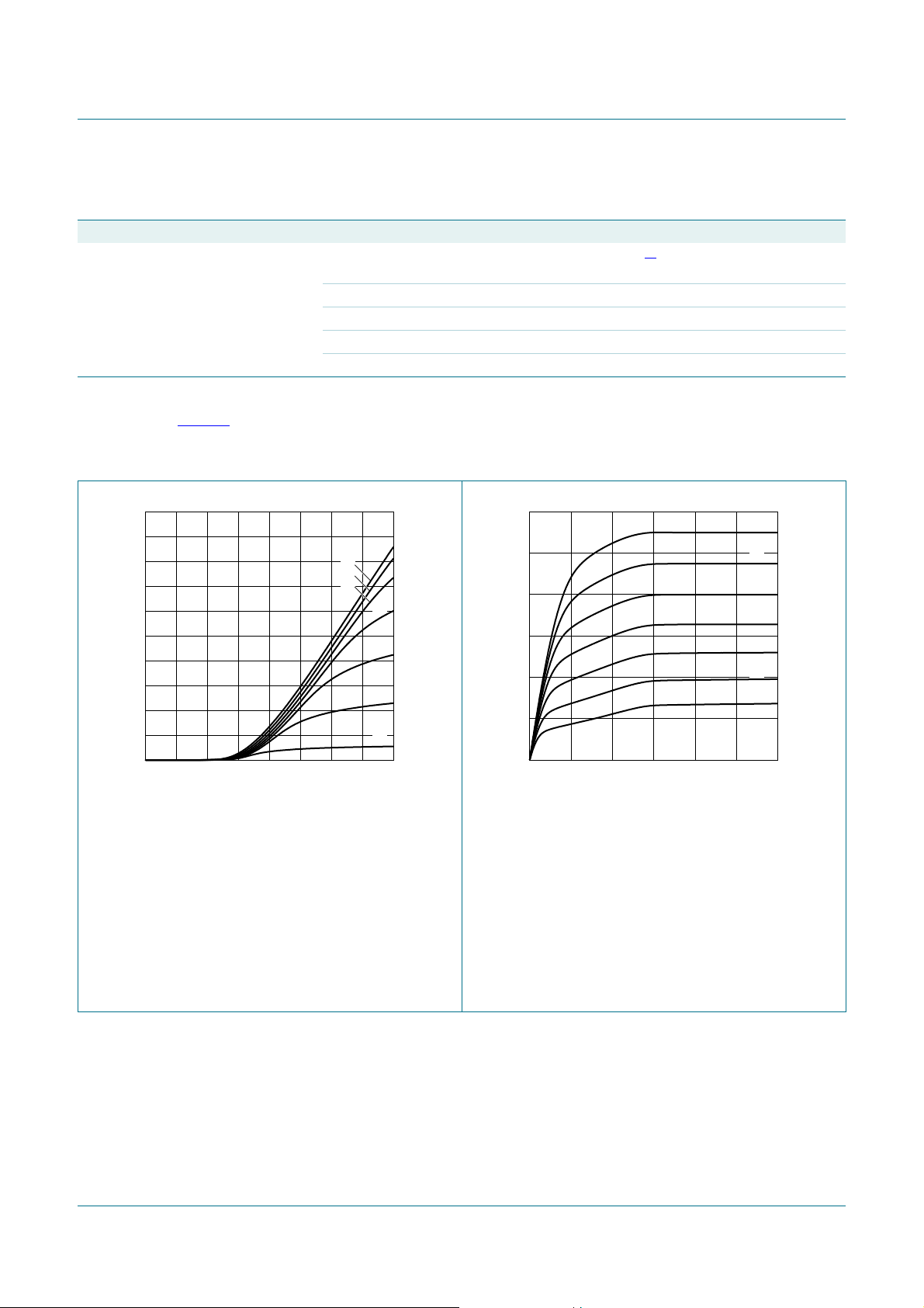
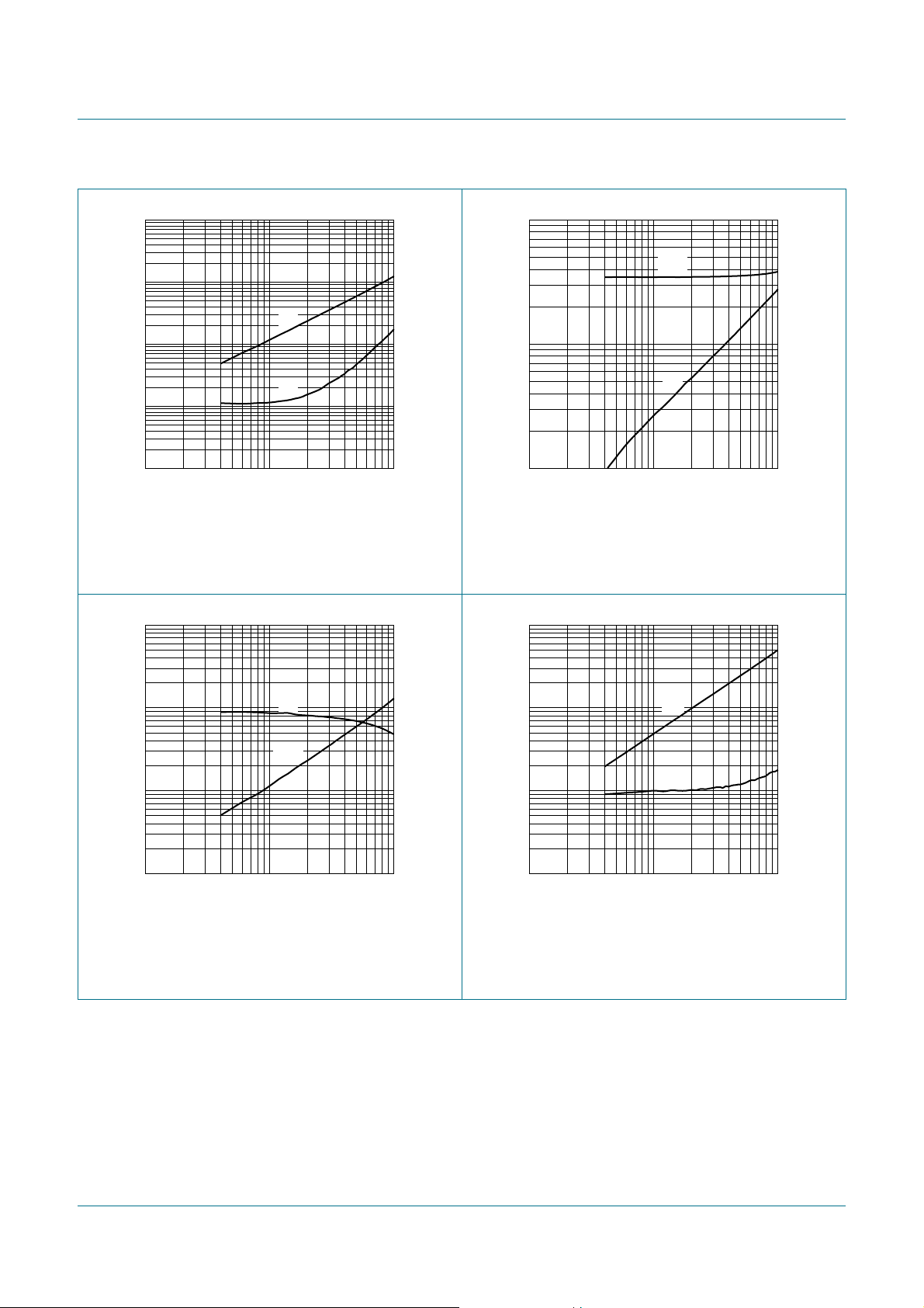
Fig 28. Amplifier B: input admittance as a function of
frequency; typical values
10
Yrs
(mS)
3
001aaf504
10
(deg)
3
ϕ
rs
2
10
Yfs
(mS)
10
1
10 10
V
=5V; V
I
D(B)
DS(B)
= 13 mA.
G2-S
Yfs
2
10
=4V; V
ϕ
fs
DS(A)
f (MHz)
=0V;
001aaf503
−10
−10
−1
3
2
ϕ
fs
(deg)
Fig 29. Amplifier B: forward transfer admittance and
phase as a function of frequency; typical values
001aaf505
b
os
(mS)
10
, g
os
Yrs
2
10
=4V; V
ϕ
rs
DS(A)
f (MHz)
=0V;
2
10
10
1
10 10
V
=5V; V
I
D(B)
DS(B)
= 13 mA.
G2-S
2
10
10
1
3
Fig 30. Amplifier B: reverse transfer admittance and
phase as a function of frequency; typical values
b
2
10
=4V; V
os
g
os
DS(A)
f (MHz)
3
=0V;
1
−1
10
−2
10
10 10
V
=5V; V
I
D(B)
DS(B)
= 13 mA.
G2-S
Fig 31. Amplifier B: output admittance as a function of
frequency; typical values
BF1210_1 © NXP B.V. 2006. All rights reserved.
Product data sheet Rev. 01 — 25 October 2006 16 of 21
Page 17
NXP Semiconductors
BF1210
Dual N-channel dual gate MOSFET
8.3.2 Scattering parameters for amplifier B
Table 12. Scattering parameters for amplifier B
V
=5V; V
DS(B)
f (MHz) s
Magnitude
(ratio)
40 0.9874 −2.79 3.41 177.08 0.00054 89.27 0.992 −1.26
100 0.9883 −6.8 3.41 172.57 0.00113 90.81 0.9900 −2.91
200 0.9844 −13.52 3.39 165.23 0.00224 89.67 0.9897 −5.81
300 0.9777 −20.2 3.36 157.88 0.00336 89.02 0.9889 −8.7
400 0.9684 −26.83 3.32 150.6 0.00447 88.43 0.9881 −11.61
500 0.9578 −33.32 3.27 143.38 0.0055 87.64 0.9870 −14.52
600 0.9442 −39.8 3.21 136.22 0.00649 87.53 0.9851 −17.39
700 0.9291 −46.08 3.16 129.15 0.00741 87.51 0.9838 −20.3
800 0.9147 −52.18 3.08 122.25 0.00828 87.7 0.9825 −23.2
900 0.9002 −58.35 3.08 115.4 0.00914 88.14 0.9803 −26.06
1000 0.8836 −64.49 2.93 108.49 0.00997 88.26 0.9789 −29.03
11
G2-S
=4V; I
= 13 mA; V
D(B)
Angle
(deg)
=0V;V
DS(A)
s
21
Magnitude
(ratio)
G1-S(A)
Angle
(deg)
=0V; T
s
Magnitude
(ratio)
=25°C; typical values.
amb
12
Angle
(deg)
s
22
Magnitude
(ratio)
Angle
(deg)
8.4 Noise data for amplifier B
Table 13. Noise data for amplifier B
V
=5V; V
DS(B)
f (MHz) NF
G2-S
=4V; I
= 13 mA, T
D(B)
(dB) Γ
min
=25°C; typical values.
amb
opt
rn (ratio)
(ratio) (deg)
400 0.9 0.743 20.27 0.65
800 1.2 0.687 42.08 0.581
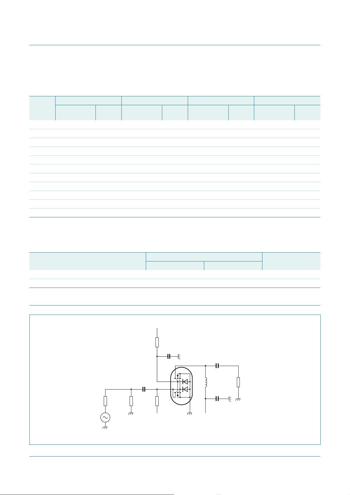
9. Test information
V
AGC
R1
10 kΩ
C1
C3
4.7 nF
L1
≈ 2.2 µH
C4
4.7 nF
R
L
50 Ω
R
GEN
50 Ω
R2
50 Ω
C2
4.7 nF
R
4.7 nF
DUT
G1
V
V
I
GG
V
DS
001aad926
Fig 32. Cross modulation test setup (for one MOSFET)
BF1210_1 © NXP B.V. 2006. All rights reserved.
Product data sheet Rev. 01 — 25 October 2006 17 of 21
Page 18
NXP Semiconductors
BF1210
Dual N-channel dual gate MOSFET
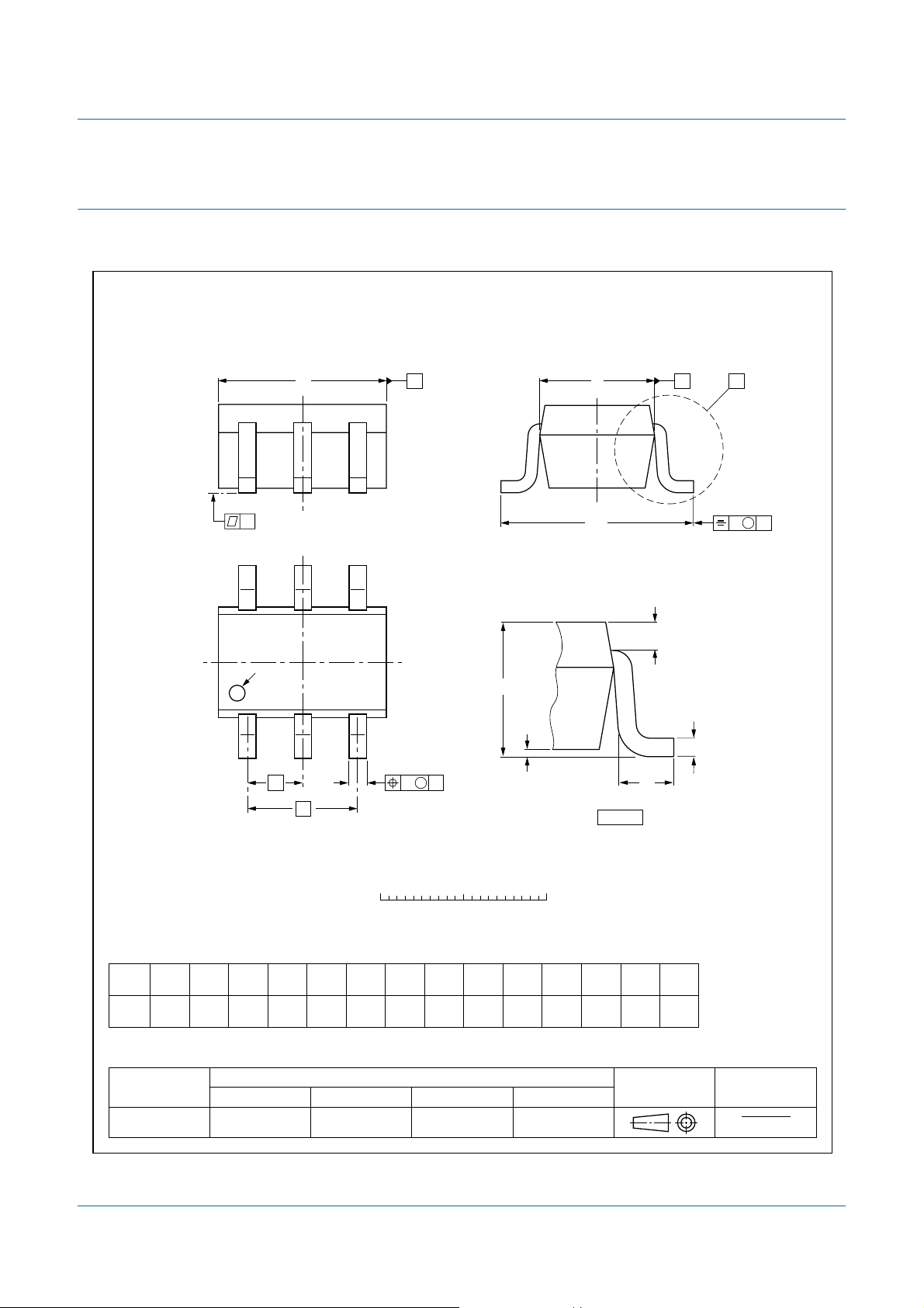
10. Package outline
Plastic surface-mounted package; 6 leads SOT363
D
y
pin 1
index
132
e
1
e
E
H
E
AB
X
v M
A
456
Q
A
A
1
b
p
wBM
L
detail X
c
p
0 1 2 mm
scale
DIMENSIONS (mm are the original dimensions)
A
1
UNIT
A
1.1
mm
0.8
OUTLINE
VERSION
SOT363 SC-88
max
0.1
b
cD
p
0.30
0.20
IEC JEDEC JEITA
0.25
0.10
2.2
1.8
E
1.35
1.3
1.15
REFERENCES
e
e
0.65
H
L
Qywv
p
E
1
2.2
0.45
2.0
0.15
0.25
0.15
0.2 0.10.2
EUROPEAN
PROJECTION
ISSUE DATE
04-11-08
06-03-16
Fig 33. Package outline SOT363
BF1210_1 © NXP B.V. 2006. All rights reserved.
Product data sheet Rev. 01 — 25 October 2006 18 of 21
Page 19
NXP Semiconductors
Dual N-channel dual gate MOSFET
BF1210
11. Abbreviations
Table 14. Abbreviations
Acronym Description
AGC Automatic Gain Control
DC Direct Current
MOSFET Metal-Oxide-Semiconductor Field-Effect Transistor
UHF Ultra High Frequency
VHF Very High Frequency
12. Revision history
Table 15. Revision history
Document ID Release date Data sheet status Change notice Supersedes
BF1210_1 20061025 Product data sheet - -
BF1210_1 © NXP B.V. 2006. All rights reserved.
Product data sheet Rev. 01 — 25 October 2006 19 of 21
Page 20

NXP Semiconductors
13. Legal information
13.1 Data sheet status
BF1210
Dual N-channel dual gate MOSFET
Document status
Objective [short] data sheet Development This document contains data from the objective specification for product development.
Preliminary [short] data sheet Qualification This document contains data from the preliminary specification.
Product [short] data sheet Production This document contains the product specification.
[1] Please consult the most recently issued document before initiating or completing a design.
[2] The term ‘short data sheet’ is explained in section “Definitions”.
[3] The product status of device(s) described in this documentmay have changed since this document was publishedand maydiffer in case of multiple devices.The latest product status
information is available on the Internet at URL
[1][2]
Product status
13.2 Definitions
Draft — The document is a draft version only. The content is still under
internal review and subject to formal approval, which may result in
modifications or additions. NXP Semiconductors does not give any
representations or warranties as to the accuracy or completeness of
information included herein and shallhave no liability for theconsequences of
use of such information.
Short data sheet — A short data sheet is an extract from a full data sheet
with thesame product typenumber(s) and title.A short data sheetis intended
for quick reference only and should not be relied upon to contain detailed and
full information. For detailed and full information see the relevant full data
sheet, which is available on request via the local NXP Semiconductors sales
office. In case of any inconsistency or conflict with the short data sheet, the
full data sheet shall prevail.
13.3 Disclaimers
General — Information in this document is believed to be accurate and
reliable. However,NXP Semiconductors does not giveany representations or
warranties, expressed or implied, asto the accuracy or completeness of such
information and shall have no liability for the consequences of use of such
information.
Right to make changes — NXP Semiconductors reserves the right to make
changes to information published in this document, including without
limitation specifications and product descriptions, at any time and without
notice. This document supersedes and replaces all informationsupplied prior
to the publication hereof.
Suitability for use — NXP Semiconductors products are not designed,
authorized or warranted to be suitable for use in medical, military, aircraft,
space or life support equipment, nor in applications where failure or
[3]
http://www.nxp.com.
Definition
malfunction of a NXP Semiconductors product can reasonably be expectedto
result in personal injury, death or severe property or environmental damage.
NXP Semiconductors accepts no liability for inclusion and/or use of NXP
Semiconductors products in such equipment or applications and therefore
such inclusion and/or use is at the customer’s own risk.
Applications — Applications that are described herein for any of these
products are for illustrative purposes only. NXP Semiconductors makes no
representation or warranty that such applications will be suitable for the
specified use without further testing or modification.
Limiting values — Stress above one or more limiting values (as defined in
the Absolute Maximum Ratings System of IEC 60134)may cause permanent
damage tothe device. Limitingvalues are stress ratings only and operationof
the device at these or any other conditions above those given in the
Characteristics sections of this document is not implied. Exposure to limiting
values for extended periods may affect device reliability.
Terms and conditions of sale — NXP Semiconductors products are sold
subject to the general terms and conditions of commercial sale, as published
at
http://www.nxp.com/profile/terms, including those pertaining to warranty,
intellectual property rights infringement and limitation of liability, unless
explicitly otherwise agreed to in writing by NXP Semiconductors. In case of
any inconsistency or conflict between information in this document and such
terms and conditions, the latter will prevail.
No offer to sell or license — Nothing in this document may be interpreted
or construed as an offer to sell products that is open for acceptance or the
grant, conveyance or implication of any license under any copyrights, patents
or other industrial or intellectual property rights.
13.4 Trademarks
Notice: All referenced brands,product names,service names and trademarks
are the property of their respective owners.
14. Contact information
For additional information, please visit: http://www.nxp.com
For sales office addresses, send an email to: [email protected]
BF1210_1 © NXP B.V. 2006. All rights reserved.
Product data sheet Rev. 01 — 25 October 2006 20 of 21
Page 21

NXP Semiconductors
15. Contents
1 Product profile . . . . . . . . . . . . . . . . . . . . . . . . . . 1
1.1 General description. . . . . . . . . . . . . . . . . . . . . . 1
1.2 Features . . . . . . . . . . . . . . . . . . . . . . . . . . . . . . 1
1.3 Applications . . . . . . . . . . . . . . . . . . . . . . . . . . . 1
1.4 Quick reference data. . . . . . . . . . . . . . . . . . . . . 2
2 Pinning information. . . . . . . . . . . . . . . . . . . . . . 2
3 Ordering information. . . . . . . . . . . . . . . . . . . . . 2
4 Marking. . . . . . . . . . . . . . . . . . . . . . . . . . . . . . . . 3
5 Limiting values. . . . . . . . . . . . . . . . . . . . . . . . . . 3
6 Thermal characteristics. . . . . . . . . . . . . . . . . . . 4
7 Static characteristics. . . . . . . . . . . . . . . . . . . . . 4
8 Dynamic characteristics . . . . . . . . . . . . . . . . . . 4
8.1 Dynamic characteristics for amplifier A. . . . . . . 4
8.1.1 Graphs for amplifier A. . . . . . . . . . . . . . . . . . . . 6
8.1.2 Scattering parameters for amplifier A. . . . . . . 11
8.2 Noise data for amplifier A . . . . . . . . . . . . . . . . 11
8.3 Dynamic characteristics for amplifier B. . . . . . 11
8.3.1 Graphs for amplifier B. . . . . . . . . . . . . . . . . . . 12
8.3.2 Scattering parameters for amplifier B. . . . . . . 17
8.4 Noise data for amplifier B . . . . . . . . . . . . . . . . 17
9 Test information. . . . . . . . . . . . . . . . . . . . . . . . 17
10 Package outline . . . . . . . . . . . . . . . . . . . . . . . . 18
11 Abbreviations. . . . . . . . . . . . . . . . . . . . . . . . . . 19
12 Revision history. . . . . . . . . . . . . . . . . . . . . . . . 19
13 Legal information. . . . . . . . . . . . . . . . . . . . . . . 20
13.1 Data sheet status . . . . . . . . . . . . . . . . . . . . . . 20
13.2 Definitions. . . . . . . . . . . . . . . . . . . . . . . . . . . . 20
13.3 Disclaimers. . . . . . . . . . . . . . . . . . . . . . . . . . . 20
13.4 Trademarks. . . . . . . . . . . . . . . . . . . . . . . . . . . 20
14 Contact information. . . . . . . . . . . . . . . . . . . . . 20
15 Contents. . . . . . . . . . . . . . . . . . . . . . . . . . . . . . 21
BF1210
Dual N-channel dual gate MOSFET
Please be aware that important notices concerning this document and the product(s)
described herein, have been included in section ‘Legal information’.
© NXP B.V. 2006. All rights reserved.
For more information, please visit: http://www.nxp.com
For sales office addresses, please send an email to: [email protected]
Date of release: 25 October 2006
Document identifier: BF1210_1
 Loading...