

Philips BF1107W, BF1107 Datasheet

DISCRETE SEMICONDUCTORS
DATA SH EET
BF1107; BF1107W
N-channel single gate MOS-FETs
Product specification
Supersedes data of 1998 Jun 22
1999 May 14
Philips Semiconductors Product specification
N-channel single gate MOS-FETs BF1107; BF1107W
FEATURES
• Currentless RF switch.
APPLICATIONS
• Various RF switching applications such as:
- Passive loop through for VCR tuner
- Transceiver switching.
DESCRIPTION
The BF1107 and BF1107W are depletion type field-effect
transistors in SOT23 and SOT323 packages respectively.
The low loss and high isolation capabilities of this
MOS-FET provide excellent RF switching functions.
Integrated diodes between gate and source and between
gate and drain protect against excessive input voltage
surges. Drain and source are interchangeable.
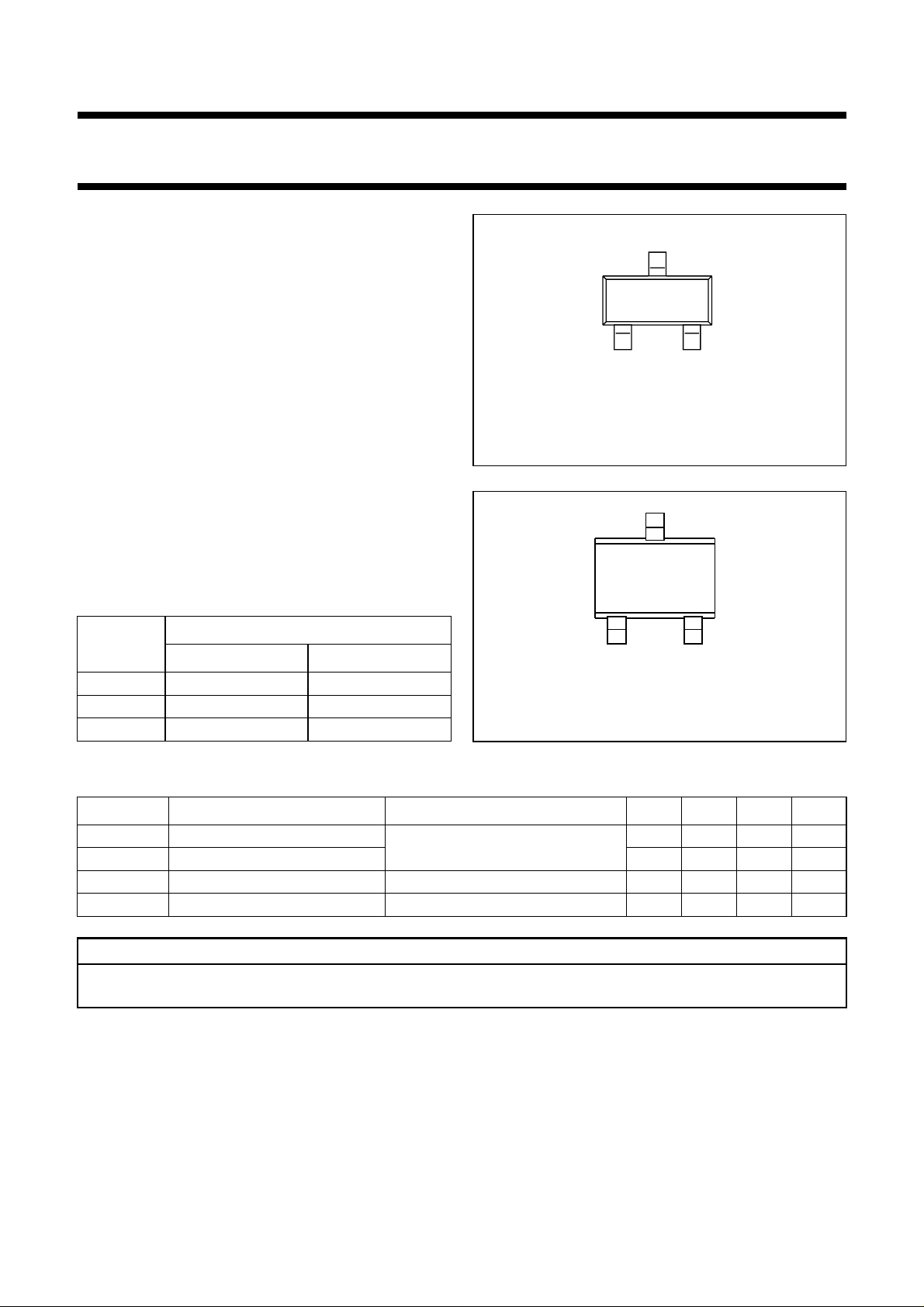
PINNING
DESCRIPTION
PIN
BF1107 BF1107W
1 drain drain
2 source source
3 gate gate
handbook, halfpage
12
Top view
Marking code: S3p.
3
MSB003
Fig.1 Simplified outline SOT23 (BF1107).
handbook, halfpage
Top view
Marking code: W3.
3
1
2
Fig.2 Simplified outline SOT323 (BF1107W).
3
1
2
MAM062
QUICK REFERENCE DATA
SYMBOL PARAMETER CONDITIONS MIN. TYP. MAX. UNIT
21(on)
21(off)
2
losses (on-state) RS=RL=50Ω; f = 50 to 860 MHz −−2.5 dB
2
isolation (off-state) 30 −−dB
drain-source on-resistance VGS= 0; ID=1mA − 12 20 Ω
pinch-off voltage ID=20µA; VDS=1V −−3−4.5 V
S
S
R
V
DSon
GSoff
CAUTION
This product is supplied in anti-static packing to prevent damage caused by electrostatic discharge during transport
and handling. For further information, refer to Philips specs.: SNW-EQ-608, SNW-FQ-302A and SNW-FQ-302B.
1999 May 14 2

Philips Semiconductors Product specification
N-channel single gate MOS-FETs BF1107; BF1107W
LIMITING VALUES
In accordance with the Absolute Maximum Rating System (IEC 134).
SYMBOL PARAMETER MIN. MAX. UNIT
V
DS
V
SD
V
DG
V
SG
I
D
T
stg
T
j
THERMAL CHARACTERISTICS
SYMBOL PARAMETER VALUE UNIT
R
th j-s
drain-source voltage − 3V
source-drain voltage − 3V
drain-gate voltage − 7V
source-gate voltage − 7V
drain current − 10 mA
storage temperature −65 +150 °C
junction temperature − 150 °C
thermal resistance from junction to soldering point; note 1 260 K/W
Note
1. Soldering point of the gate lead.
STATIC CHARACTERISTICS
=25°C unless otherwise specified.
T
j
SYMBOL PARAMETER CONDITIONS MIN. TYP. MAX. UNIT
V
(BR)GSS
V
GSoff
I
DSX
I
GSS
gate-source breakdown voltage VDS= 0; IGS= 0.1 mA 7 −−V
gate-source pinch-off voltage VDS=1V; ID=20µA −−3−4.5 V
drain-source leakage current VGS= −5 V; VDS=2V −−10 µA
gate cut-off current VGS= −5 V; VDS=0 −−100 nA
DYNAMIC CHARACTERISTICS
Common gate; T
amb
=25°C.
SYMBOL PARAMETER CONDITIONS MIN. TYP. MAX. UNIT
S
2losses (on-state) VSG=VDG= 0; RS=RL=50Ω;
21(on)
−−2.5 dB
f = 50 to 860 MHz
V
SG=VDG
= 0; RS=RL=75Ω;
−−3.5 dB
f = 50 to 860 MHz
S
2isolation (off-state) VSG=VDG=5V; RS=RL=50Ω;
21(off)
30 −−dB
f = 50 to 860 MHz
V
SG=VDG
=5V; RS=RL=75Ω;
30 −−dB
f = 50 to 860 MHz
R
C
C
DSon
ig
og
drain-source on-resistance VGS= 0; ID=1mA − 12 20 Ω
input capacitance VSG=VDG= 5 V; f = 1 MHz − 0.9 − pF
V
SG=VDG
= 0; f = 1 MHz − 1.5 2 pF
output capacitance VSG=VDG= 5 V; f = 1 MHz − 0.9 − pF
V
SG=VDG
= 0; f = 1 MHz − 1.5 2 pF
1999 May 14 3
 Loading...