

Philips BF1102, BF1102R Datasheet
DISCRETE SEMICONDUCTORS
DATA SH EET
ook, halfpage
MBD128
BF1102; BF1102R
Dual N-channel dual gate
MOS-FETs
Product specification
Supersedes data of 1999 Jul 01
2000 Apr 11
Philips Semiconductors Product specification
Dual N-channel dual gate MOS-FETs BF1102; BF1102R
FEATURES
• Two low noise gain controlled amplifiers in a single
package
• Specially designed for 5 V applications
• Superior cross-modulation performance during AGC
• High forward transfer admittance
• High forward transfer admittance to input capacitance
ratio.
APPLICATIONS
Gain controlled low noise amplifier for VHF and UHF
applications such as television tuners and professional
communications equipment.
DESCRIPTION
The BF1102 and BF1102R are both two equal dual gate
MOS-FETs which haveashared source pin and a shared
gate 2 pin. Both devices have interconnected source and
substrate; an internal bias circuit enables DC stabilization
and a very good cross-modulation performance at 5 V
supply voltage; integrated diodes between the gates and
source protect against excessive input voltage surges.
Both devices have a SOT363 micro-miniature plastic
package.
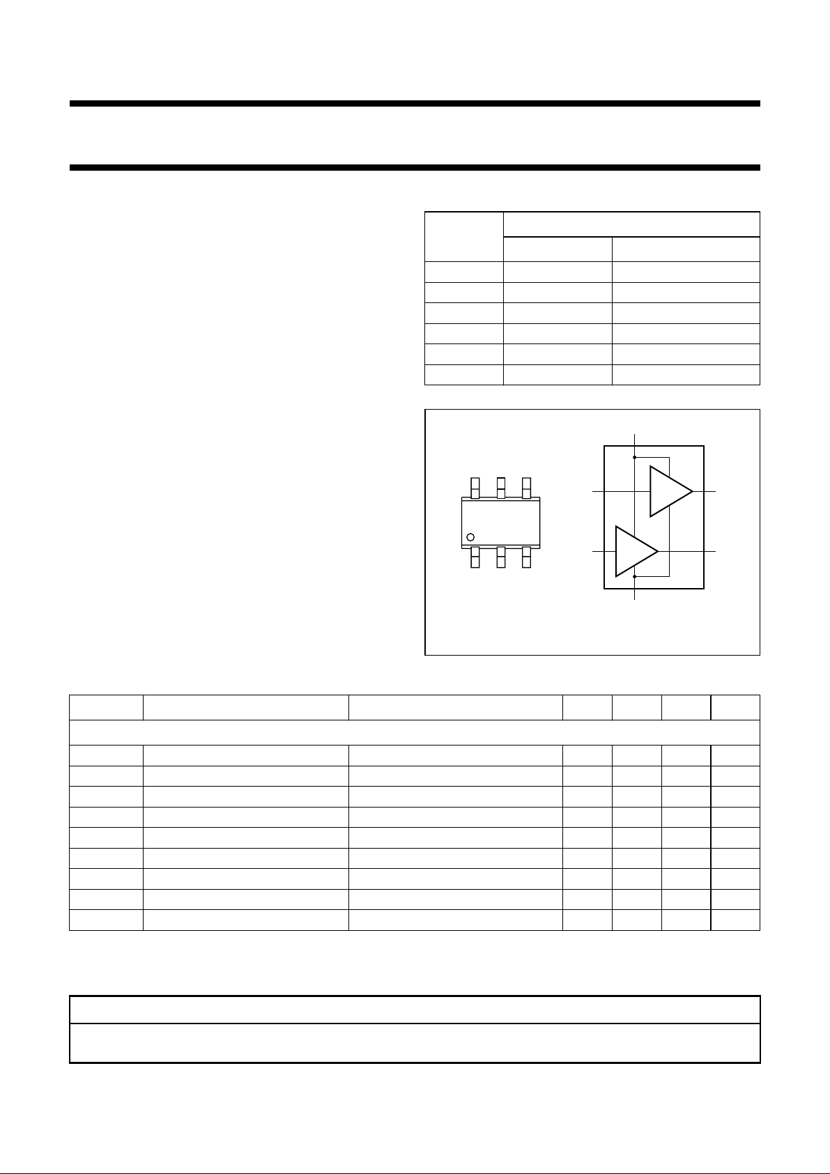
PINNING - SOT363
DESCRIPTION
PIN
BF1102 BF1102R
1 gate 1 (1) gate 1 (1)
2 gate 2 (1 and 2) source (1 and 2)
3 drain (1) drain (1)
4 drain (2) drain (2)
5 source (1 and 2) gate 2 (1 and 2)
6 gate 1 (2) gate 1 (2)
handbook, halfpage
4
56
132
BF1102 marking code: W1.
BF1102R marking code: W2-.
g2 (1, 2)
AMP2
s (1, 2)
Fig.1 Simplified outline and symbol.
AMP1 d (1)g1 (1)
d (2)g1 (2)
MBL029
QUICK REFERENCE DATA
SYMBOL PARAMETER CONDITIONS MIN. TYP. MAX. UNIT
Per MOS-FET unless otherwise specified
V
DS
I
D
P
tot
forward transfer admittance ID=15mA 36 43 − mS
y
fs
C
ig1-s
C
rss
drain-source voltage −−7V
drain current (DC) −−40 mA
total power dissipation Ts≤ 102 °C; note 1 −−200 mW
input capacitance at gate 1 ID=15mA − 2.8 3.6 pF
reverse transfer capacitance f = 1 MHz − 30 50 fF
F noise figure f = 800 MHz − 2 2.8 dB
X
mod
T
j
cross-modulation input level for k = 1% at 40 dB AGC 100 −−dBµV
operating junction temperature −−150 °C
Note
1. T
is the temperature at the soldering point of the source lead.
s
CAUTION
This product is supplied in anti-static packing to prevent damage caused by electrostatic discharge during transport
and handling. For further information, refer to Philips specs.: SNW-EQ-608, SNW-FQ-302A and SNW-FQ-302B.
2000 Apr 11 2

Philips Semiconductors Product specification
Dual N-channel dual gate MOS-FETs BF1102; BF1102R
LIMITING VALUES
In accordance with the Absolute Maximum Rating System (IEC 60134).
SYMBOL PARAMETER CONDITIONS MIN. MAX. UNIT
Per MOS-FET unless otherwise specified
V
DS
I
D
I
G1
I
G2
P
tot
T
stg
T
j
THERMAL CHARACTERISTICS
SYMBOL PARAMETER VALUE UNIT
R
th j-s
drain-source voltage − 7V
drain current (DC) − 40 mA
gate 1 current −±10 mA
gate 2 current −±10 mA
total power dissipation Ts≤ 102 °C − 200 mW
storage temperature −65 +150 °C
operating junction temperature − 150 °C
thermal resistance from junction to soldering point 240 K/W
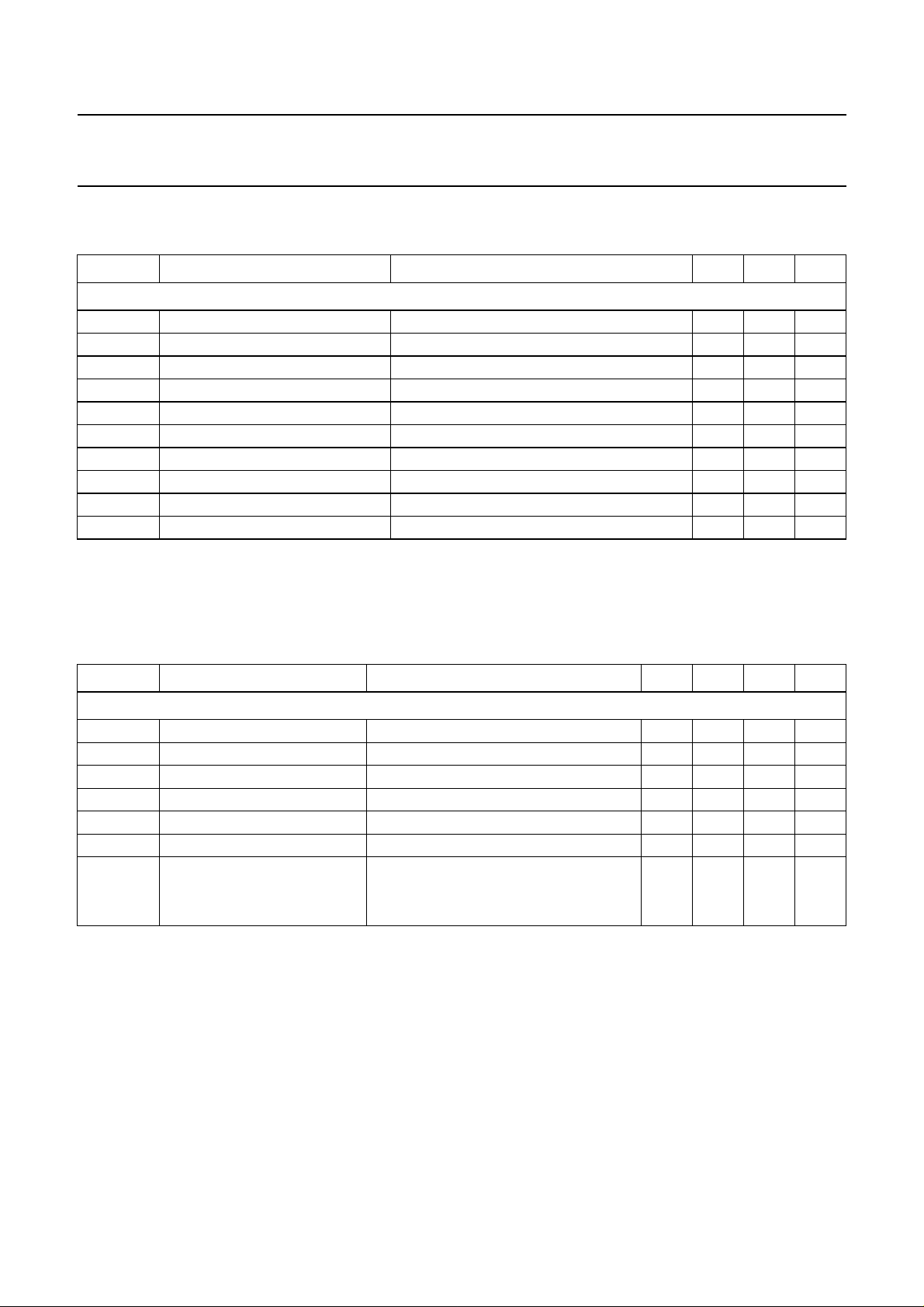
250
handbook, halfpage
P
tot
(mW)
200
150
100
50
0
0 50 100 200
150
Ts (°C)
Fig.2 Power derating curve.
MGS359
2000 Apr 11 3
Philips Semiconductors Product specification
Dual N-channel dual gate MOS-FETs BF1102; BF1102R
STATIC CHARACTERISTICS
Tj=25°C unless otherwise specified.
SYMBOL PARAMETER CONDITIONS MIN. MAX. UNIT
Per MOS-FET unless otherwise specified
V
(BR)DSS
V
(BR)G1-SS
V
(BR)G2-SS
V
(F)S-G1
V
(F)S-G2
V
G1-S(th)
V
G2-S(th)
I
DSX
I
G1-S
I
G2-S
drain-source breakdown voltage V
gate 1-source breakdown voltage VGS=VDS= 0; I
gate 2-source breakdown voltage VGS=VDS= 0; I
forward source-gate 1 voltage V
forward source-gate 2 voltage V
gate 1-source threshold voltage VDS=5V; V
gate 2-source threshold voltage VDS=5V; V
drain-source current V
gate 1 cut-off current V
gate 2 cut-off current V
G1-S=VG2-S
G2-S=VDS
G1-S=VDS
=4V; VDS=5V; RG= 120 kΩ; note 1 12 20 mA
G2-S
=5V; V
G1-S
=5V; V
G2-S
= 0; ID=10µA7−V
=10mA 6 15 V
G1-S
=5mA 6 15 V
G2-S
= 0; I
= 0; I
G2-S
G1-S
G2-S=VDS
G1-S=VDS
= 10 mA 0.5 1.5 V
S-G1
= 10 mA 0.5 1.5 V
S-G2
=4V; ID= 100 µA 0.3 1 V
=4V; ID= 100 µA 0.3 1.2 V
=0 − 50 nA
=0 − 20 nA
Note
1. R
connects gate 1 to VGG=5V.
G1
DYNAMIC CHARACTERISTICS
Common source; T
=25°C; V
amb
=4V; VDS=5V; ID= 15 mA; unless otherwise specified.
G2-S
SYMBOL PARAMETER CONDITIONS MIN. TYP. MAX. UNIT
Per MOS-FET unless otherwise specified (note 1)
forward transfer admittance Tj=25°C 364350mS
y
fs
C
ig1-ss
C
ig2-ss
C
oss
C
rss
F noise figure f = 800 MHz; Y
X
mod
input capacitance at gate 1 f = 1 MHz 2 2.8 3.6 pF
input capacitance at gate 2 f = 1 MHz; (note 2) −−7pF
output capacitance f = 1 MHz − 1.6 2.5 pF
reverse transfer capacitance f = 1 MHz − 30 50 fF
− 2 2.8 dB
cross-modulation fw= 50 MHz; f
S=YS opt
= 60 MHz; (note 3)
unw
input level for k = 1% at 0 dB AGC 85 −−dBµV
input level for k = 1% at 40 dB AGC 100 −−dBµV
Notes
1. Not used MOS-FET: V
= 0; VDS=0.
G1-S
2. Gate 2 capacitance of both MOS-FETs.
3. Measured in test circuit of Fig.20.
2000 Apr 11 4
Philips Semiconductors Product specification
Dual N-channel dual gate MOS-FETs BF1102; BF1102R
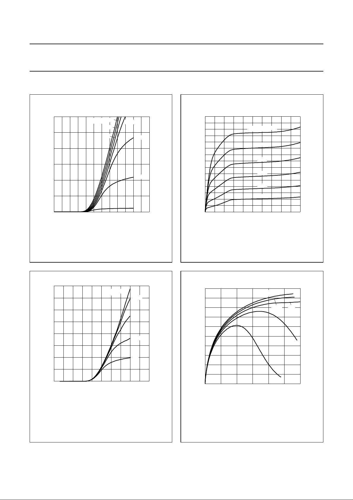
ALL GRAPHS FOR ONE MOS-FET
30
handbook, halfpage
I
D
(mA)
20
10
0
0
VDS=5V.
Tj=25°C.
V
G2-S
0.80.4 2.42.01.61.2
= 4 V
3.5 V
3 V
V
Fig.3 Transfer characteristics; typical values.
160
handbook, halfpage
I
G1
(µA)
120
V
G2-S
= 4 V
2.5 V
G1-S
2 V
1.5 V
1 V
3.5 V
3 V
MGS360
(V)
MGS362
30
handbook, halfpage
I
D
(mA)
20
10
0
010
V
=4V.
G2-S
Tj=25°C.
2468
V
G1-S
= 1.5 V
1.4 V
1.3 V
1.2 V
1.1 V
1 V
Fig.4 Output characteristics; typical values.
50
handbook, halfpage
|yfs|
(mS)
40
V
G2-S
= 4 V
3.5 V
MGS361
VDS (V)
MGS363
3 V
80
40
0
0
VDS=5V.
Tj=25°C.
0.5 2.5
1 1.5 2
2.5 V
2 V
V
G1-S
(V)
Fig.5 Gate 1 current as a function of gate 1
voltage; typical values.
2000 Apr 11 5
30
20
10
0
010 30
VDS=5V.
Tj=25°C.
20
2.5 V
2 V
ID (mA)
Fig.6 Forward transfer admittance as a function
of drain current; typical values.
 Loading...