

Page 1

Colour Television Chassis
QCS1.0S
LA
H_17540_000.eps
140108
Contents Page Contents Page
1. Technical Specifications, Connections, and Chassis
Overview 2
2. Safety Instructions, Warnings, and Notes 5
3. Directions for Use 6
4. Mechanical Instructions 7
5. Service Modes, Error Codes, and Fault Finding 14
6. Block Diagrams, Test Point Overview, and
Waveforms
Wiring Diagram 19
Block Diagram 20
7. Circuit Diagrams and PWB Layouts Diagram PWB
Scaler Board: Power [S-A01] 21 37
Scaler Board: HDMI Input [S-A02] 22 37
Scaler Board: HDMI Switch [S-A03] 23 37
Scaler Board: Analog Input [S-A04] 24 37
Scaler Board: Analog Switch & Output [S-A05] 25 37
Scaler Board: Scaler [S-A06] 26 37
Scaler Board: DDR-SDRAM [S-A07] 27 37
Scaler Board: MCU [S-A08] 28 37
Scaler Board: Fan Control-RTC [S-A08] 29 37
Scaler Board: Panel Interface [S-A09] 30 37
Scaler Board: Audio Amplifier [S-A10] 31 37
Scaler Board: Board Diagram [S-A11] 32 37
Scaler Board: Audio Input [S-A12] 33 37
Scaler Board: Video Decoder [S-A13] 34 37
Scaler Board: Video Decoder SDRAM [S-A14] 35 37
Scaler Board: RS232 [S-A15] 36 37
Keyboard Panel [B] 38 38
IR & LED Panel [L] 39 39
Power Board [P] 40 n.a.
Speaker Board [SP] 41 41
8. Alignments 43
9. Circuit Descriptions, Abbreviation List, and IC Data
Sheets 46
10. Spare Parts List 50
11. Revision List 51
©
Copyright 2008 Philips Consumer Electronics B.V. Eindhoven, The Netherlands.
All rights reserved. No part of this publication may be reproduced, stored in a
retrieval system or transmitted, in any form or by any means, electronic,
mechanical, photocopying, or otherwise without the prior permission of Philips.
Published by JH 0862 BU CD Consumer Care Printed in the Netherlands Subject to modification EN 3122 785 17540
Page 2

EN 2 QCS1.0S LA1.
Technical Specifications, Connections, and Chassis Overview
1. Technical Specifications, Connections, and Chassis Overview
Index of this chapter:
1.1 Technical Specifications
1.2 Connection Overview
1.3 Chassis Overview
Notes:
• Data below can deviate slightly from the actual situation,
due to the different set executions
• Specifications are indicative (subject to change).
1.1 Technical Specifications
1.1.1 Vision
Display type : LCP Display Panel
Screen size : 46" (117 cm), 16:9
Resolution (H × V pixels) : 1920 (× 3) × 1080
Typ. contrast ratio : 1500:1
Min. light output (cd/m
Display colours : 16.7 Million
Viewing angle (H / V degrees) : 176 / 176 degree
Connectivity : VGA-in
Supported video formats : 480i/p
Supported computer formats : 640 × 480 @ 60, 72,
2
) : 450
: VGA-out
:2× HDMI
: Component (YPbPr)
:2× Composite CVBS
: Composite CVBS-out
: S-video
: 3.5 mm audio in
: Audio L/R out
: L/R Speaker-out
: RS232-in
: RS232-out
: 576i
: 720p
: 1080i
: 720 × 400 @ 70 Hz
: 800 × 600 @ 60 Hz
: 1024 × 768 @ 60 Hz
: 1280 × 720 @ 60 Hz
: 1280 × 768 @ 60 Hz
: 1280 × 1024 @ 60 Hz
: 1360 × 768 @ 60 Hz
: 1600 × 1200 @ 60 Hz
: 1920 × 1080 @ 50,
75 Hz
60 Hz
1.1.3 Miscellaneous
Power supply:
- Mains voltage (V
- Mains frequency (Hz) : 50/60 Hz
Ambient conditions:
- Temperature range (°C) : +5 to +40
- Maximum humidity : 80% R.H.
Power consumption (values are indicative)
- Normal operation (W) : ≈ 285
- Stand-by (W) : <5
Dimensions (W × H × D in mm) : 1122 × 663 × 136
Weight (kg) : 32.6
Weight incl. packaging (kg) : 40.2
) : 100 - 240
AC
1.1.2 Sound
Sound systems : Mono
Maximum power (W
):2 × 7 @ 8 Ohm
RMS
:Stereo
Page 3
Technical Specifications, Connections, and Chassis Overview
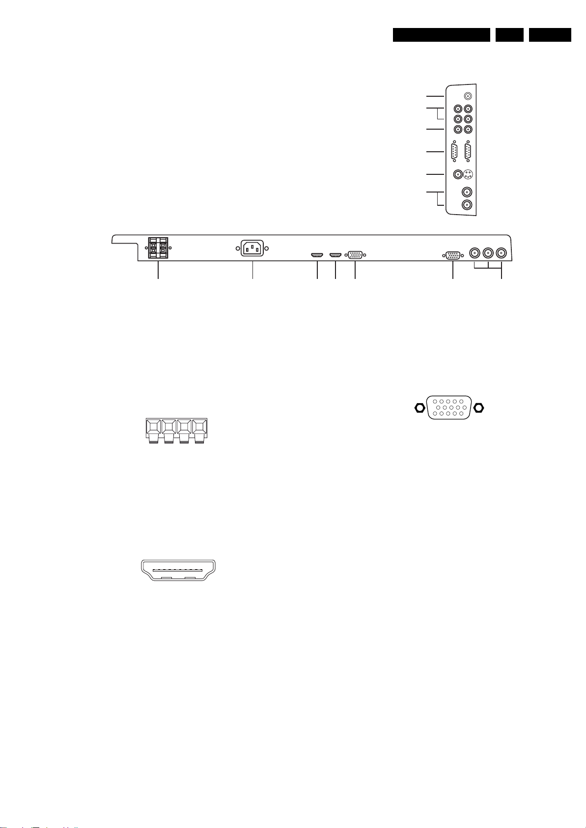
1.2 Connection Overview
EN 3QCS1.0S LA 1.
AUDIO IN 1
AUDIO IN 2, 3
AUDIO OUT
SPEAKER CONNECTIONS POWER SUPPLY RGB 1
Note: The following connector colour abbreviations are used
(acc. to DIN/IEC 757): Bk= Black, Bu= Blue, Gn= Green, Gy=
Grey, Rd= Red, Wh= White, and Ye= Yellow.
1.2.1 Rear Connections
Spring Clip Speaker Connections: Audio - Out
EXTERNAL CONTROL RS-232
COMPOSITE VIDEO IN
COMPOSITE VIDEO BNC
RGB 2
HDMI
RGB 3
VGA
HDMI
Figure 1-1 Rear and Side I/O connections
18 - +5V j
19 - HPD Hot Plug Detect j
20 - Ground Gnd H
VGA RGB 3 & RGB OUT: Video RGB - In, Out
(OUT)
1
6
11
RGB OUT
VGA
E_06532_002.eps
5
10
15
050404
(IN)
(IN)
(OUT)
DVD/HD IN
YPbPr
I_17540_002.eps
280108
E_06532_045.eps
021107
Figure 1-2 Spring Clip Speaker Terminals
Bk - Speaker Left Gnd H
Rd - Speaker Left 7 W / 8 ohm j
Bk - Speaker Right Gnd H
Rd - Speaker Right 7 W / 8 ohm j
HDMI RGB 1 & 2: Digital Video, Digital Audio - In
19
18 2
1
E_06532_017.eps
250505
Figure 1-3 HDMI (type A) connector
1 -D2+ Data channel j
2 -Shield Gnd H
3 -D2- Data channel j
4 -D1+ Data channel j
5 -Shield Gnd H
6 -D1- Data channel j
7 -D0+ Data channel j
8 -Shield Gnd H
9 -D0- Data channel j
10 - CLK+ Data channel j
11 - Shield Gnd H
12 - CLK- Data channel j
13 - n.c.
14 - n.c.
15 - DDC_SCL DDC clock j
16 - DDC_SDA DDC data jk
17 - Ground Gnd H
Figure 1-4 VGA Connector
1 -Video Red 0.7 V
2 -Video Green 0.7 V
3 -Video Blue 0.7 V
/ 75 ohm jk
PP
/ 75 ohm jk
PP
/ 75 ohm jk
PP
4-n.c.
5 -Ground Gnd H
6 -Ground Red Gnd H
7 -Ground Green Gnd H
8 -Ground Blue Gnd H
9-+5V
+5 V jk
DC
10 - Ground Sync Gnd H
11 - n.c.
12 - DDC_SDA DDC data jk
13 - H-sync 0 - 5 V jk
14 - V-sync 0 - 5 V jk
15 - DDC_SCL DDC clock jk
DVD/HD IN: Cinch Video YPbPr - In, Audio - In
Gn - Video Green/Y 0.7 V
Bu -Video Blue/Pb 0.7 V
Rd - Video Red/Pr 0.7 V
/ 75 ohm jq
PP
/ 75 ohm jq
PP
/ 75 ohm jq
PP
1.2.2 Side Connections
Mini Jack: Audio IN1 - In
Wh - Audio L 0.5 V
Rd - Audio R 0.5 V
/ 10 kohm jq
RMS
/ 10 kohm jq
RMS
Cinch: Audio IN 2 & 3 - In
Wh - Audio L 0.5 V
Rd - Audio R 0.5 V
/ 10 kohm jq
RMS
/ 10 kohm jq
RMS
Page 4
EN 4 QCS1.0S LA1.
Technical Specifications, Connections, and Chassis Overview
Cinch: Audio - Out
Rd - Audio - R 0.5 V
Wh - Audio - L 0.5 V
/ 10 kohm kq
RMS
/ 10 kohm kq
RMS
External Control Connector (RS232-UART) Out - In
1
6
5
9
E_06532_005.eps
050404
Figure 1-5 9-pin Sub-D Connector
1 -DCD Carrier Detect j
2 -RxD Receive j
3 -TxD Transmit k
4 -DTR Data Terminal Ready k
5 -Gnd Ground H
6 -DSR Data Set Ready j
7 -RTS Request To Send k
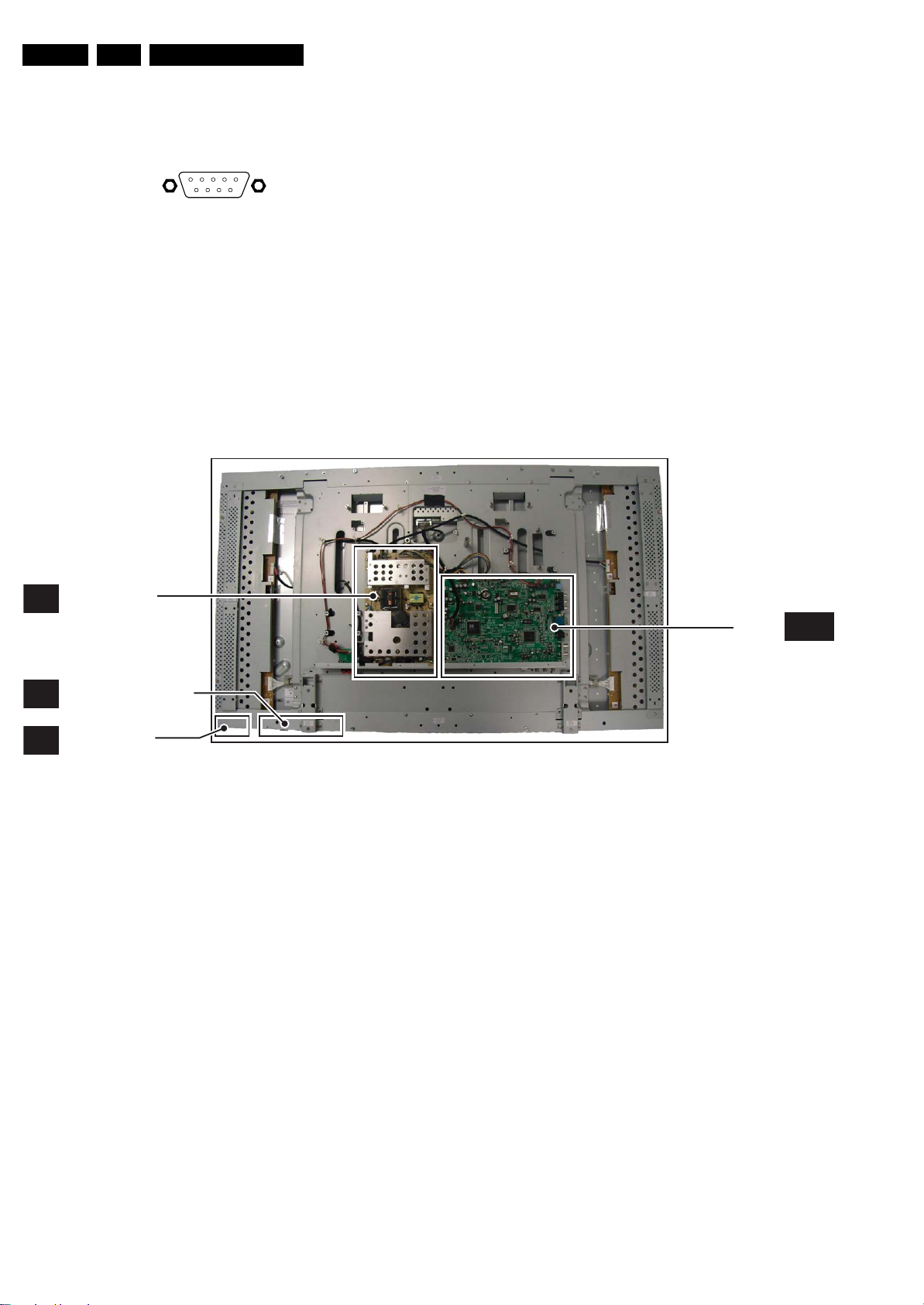
1.3 Chassis Overview
8 -CTS Clear To Send j
9 -RI Ring Indicator j
Cinch: Composite Video CVBS - In
Ye -Video CVBS 1 V
/ 75 ohm jq
PP
S-Video (Hosiden): Composite Video Y/C - In
1 -Ground Y Gnd H
2 -Ground C Gnd H
3 - Video Y 1 V
4 - Video C 0.3 V
/ 75 ohm j
PP
P / 75 ohm j
PP
BNC: Composite Video CVBS - In
Ye -Video CVBS 1 V
/ 75 ohm jq
PP
BNC: Composite Video CVBS - Out
Ye -Video CVBS 1 V
/ 75 ohm kq
PP
POWER BOARD
P
KEYBOARD & CONTROL
B
PANEL
IR & LED PANEL
L
Figure 1-6 PWB/CBA locations
I_17540_047.eps
310108
SCALER
BOARD
S-A
Page 5

Safety Instructions, Warnings, and Notes
2. Safety Instructions, Warnings, and Notes
EN 5QCS1.0S LA 2.
Index of this chapter:
2.1 Safety Instructions
2.2 Warnings
2.3 Notes
2.1 Safety Instructions
Safety regulations require the following during a repair:
• Connect the set to the Mains/AC Power via an isolation
transformer (> 800 VA).
• Replace safety components, indicated by the symbol h,
only by components identical to the original ones. Any
other component substitution (other than original type) may
increase risk of fire or electrical shock hazard.
Safety regulations require that after a repair, the set must be
returned in its original condition. Pay in particular attention to
the following points:
• Route the wire trees correctly and fix them with the
mounted cable clamps.
• Check the insulation of the Mains/AC Power lead for
external damage.
• Check the strain relief of the Mains/AC Power cord for
proper function.
• Check the electrical DC resistance between the Mains/AC
Power plug and the secondary side (only for sets that have
a Mains/AC Power isolated power supply):
1. Unplug the Mains/AC Power cord and connect a wire
between the two pins of the Mains/AC Power plug.
2. Set the Mains/AC Power switch to the “on” position
(keep the Mains/AC Power cord unplugged!).
3. Measure the resistance value between the pins of the
Mains/AC Power plug and the metal shielding of the
tuner or the aerial connection on the set. The reading
should be between 4.5 Mohm and 12 Mohm.
4. Switch “off” the set, and remove the wire between the
two pins of the Mains/AC Power plug.
• Check the cabinet for defects, to prevent touching of any
inner parts by the customer.
2.2 Warnings
• Where necessary, measure the waveforms and voltages
with (D) and without (E) aerial signal. Measure the
voltages in the power supply section both in normal
operation (G) and in stand-by (F). These values are
indicated by means of the appropriate symbols.
2.3.2 Schematic Notes
• All resistor values are in ohms, and the value multiplier is
often used to indicate the decimal point location (e.g. 2K2
indicates 2.2 kohm).
• Resistor values with no multiplier may be indicated with
either an “E” or an “R” (e.g. 220E or 220R indicates 220
ohm).
• All capacitor values are given in micro-farads (μ = × 10
nano-farads (n = × 10
• Capacitor values may also use the value multiplier as the
decimal point indication (e.g. 2p2 indicates 2.2 pF).
• An “asterisk” (*) indicates component usage varies. Refer
to the diversity tables for the correct values.
• The correct component values are listed in the Spare Parts
List. Therefore, always check this list when there is any
doubt.
2.3.3 BGA (Ball Grid Array) ICs
Introduction
For more information on how to handle BGA devices, visit this
URL: www.atyourservice.ce.philips.com (needs subscription,
not available for all regions). After log-in, select “Magazine”,
then go to “Repair downloads”. Here you will find Information
on how to deal with BGA-ICs.
BGA Temperature Profiles
For BGA-ICs, you must use the correct temperature-profile,
which is coupled to the 12NC. For an overview of these profiles,
visit the website www.atyourservice.ce.philips.com (needs
subscription, but is not available for all regions)
You will find this and more technical information within the
“Magazine”, chapter “Repair downloads”.
For additional questions please contact your local repair help
desk.
-9
), or pico-farads (p = × 10
-12
-6
),
).
• All ICs and many other semiconductors are susceptible to
electrostatic discharges (ESD w). Careless handling
during repair can reduce life drastically. Make sure that,
during repair, you are connected with the same potential as
the mass of the set by a wristband with resistance. Keep
components and tools also at this same potential.
• Be careful during measurements in the high voltage
section.
• Never replace modules or other components while the unit
is switched “on”.
• When you align the set, use plastic rather than metal tools.
This will prevent any short circuits and the danger of a
circuit becoming unstable.
2.3 Notes
2.3.1 General
• Measure the voltages and waveforms with regard to the
chassis (= tuner) ground (H), or hot ground (I), depending
on the tested area of circuitry. The voltages and waveforms
shown in the diagrams are indicative. Measure them in the
Service Default Mode (see chapter 5) with a colour bar
signal and stereo sound (L: 3 kHz, R: 1 kHz unless stated
otherwise) and picture carrier at 475.25 MHz for PAL, or
61.25 MHz for NTSC (channel 3).
2.3.4 Lead-free Soldering
Due to lead-free technology some rules have to be respected
by the workshop during a repair:
• Use only lead-free soldering tin Philips SAC305 with order
code 0622 149 00106. If lead-free solder paste is required,
please contact the manufacturer of your soldering
equipment. In general, use of solder paste within
workshops should be avoided because paste is not easy to
store and to handle.
• Use only adequate solder tools applicable for lead-free
soldering tin. The solder tool must be able:
– To reach a solder-tip temperature of at least 400°C.
– To stabilize the adjusted temperature at the solder-tip.
– To exchange solder-tips for different applications.
• Adjust your solder tool so that a temperature of around
360°C - 380°C is reached and stabilized at the solder joint.
Heating time of the solder-joint should not exceed ~ 4 sec.
Avoid temperatures above 400°C, otherwise wear-out of
tips will increase drastically and flux-fluid will be destroyed.
To avoid wear-out of tips, switch “off” unused equipment or
reduce heat.
• Mix of lead-free soldering tin/parts with leaded soldering
tin/parts is possible but PHILIPS recommends strongly to
avoid mixed regimes. If this cannot be avoided, carefully
clear the solder-joint from old tin and re-solder with new tin.
Page 6
EN 6 QCS1.0S LA3.
2.3.5 Alternative BOM identification
The third digit in the serial number (example:
AG2B0335000001) indicates the number of the alternative
B.O.M. (Bill Of Materials) that has been used for producing the
specific TV set. In general, it is possible that the same TV
model on the market is produced with e.g. two different types
of displays, coming from two different suppliers. This will then
result in sets which have the same CTN (Commercial Type
Number; e.g. 28PW9515/12) but which have a different B.O.M.
number.
By looking at the third digit of the serial number, one can
identify which B.O.M. is used for the TV set he is working with.
If the third digit of the serial number contains the number “1”
(example: AG1B033500001), then the TV set has been
manufactured according to B.O.M. number 1. If the third digit is
a “2” (example: AG2B0335000001), then the set has been
produced according to B.O.M. no. 2. This is important for
ordering the correct spare parts!
For the third digit, the numbers 1...9 and the characters A...Z
can be used, so in total: 9 plus 26= 35 different B.O.M.s can be
indicated by the third digit of the serial number.
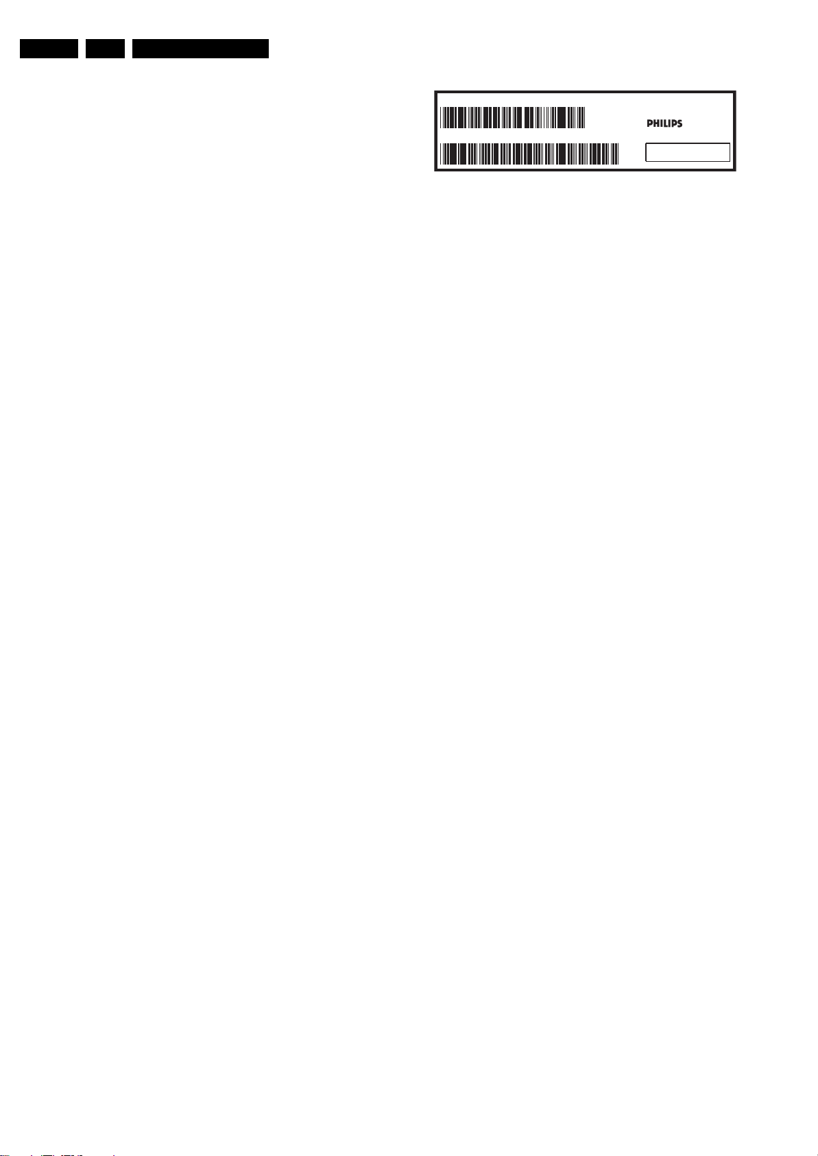
Identification: The bottom line of a type plate gives a 14-digit
serial number. Digits 1 and 2 refer to the production centre (e.g.
AG is Bruges), digit 3 refers to the B.O.M. code, digit 4 refers
to the Service version change code, digits 5 and 6 refer to the
production year, and digits 7 and 8 refer to production week (in
example below it is 2006 week 17). The 6 last digits contain the
serial number.
Directions for Use
MODEL :
PROD.NO:
2.3.6 Board Level Repair (BLR) or Component Level Repair (CLR)
If a board is defective, consult your repair procedure to decide
if the board has to be exchanged or if it should be repaired on
component level.
If your repair procedure says the board should be exchanged
completely, do not solder on the defective board. Otherwise, it
cannot be returned to the O.E.M. supplier for back charging!
2.3.7 Practical Service Precautions
• It makes sense to avoid exposure to electrical shock.
• Always respect voltages. While some may not be
32PF9968/10
AG 1A0617 000001
Figure 2-1 Serial number (example)
While some sources are expected to have a possible
dangerous impact, others of quite high potential are of
limited current and are sometimes held in less regard.
dangerous in themselves, they can cause unexpected
reactions that are best avoided. Before reaching into a
powered TV set, it is best to test the high voltage insulation.
It is easy to do, and is a good service precaution.
MADE IN BELGIUM
220-240V 50/60Hz
VHF+S+H+UHF
S
~
BJ3.0E LA
E_06532_024.eps
128W
130606
3. Directions for Use
You can download this information from the following websites:
http://www.philips.com/support
http://www.p4c.philips.com
Page 7
4. Mechanical Instructions
Mechanical Instructions
EN 7QCS1.0S LA 4.
Index of this chapter:
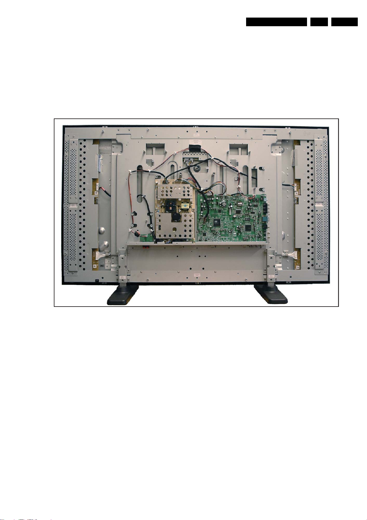
4.1 Cable Dressing
4.2 Service Positions
4.3 Assy/Panel Removal
4.4 Set Re-assembly
4.1 Cable Dressing
Notes:
• Figures below can deviate slightly from the actual situation,
due to the different set executions.
• Follow the disassembly instructions in the described order.
4.2 Service Positions
When moving or laying down an LCD set, at least two people
must work together. Avoid any impact towards the PDP set.
For easy servicing of this set, there are a few possibilities
created:
• Foam bars (created for Service).
• Separately available stands.
4.2.1 Foam Bars
The foam bars (order code 3122 785 90580 for two pieces) can
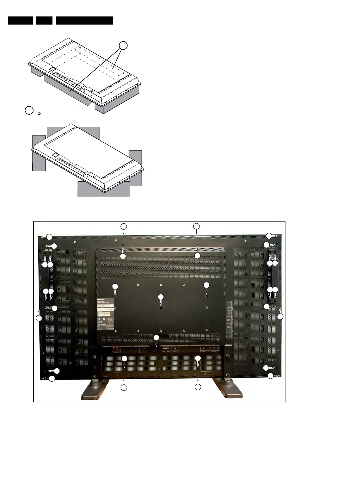
be used for all types and sizes of Flat TVs. See figure “Foam
bars” for details. Sets with a display of 42" and larger, require
four foam bars [1]. Ensure that the foam bars are always
supporting the cabinet and never only the display. Caution:
Failure to follow these guidelines can seriously damage the
display!
By laying the TV face down on the (ESD protective) foam bars,
a stable situation is created to perform measurements and
alignments. By placing a mirror under the TV, you can monitor
the screen.
Figure 4-1 Cable dressing
4.2.2 Stands
I_17540_012.eps
280108
For this set separately orderable stands are available, which
can also be used during service.
Page 8
EN 8 QCS1.0S LA4.
Mechanical Instructions
4.3 Assy/Panel Removal
Required for sets
1
42"
1
E_06532_018.eps
171106
4.3.1 Back Cover
Warning: Disconnect the mains power cord before you open
the set.
Figure 4-2 Foam bars
1
1
1
1
1
1
1
11
1
1
1
1
1 1
1
11
1
1
1
1
1
1
1
1
1
1
1
1
1
1
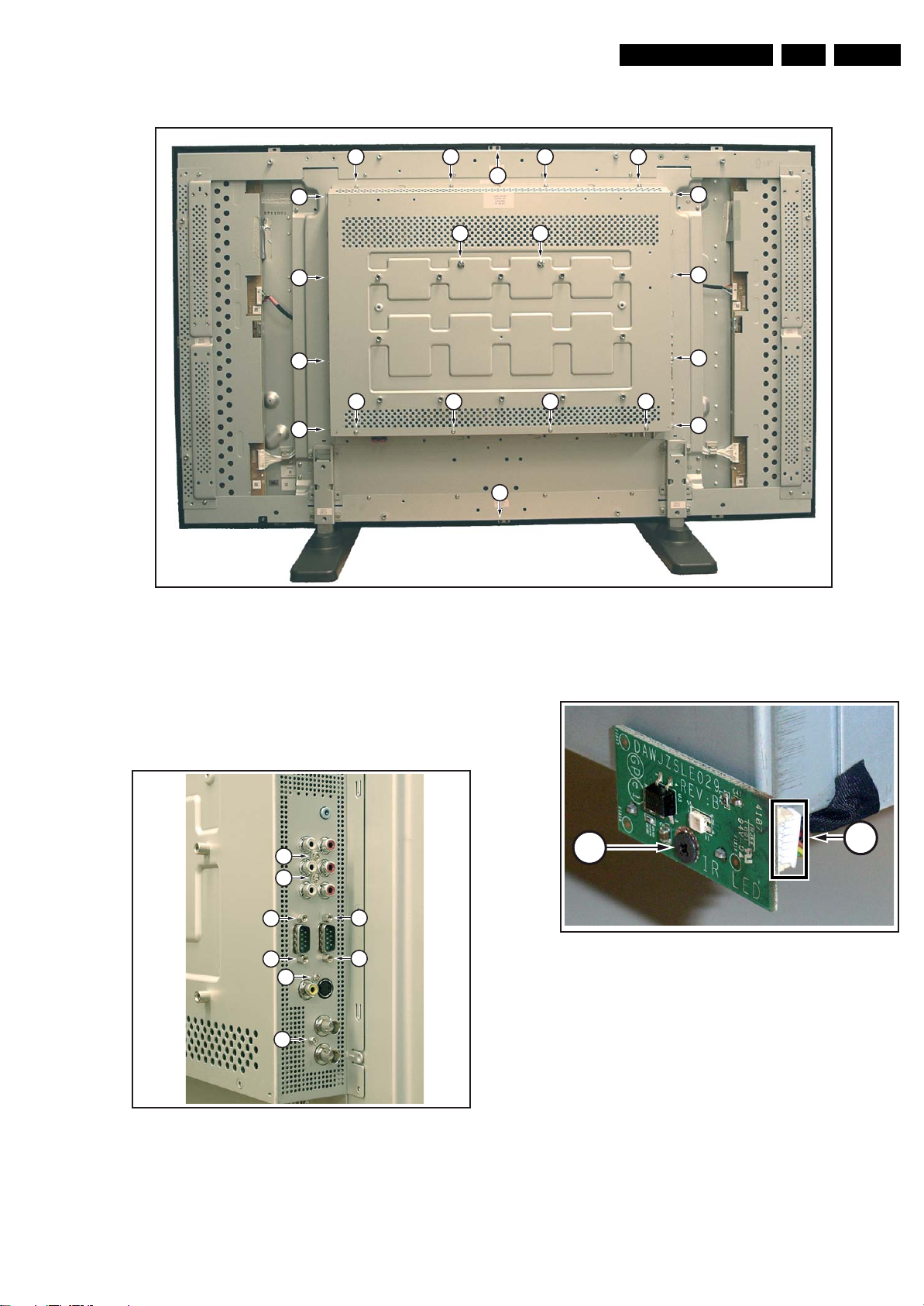
Refer to figure “Back Cover removal” for details.
1. Remove all screws [1] from the back cover.
2. Lift the back cover from the cabinet.
Figure 4-3 Back Cover removal
I_17540_014.eps
280108
Page 9
4.3.2 Front Cover and Shielding
Mechanical Instructions
EN 9QCS1.0S LA 4.
3
333
1
3
3
2 2
3
3
3
3
3 3 3 3
3
3
1
I_17540_013.eps
280108
Figure 4-4 Front Cover and Shielding removal [1/2]
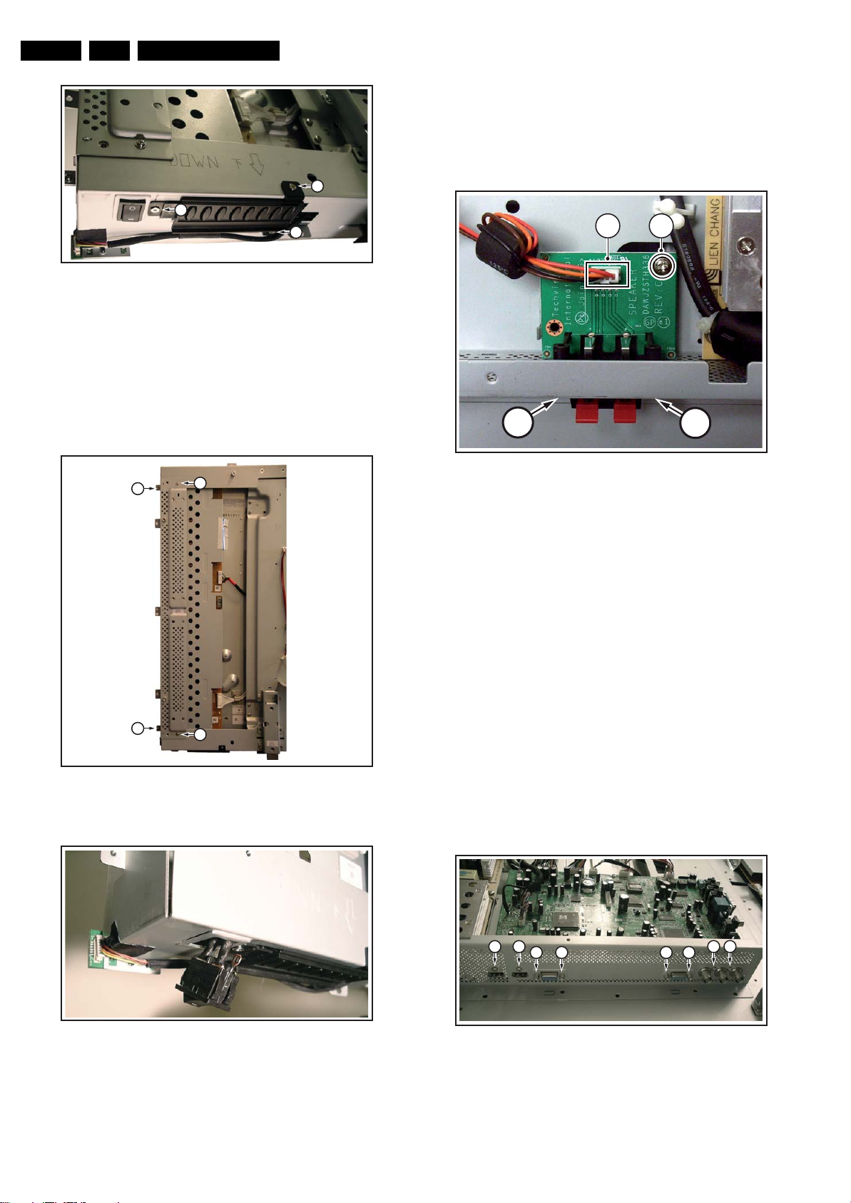
Refer to figure “Front Cover and Shielding removal” for details.
1. Remove screws [1].
2. Lift the front cover from the set.
3. Remove screws [2] and [3] from the shielding.
4. Now gently lift the shielding from the set while pushing it
sidewards, away from the power switch.
2
2
2
2
2
2
2
2
4.3.3 LED / IR Panel
1
Figure 4-6 LED / IR Panel removal
Refer to figure “LED / IR Panel removal” for details.
1. Remove the fixation screw[1].
2. Take out the panel.
3. Disconnect the cable [2] from the rear of the panel.
When defective, replace the whole unit.
2
I_17540_003.eps
280108
Figure 4-5 Front Cover and Shielding removal [2/2]
4.3.4 Keyboard Control Panel
I_17540_011.eps
280108
Page 10
EN 10 QCS1.0S LA4.
1
Figure 4-7 Keyboard Control Panel removal
Refer to figure “Keyboard Control Panel removal” for details.
1. Remove back- and front cover as described earlier.
2. Remove the fixation screws [1].
3. Take out the panel assembly and release the connector.
When defective, replace the whole unit.
Mechanical Instructions
4.3.6 Speaker Panel
1
1
I_17540_006.eps
280108
2. Remove the fixation screws [1] from the rim and remove it.
3. Now the clips that hold the power switch can be released
via the backside of the switch.
When defective, replace the whole unit.
1 2
4.3.5 Power Supply Switch
1
1
Figure 4-8 Power Supply Switch removal [1/2]
2
2
I_17540_004.eps
280108
1
Figure 4-10 Speaker Panel removal
Refer to figure “Speaker Panel removal” for details.
1. Unplug the connector [1] from the speaker panel.
2. Remove the fixation screws [2].
3. Take out the panel.
When defective, replace the whole unit.
4.3.7 Small Signal Panel (SSB)
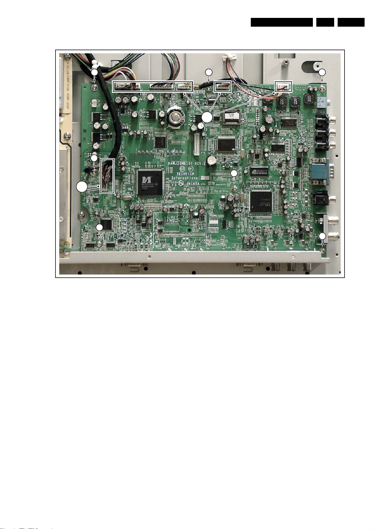
Refer to figures “SSB Connector Plate” and “SSB” for details.
1. Remove the screws [1] securing the connector plate.
2. Do NOT forget to unplug the LVDS connector [2] from the
SSB. Important: Be careful, as this is a very fragile
connector!
3. Remove the ground cable screw [3].
1
4. Unplug the other connectors [4] from the SSB.
5. Remove all fixation screws [5] securing the SSB.
I_17540_005.eps
280108
6. Lift out the SSB.
When defective, replace the whole unit.
Notes:
• Pay special attention to the EMC foam on the SSB
shielding. These must be replaced in their initial positions
during set re-assembly.
I_17540_008.eps
Figure 4-9 Power Supply Switch removal [2/2]
Refer to figure “Power Supply Switch removal” for details.
1. Remove back- and front cover as described earlier.
280108
1 1
1 1 1 1
Figure 4-11 SSB Connector Plate
1 1
I_17540_009.eps
280108
Page 11
Mechanical Instructions
EN 11QCS1.0S LA 4.
5
5 5
4
3
5
2
5
5
Figure 4-12 SSB
I_17540_010.eps
280108
Page 12
EN 12 QCS1.0S LA4.
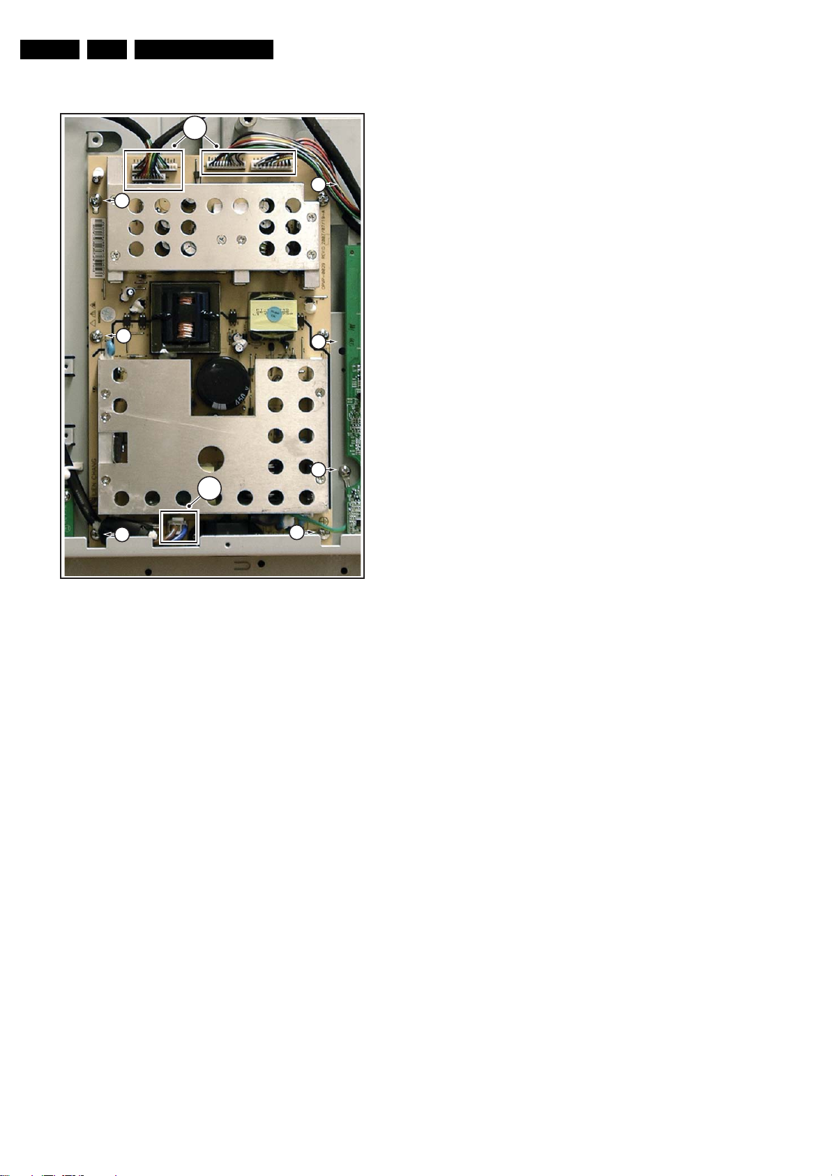
4.3.8 Main Supply Panel
3
Mechanical Instructions
1
3
3
1
3
Figure 4-13 Main supply panel.
1. Refer to figure “Main supply panel”.
2. Unplug connectors [1].
3. Remove the grounding screw [2].
4. Remove the fixation screws [3].
5. Take the board out.
When defective, replace the whole unit.
3
2
3
I_17540_045.eps
310108
Page 13
4.3.9 LCD Panel
Important: Be sure to work in a dust free environment during
the following activities. In addition, the use of (fabric) hand
gloves is advised.
Mechanical Instructions
EN 13QCS1.0S LA 4.
4
4
2
1
3
4
4
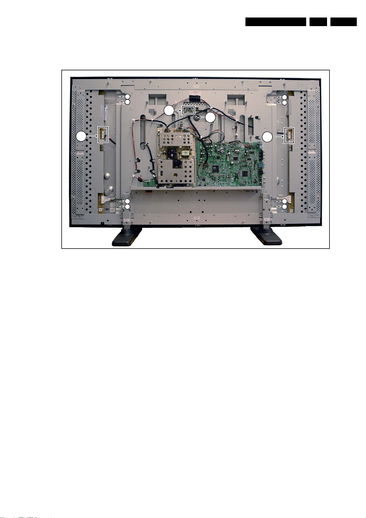
Figure 4-14 Plasma panel disassembly
4
4
3
4
4
I_17540_001.eps
280108
1. First remove front cover, back cover and shielding as
described earlier.
2. Place the TV set face down on the foam bars. Place the
bars at each of the four the edges of the set, so they will
support the front frame and not only the glass plate!
3. Remove the grounding screw [1] that secures the cabling.
4. Do NOT forget to unplug the LVDS connector [2] from the
SSB. Important: Be careful, as this is a very fragile
connector!
5. Unplug the connectors from the backlight inverters [3].
6. Remove the screws [4].
7. Now gently lift the complete subframe from the LCD panel.
When defective, replace the whole unit.
4.4 Set Re-assembly
To re-assemble the whole set, execute all processes in reverse
order.
Notes:
• While re-assembling, make sure that all cables are placed
and connected in their original position. See figure “Cable
dressing”.
• Pay special attention not to damage the EMC foams at the
SSB shields. Make sure, that EMC foams are put correctly
on their places.
Page 14

EN 14 QCS1.0S LA5.
Service Modes, Error Codes, and Fault Finding
5. Service Modes, Error Codes, and Fault Finding
Index of this chapter:
5.1 Compatibility Mode
5.2 Service Mode
5.1 Compatibility Mode
This chassis does not contain specific test points, since all
defect boards should be replaced.
Perform measurements under the following conditions:
• Environmental: t
• Service signal: 100% Full White signal
This monitor saves all previously made settings, unless
separately made user settings override this. All timings must be
properly phased, sized and centred. The aspect ratio is
depending on the input signal scaled and centred. At full screen
the input timing is set to completely fill the screen, regards less
of scaling artifacts.
5.1.1 Overscan
Component over scan: 5~8%
5.1.3 Compatibility
Mode Aspect Ratio Handling
Standard Resolution Full Screen Aspect Ratio Composite SVHS YPbPr RGB HDMI
VESA 640 × 480 @ 60 Hz 1920 × 1 080 16 : 9 No No No Yes Yes
VESA 640 × 480 @ 72 Hz 1920 × 1 080 16 : 9 No No No Yes Yes
VESA 640 × 480 @ 75 Hz 1920 × 1 080 16 : 9 No No No Yes Yes
VESA 800 × 600 @ 60 Hz 1920 × 1 080 16 : 9 No No No Yes Yes
VESA 1024 × 600 @ 60 Hz 1920 × 1 080 16 : 9 No No No Yes Yes
PD40 1280 × 768 @ 60 Hz 1 920 × 1080 16 : 9 No No No Yes Yes
VESA (M9) 1 280 × 768 @ 60 Hz 1920 × 1080 16 : 9 No No No Yes Yes
VESA 1280 × 1024 @ 60 Hz 1920 × 1080 16 : 9 No No No Yes Yes
M9 1360 × 768 @ 60 Hz 1 920 × 1080 16 : 9 No No No Yes Yes
VESA 1360 × 768 @ 60 Hz 1920 × 1 080 16 : 9 No No No Yes Yes
VESA 1600 × 1200 @ 60 Hz 1920 × 1080 16 : 9 No No No Yes Yes
M9 1920 × 1080 @ 50 Hz 1920 × 1080 16 : 9 No No No Yes Yes
SMPTE 1920 × 1080 @ 60 Hz 1920 × 1080 16 : 9 No No No Yes Yes
PAL 576i @ 50 Hz 1 920 × 1080 16 : 9 Yes Yes Yes No Yes
NTSC 480i @ 60 Hz 1920 × 1080 16 : 9 Yes Yes Yes No Yes
DVD 480p @ 60 Hz 1920 × 1080 16 : 9 No No Yes No Yes
= 25 ±2°C, RH = 65 ±10%
env
720 × 400 @ 70 Hz 1920 × 1080 16 : 9 No No No Yes Yes
1280× 720 @ 60 Hz 1920 × 1080 16 : 9 No No No Yes Yes
1920× 1080 @ 60 Hz 1920 × 1080 16 : 9 No No No Yes Yes
720p @ 50 Hz 1920 × 1080 16 : 9 No No Yes No Yes
720p @ 60 Hz 1920 × 1080 16 : 9 No No Yes No Yes
1080i @ 50 Hz 1920 ×
1080i @ 60 Hz 1920 × 1080 16 : 9 No No Yes No Yes
AV over scan: 5~9%
HDMI over scan: No over scan for PC input, 5~9% for video
source.
PC: No over scan
5.1.2 Display Processor performance
The display processor performance (excluding scaling
artifacts) has to be judged according to the following
definitions:
• Compatibility mode: correctly recognizes the proper
resolution and applies the correct display scaling to the
image. (i.e. a 1280 × 720 signal is properly recognized).
• Properly sized/centred: The entire image (use display mate
“side tics” pattern) perfectly fits the screen. Even one pixel
off in horizontal or vertical direction, makes this test fail.
• Properly phased: The display processor automatically
computes the correct A/D response so that a Win98
shutdown or all display mate moire patterns are correctly
displayed. Most critical on the panels native mode, no
unstableness of the image may be observed.
• HD compatibility: All HD timings have to work through
YPbPr, HDMI, and RGB.
1080 16 : 9 No No Yes No Yes
5.2 Service Mode
5.2.1 Factory Mode
There are two ways to enter the factory mode:
1. On the set:
• Push the y button and turn on the AC power.
2. With the remote control:
• Turn on the set and provide a signal source on an input
(this to prevent to enter the power save mode). On the
remote control press “-”, ”-”, “+”, “+”, “-”, “+”, “-”, “+”,
“SET”, “MENU”.
• Please note that this set does not respond on the
standard Philips remote controllers, but only responds
to the with the set supplied remote control.
Figure 5-1 Remote control.
I_17540_007.eps
280108
Page 15
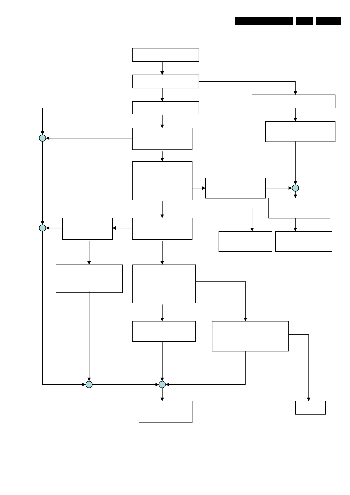
5.2.2 Repair flow chart
Service Modes, Error Codes, and Fault Finding
No Image appear
EN 15QCS1.0S LA 5.
Not OK
Check CN2
pin10 > 2V?
OK
Orange
Not OK
Not OK
LED Bright ?
OK
Check LED status
Green
Check CN7
pin1 > 3.3V?
OK
Check CN7
pin9/20=12V?,
CN2 pin7/8
=24V?
OK
Check LCD
Back Light
OK
Not OK
Check CN2 cable
connection
Replace Power
board
Not OK
Check CN7 pin6 = 5 V?
Not OK
Check cable from
CN7(MB) connection
OK, Well
connection
Check Power
Board AC power
OK
Check P1(PWB)
connection
Not OK
Check cable
connection between
PWB and Panel
OK, Well
connection
Disconnected the
Signal cable, Is
the screen show
“No Signal”?
NG
Check CN1(MB)
cable connection
OK, Well
connection
Replace Main
board
OK
Connected the Signal
cable again,
Check Image
Not OK
OK
END
I_17540_042.eps
310108
Page 16
EN 16 QCS1.0S LA5.
Service Modes, Error Codes, and Fault Finding
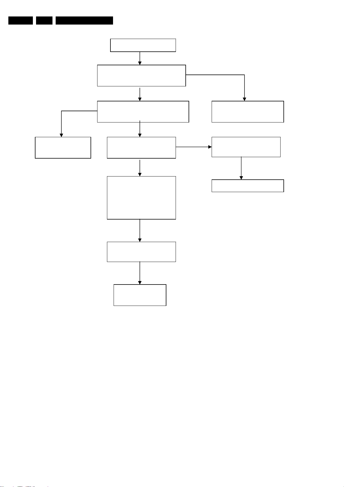
No Audio
Is Audio Input Source
selection correct?
Not OK
Reset mute
and Volume
OK
Is Mute and volume setting
OK?
OK
Check CN2 pin1/2
=12V?
OK
Check connector
connectted between
MB(CN5/CN6) and
CN13(Speaker
Interface)
OK, Well
connection
Check Speaker
Terminal connection
Not OK
Not OK
Select correct Audio
Input Source
Check CN2 cable
connection
OK, Well
connection
Replace Power board
OK, Well
connection
Replace Main
board
I_17540_043.eps
310108
Page 17
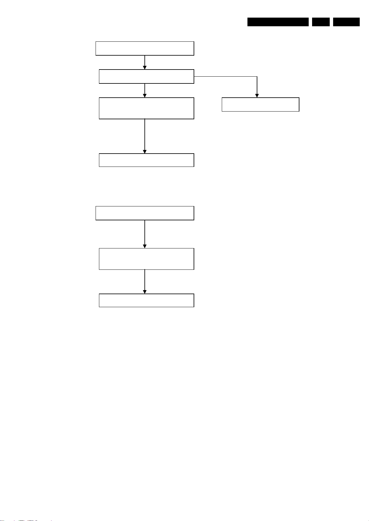
Service Modes, Error Codes, and Fault Finding
Remote No Function
Check Battery
OK
EN 17QCS1.0S LA 5.
Not correct
Check cable from CN14(MB)
connection
OK, Well
connection
Replace IR/LED Board
Button Key No Function
Check cable from CN3(MB)
connection
OK, Well
connection
Change Battery
Replace KEY Board
I_17540_044.eps
310108
Page 18
EN 18 QCS1.0S LA5.
Personal Notes:
Service Modes, Error Codes, and Fault Finding
E_06532_012.eps
131004
Page 19
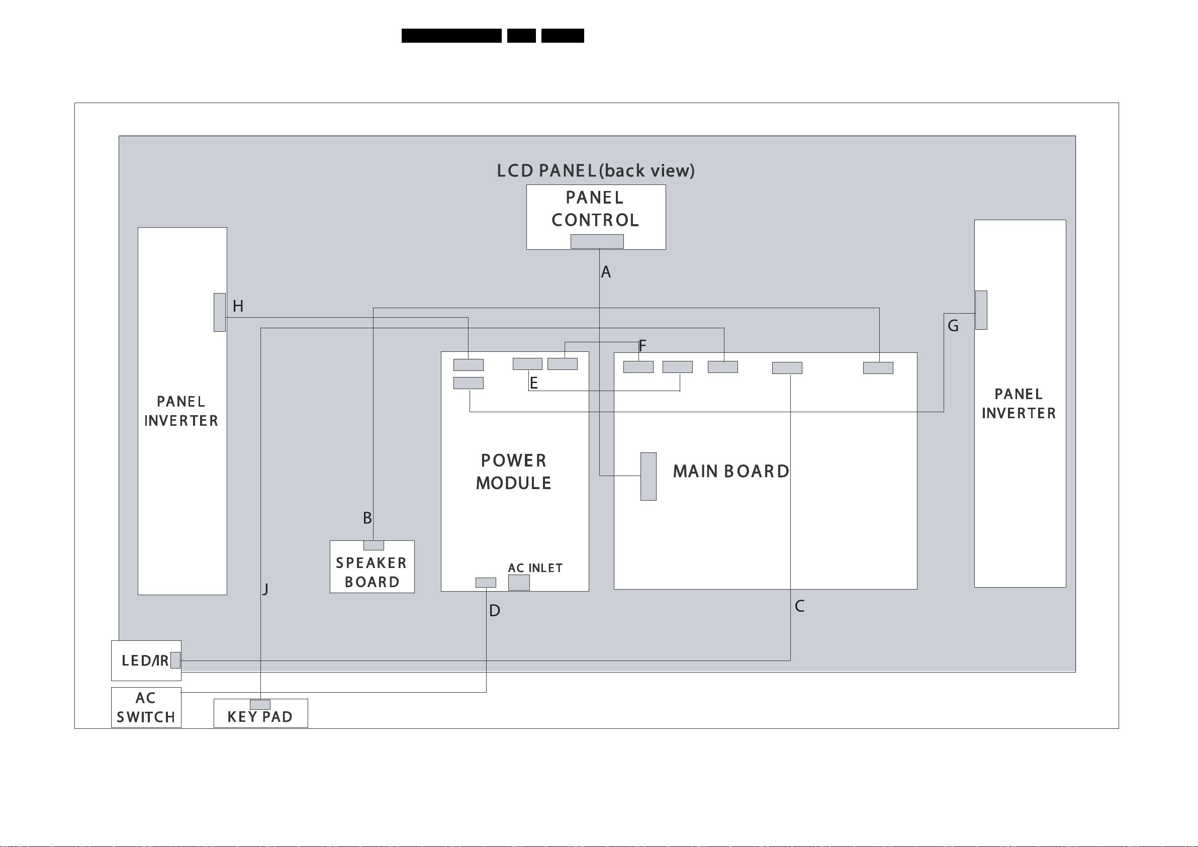
Block Diagrams, Test Point Overview, and Waveforms
6. Block Diagrams, Test Point Overview, and Waveforms
Wiring Diagram
WIRING DIAGRAM
19QCS1.0S LA 6.
I_17540_016.eps
310108
Page 20
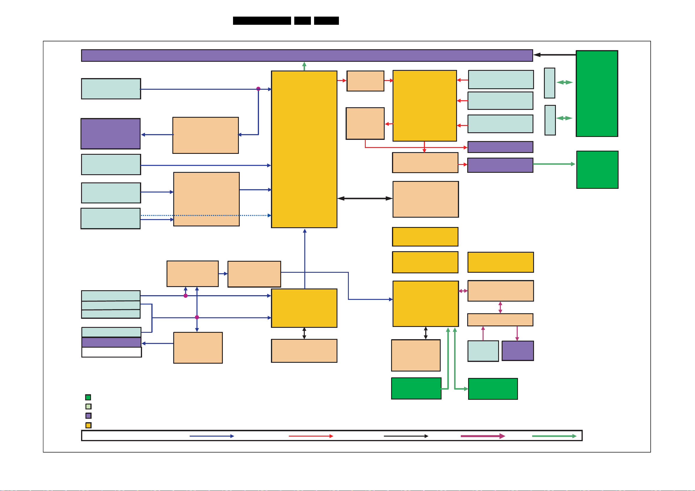
Block Diagrams, Test Point Overview, and Waveforms
Block Diagram
BLOCK DIAGRAM
20QCS1.0S LA 6.
L C D P A N E L(LK460D3LZ18)
D-SUB VGA
(CN6)
D-SUB
VGA Output
(CN9)
BNC (YPbPr)
(CN7)
HDMI1
(CN5)
HDMI2
(CN4)
VIDEO BUFFER
TSH340
(U24/U27/U28)
HDMI SW
TMDS341SA
(U11)
(CN16)
SCALER
5251A
(U29A)
Audio
DAC
Audio
Buffer
TS482ID
AUDIO SW
NJW1411M
AUDIO AMP
YDA138
DDR SDRAM
M13S128324A
RTC
PCF8563
Phone Jack
Audio1 IN
RCA
Audio2 IN
RCA
Audio3 IN
RCA Audio
Output Terminal
C
N
1
C
N
2
Power
Module
Speaker
Board
S-VIDEO
RCA (CVBS)
(Jack1)
BNC (CVBS)
BNC (CVBS)
(J1)
PCBA
Input Port
Output
I2C Device
CSYNC
SELECTOR
PI5V331(U44)
Video Buffer
MM1671
(U42)
SYNC
SEPARATOR
LM1881(U43)
VIDEO
DECODER
UPD64015
SDRAM
IS42S16100
EEPROM
24LC32A
MCU
W79E659
(U34)
FLASH
EN29F040
(U33)
KEYPAD
Board
GPIO
EXPANDER
DUAL 1-4 MUX
PI5C3253
RS-232 SP3243
RS-232
IN
RS-232
OUT
IR/LED
Board
Video SignalAudio SignalDataSignal UART Wiring
I_17540_017.eps
310108
Page 21
Circuit Diagrams and PWB Layouts
7. Circuit Diagrams and PWB Layouts
21QCS1.0S LA 7.
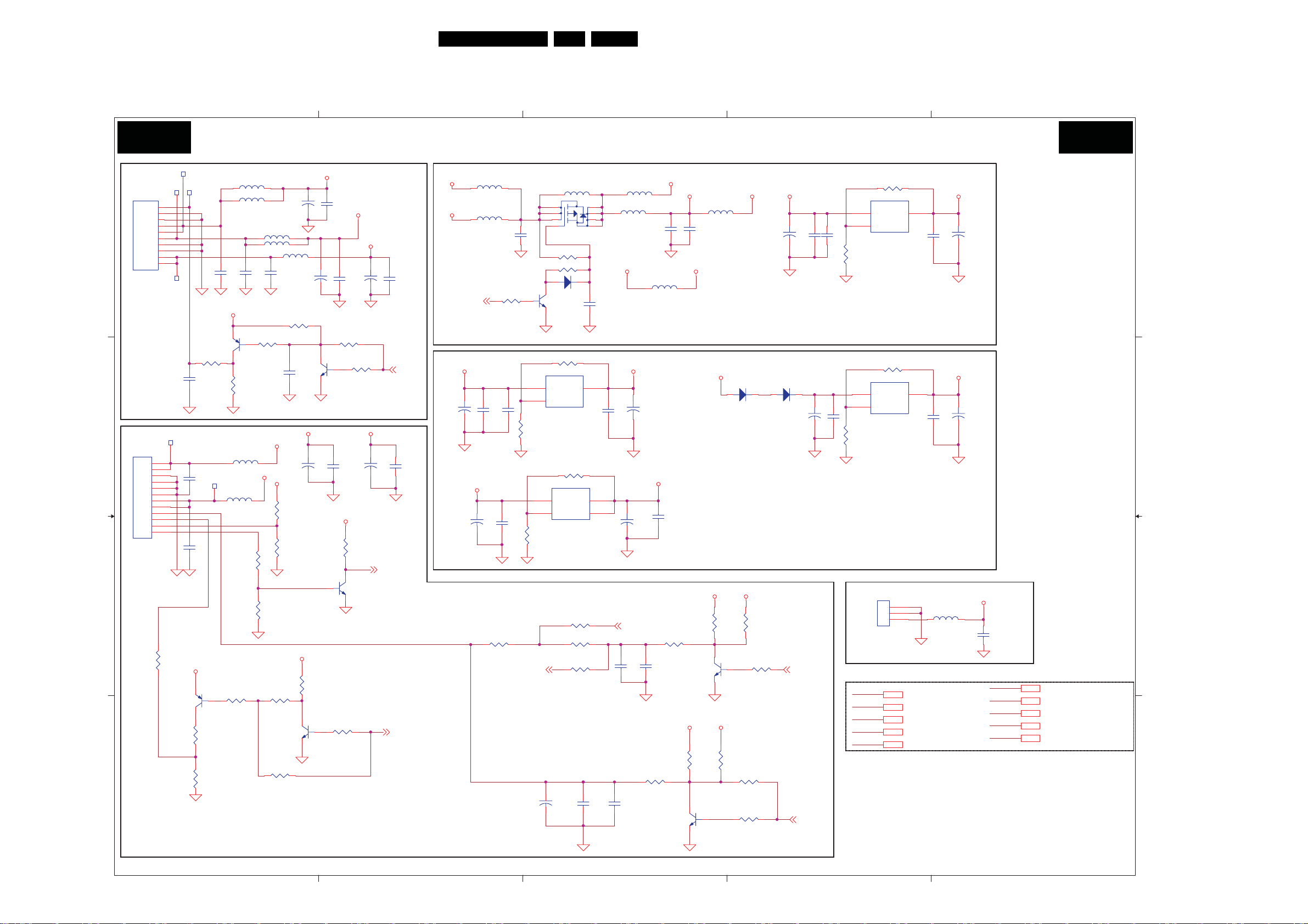
Scaler Board: Power
5
4
3
2
1
SCALER BOARD: POWER
S-A01 S-A01
TP1
TP2
TP3
1
1
2
2
3
3
4
4
5
5
6
6
7
7
D D
C C
EIC_4500-E12N
B B
A A
8
9
10
EIC_4606-10
CN1
CN2
R29
100
8
9
10
TP5
12
11
10
9
8
7
6
5
4
3
2
1
1
2
MMBT3906
TP4
Q7
R648
0R
R30
1K
PS_ON
MMBT3906
1 2
1
C20
NC
2
1
2
C34
1
2
C39
+5V_SW
1
3
1
2
1
2
0.1uF
PWM
0.1uF/NC
L1
KHB0805R121SA
L5
KHB0805R121SA
L9
KHB0805R121SA
L10
1
1
C11
C12
0.1uF
0.1uF
2
2
+5VS
Q3
1
R9
0R
TP6
KHB0805R121SA/NC
BKLT_EN
2
2
3
2
R13
1K
1
L13
KHB0805R121SA
L14
R21
10K
R22
4.7K
R34
10K
12
KHB0805R121SA
L11
KHB0805R121SA
1
C13
0.1uF
2
R6 4.7K/NC
1 2
R7 4.7K
12
1
2
+12VA
+24VA
+3.3AV DD
1
R17
0R/NC
2
1
R19
2
0R
2
1
1
2
+5V_SW
R35
10K/NC
12
R39
0R
12
C1
220uF/35V
C19
NC
+12VA
0
C3
1
2
3
1
1
2
1
2
R33
10K/NC
+5V_SW
1
+
C2
0.1uF
2
1
+
C14
2
220uF/35V
3
2
Q4
1
MMBT3904/NC
1
+
2
220uF/35V
+5V_SW
2
10K/NC
2
Q8
MMBT3904/NC
+5VS
1
C16
0.1uF
2
R8
0R
4.7K/NC
C32
0.1uF
2
1
3
Q5
MMBT3904
1
R36
R11
R20
10K
12
5
C1
12
C31
+12V_SW
1
+
2
12
+24VA
1
+
2
1
C17
0.1uF
2
220uF/35V
STBY
C
1
35V/N
C33
0.1uF/NC
2
220uF/
SELFD_INV
PBIAS
+5VS
+5V_SW
PWR_OFF
C21
470uF/16V
470uF/16V
PWM
L2
KHB0805R121SA
L8
KHB0805R121SA/NC
+5VSB
+
C35
C23
0.1uF
+5VSB
1
2
+
0.1uF
C7
0.1uF
R5
4.7K
1 2
C24
0.1uF
C38
R26
10K/NC
PWM
1
2
MMBT3904
1
2
12
EXT_VBR
C43
10uF/50V
L3
KHB0805R121SA/NC
2
3
4 5
R3 10K
1 2
R4 0R
1 2
D1
1 2
3
NC
2
Q2
1
R10 200/1%
U2
3
VIN
1
ADJ/GND
AIC1084/TO263
R14
330/1%
R16 330/1%
U4
3
VIN
1
ADJ/GND
AP1117ELA/TO223
R18
330/1%
R25 NC
R27 0R
R31NC
1
NC
2
C44
VOUT
VOUT
Q1
SI9435
OUT
81
7
6
1
NC
2
2
2
4
12
12
12
1
2
L4
KHB0805R121SA
L6
KHB0805R121SA/NC
C18
2
C25
0.1uF
1
1
1uF
2
C3
0.1uF
+5VSB +5V_SW
L12
KHB0805R121SA/NC
+3.3AV DD
+
C22
220uF/35V
2.5V_MEM
C36
+
10uF/50V
VBR_OUT
R28 NC
C41
1
NC
2
R40 4.7K
C45
C42
NC
1
2
+5VSB
+5V_VD +5V_SW
L7
KHB0805R121SA
1
1
C4
0.1uF
2
2
+5VSB
QG201A_SMA
C37
0.1uF
+5V_SW +3.3AV DD
1
R23
NC
2
12
3
1
+5V_SW +3.3AV DD
1
1
R37
NC
2
2
12
3
2
Q9
1
MMBT3904
D2
2 1
1
R24
NC
2
2
Q6
MMBT3904/NC
R38
10K
R41 NC
R42
4.7K
+5V_VD
C9
C8
1
0.1uF
C26
1
2
2
C28
+
0.1uF
C5
470uF/16V
QG201A_SMA
2 1
+
D3
470uF/16V
Near to U29A
R32
NC
12
PWM1
12
12
PWM0
0.1uF
1
2
R1 200/1%
U1
3
VIN
1
ADJ/GND
AIC1084/TO263
R2
330/1%
U3
3
VIN
1
ADJ/GND
AIC1084/TO263
R15
100/1%
EIC_4500-E03N
1.8V_MST
2.5V_MEM
+3.3V_SW
+3.3AV DD
+5VSB
2
VOUT
R12 220/1%
2
VOUT
CN3
1
2
3
1.8V_MST7
2.5V_MEM 7,8
+3.3V_SW 4,9,10,11,15,16
+3.3AVDD 6,7
+5VSB 5,6,13
+3.3V_SW
2
C10
+
C6
0.1uF
220uF/35V
1
1.8V_MST
C29
2
+
C27
220uF/35V
0.1uF
1
L16
KHB0805R121SA
+5V_SW
1
2
C40
0.1uF
+5VS
+5V_SW
+5V_VD
+12VA
+12V_SW
+5VS 2,3,4,6,10,11
+5V_SW12
+5V_VD 13,14,17
+12VA 12
+12V_SW 6,10,11,12,14
I_17540_018.eps
5
4
3
2
1
310108
Page 22
Circuit Diagrams and PWB Layouts
Scaler Board: HDMI Input
5
22QCS1.0S LA 7.
4
3
2
1
S-A02 S-A02
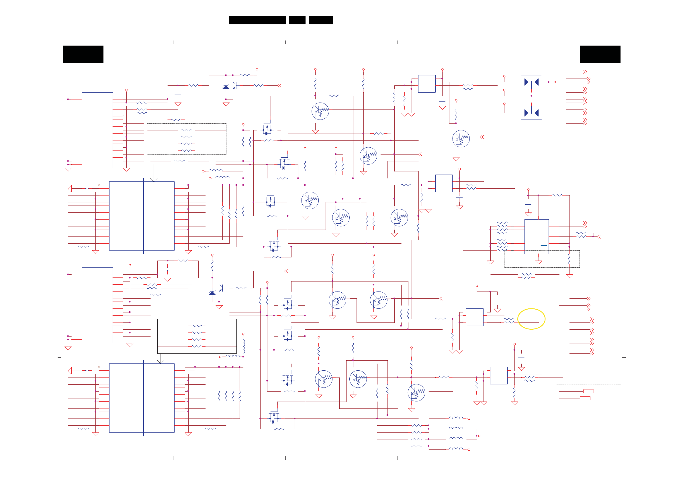
SCALER BOARD: HDMI INPUT
R43
10K/NC
R73
APHD
Q21
BPHD
3
1
1
2
MMBT3904
L135
R75 10K/NC
2
1 2
BPDDC-SCL
BPDDC-SDA
L132
C
47K/NC
R118
R117 10K/N
4
10K
1 2
Q10
R76 47K/NC
R89
4.7K
UDZ5V6B
APDDC-SCL
APDDC-SDA
L134
KHB0805R121SA
+5VS
1 2
R758 0R
BPHD
D7
P1_CBL5V
1 2
R760 0R
APHD
D5
APHD
APDDC-SDA
APDDC-SCL
KHB0805R121SA/NC
P1_CBL5V
1
R83
10K
2
3
1
1
MMBT3904
2
BPCEC-HDMI
BPDDC-SCL
BPDDC-SDA
KHB0805R121SA
R116 10K/NC
R649
0R/NC
2_
HDMI0
21
SHELL2
23
D D
22
20
CN4
HDMI_con
C48
0.1uF
APR0X2+
APR0X2APR0X1+
C C
APR0X1APR0X0+
APR0X0APR0XC+
APR0XCAPRX-CEC
APRX-DDC-SCL
APRX-DDC-SDA APDDC-SDA
APRX-HOTPLUG
1 2
R759 0R
Put the resistance between U7 and CN4
SHELL4
SHELL3
SHELL1
DDC DATA
DDC CLK
CE Remote
CK Shield
D0 Shield
D1 Shield
D2 Shield
12
HP DET
+5V
GND
CK-
CK+
D0-
D0+
D1-
D1+
D2-
D2+
38
37
36
35
34
33
32
31
30
29
28
27
26
25
24
23
22
21
20
HDMI1
21
SHELL2
23
B B
22
20
CN5
HDMI_con
C53
0.1uF
BPR0X2+
BPR0X2BPR0X1+
BPR0X1BPR0X0+
BPR0X0BPR0XC+
A A
BPR0XCBPRX-CEC
BPRX-DDC-SCL
BPRX-DDC-SDA
BPRX-HOTPLUG
1 2
R761 0R
Put the resistance between U9 and CN5
HP DET
SHELL4
SHELL3
SHELL1
+5V
GND
DDC DATA
DDC CLK
CE Remote
CK-
CK Shield
CK+
D0-
D0 Shield
D0+
D1-
D1 Shield
D1+
D2-
D2 Shield
D2+
CONNECTOR IC
38
12
37
36
35
34
33
32
31
30
29
28
27
26
25
24
23
22
21
20
P0_CBL5V
19
R52 1K
18
17
R53 0R
16
R54 0R
15
14
NC
13
12
11
10
9
8
7
6
5
APR0X1+
4
3
2
1
NC
ESD_BYP
GND
1TMDS_D2+
1TMDS_GND
1TMDS_D21TMDS_D1+
TMDS_GND
1TMDS_D11TMDS_D0+
TMDS_GND
1TMDS_D01TMDS_CK+
TMDS_GND
1TMDS_CK1CE_REMOTE_OUT
1DDC_CLK_OUT
1DDC_DAT_OUT
1HOTPLUG_DET_OUT
P1_CBL5V
19
R861K
18
17
16
15
14
NC
BCE Remote
13
12
11
10
9
8
7
6
5
4
3
2
1
NC
ESD_BYP
GND
1TMDS_D2+
1TMDS_GND
1TMDS_D21TMDS_D1+
TMDS_GND
1TMDS_D11TMDS_D0+
TMDS_GND
1TMDS_D01TMDS_CK+
TMDS_GND
1TMDS_CK1CE_REMOTE_OUT
1DDC_CLK_OUT
1DDC_DAT_OUT
1HOTPLUG_DET_OUT
5
APRX-HOTPLUG
12
1 2
1 2
ACE Remote
APR0XC-
APR0XC+
APR0X0-
APR0X0+
APR0X1-
APR0X2-
APR0X2+
APRX-DDC-SCL
APRX-CEC APCEC-HDMI
APRX-DDC-SCL
APRX-DDC-SDA
APRX-HOTPLUG
ACE Remote BCE Remote
ICCONNECTOR
5V_SUPPLY
LV_ SUPPLY
TMDS_D2+
TMDS_GND
TMDS_D2-
TMDS_D1+
TMDS_GND
TMDS_D1-
TMDS_D0+
TMDS_GND
TMDS_D0-
TMDS_CK+
TMDS_GND
TMDS_CK-
CE_REMOTE_IN
DDC_CLK_IN
DDC_DAT_IN
HOTPLUG_DET_IN
U7
CM2021
BPRX-HOTPLUG
12
R870R
R88 0R
BPR0XC-
BPR0XC+
BPR0X0-
BPR0X0+
BPR0X1-
BPR0X1+
BPR0X2-
BPR0X2+
12
12
R90 0R/NC
1 2
BPRX-CEC
BPRX-DDC-SCL
BPRX-DDC-SDA
BPRX-HOTPLUG BPHD
5V_SUPPLY
LV_ SUPPLY
TMDS_D2+
TMDS_GND
TMDS_D2-
TMDS_D1+
TMDS_GND
TMDS_D1-
TMDS_D0+
TMDS_GND
TMDS_D0-
TMDS_CK+
TMDS_GND
TMDS_CK-
CE_REMOTE_IN
DDC_CLK_IN
DDC_DAT_IN
HOTPLUG_DET_IN
U9
CM2021
R56 0R/NC
1 2
GND
BPRX-DDC-SDA
BPRX-DDC-SCL
GND
1 2
6
0.1uF
C4
APRX-CEC
R58 0R/NC
1 2
R62 0R/NC
1 2
R63 0R/NC
1 2
R64 0R/NC
1 2
R704 0R
1 2
2007/03/05 add
BPRX-CEC
P0_CBL5V
1
2
3
APR0X2+
4
5
APR0X2-
6
APR0X1+
7
8
APR0X1-
9
APR0X0+
10
11
APR0X0-
12
APR0XC+
13
14
APR0XC-
15
APCEC-HDMI
16
APDDC-SCL
17
18
19
R82 0R/NC
1 2
0.1uF
C50
UDZ5V6B
2007/03/05 modify PB to BP
R99 0R/NC
1 2
R100 0R/NC
1 2
R102 0R/NC
1 2
R103 0R/NC
1 2
1
2
3
BPR0X2+
4
5
BPR0X2-
6
BPR0X1+
7
8
BPR0X1-
9
BPR0X0+
10
11
BPR0X0-
12
BPR0XC+
13
14
BPR0XC-
15
BPCEC-HDMI
16
BPDDC-SCL
17
BPDDC-SDA
18
19
P0_CBL5V
1 2
2
4.7K
DDC_VCC
3
1
1
10K
2
2
R60 10K
R59
R74 47K
2N7002/NC
1
10K
R9
+5VS
L133
KHB0805R121SA/NC
R119 47K
R46
2
0R
R61
Q15
2N7002/NC
3
R67
2
3
R77 0R/NC
Q20
3
R81 0R/NC
DDC_VCC
1
1
2
2
R92 10K
R95 0R
Q25
2N7002/NC
3
R120 0R/NC
APHD_CRL
Q12
2N7002/NC
1
12
2
1
0R
12
Q16
2N7002/NC
1
12
2
1
12
BPHD_CRL
2
3
12
2
3
R105 0R
2
3
R113 0R/NC
2
Q30
2N7002/NC
1
12
R44
DDC_VCC
1
2
3
2
Q24
2N7002/NC
1
1
12
Q26
2N7002/NC
1
12
DDC_VCC
1
1K/NC
2
R50
3
2
Q11
DTC144E/NC
R65
1K/NC
1
Q17
DTC144E/NC
2_
DDC_VCC
1
R106
1K/NC
2
3
2
DTC144E/NC
10K/NC
1 2
1
DDC_VCC
1
R66
1K/NC
2
3
2
DDC_VCC
1
2_
R84
2
3
2
DTC144E/NC
1
Q27
2
1
DTC144E/NC
1K/NC
Q22
R104
1K/NC
3
DDC_VCC DDC_VCC
2
2
R51
0R
1
1
ADVI_SDA
ADVI_SCL
APCCE_SW
R68
0R/NC
1 2
3
Q19
2
DTC144E/NC
1
R93 10K/NC
2
BCE_SDA
BCE_SCL
24LC02B_SOP_8P
1
A0
2
A1
3
A2
VSS4SDA
1
1
2
BPCCE_SW
NC
1
10K/
4
R9
2
BDVI_SDA
BDVI_SCL
DDC_VCC
2_
1
R107
10K/NC
2
3
2
DTC144E/NC
R754 1.8K
R755 1 .8K
R756 1 .8K
R757 1 .8K
R72
10K/NC
1
Q18
1
DDC_VCC
1
R45
1K/NC
2
3
2
2_
1
2
3
Q28
2
DTC144E/NC
APCCE_SWAPRX-DDC-SDA
10K/NC
R57
1 2
1
Q14
DTC144E/NC
NC
1
1
10K/
R78
R79 10K/NC
2
2
DDC_VCC
1
R85
1K/NC
2
3
2
DTC144E/NC
1
1
R114 10K/NC
2
APRX-DDC-SCL
APRX-DDC-SDA
BPRX-DDC-SCL
BPRX-DDC-SDA
R47
0R/NC
ACE_SDA
ACE_SCL
2_
1
Q23
1
NC
10K/
2
12
R1
U5
8
VCC
EDID_WP
7
WP
6
SCL
5
7
1uF
0.
C4
APCCE_SW
U6
24LC02B_SOP_8P/NC
1
A0
VCC
2
A1
WP
3
A2
2
1
R80
0R/NC
Q29
R71 NC
SCL
VSS4SDA
BPCCE_SW
0R/NC
R96
1 2
R101
0R
R108 0R/NC
1 2
BPCCE_SW
1
KHB0805R121SA
KHB0805R121SA/NC
KHB0805R121SA/NC
KHB0805R121SA
R48 47
R49 47
EDIT_WP
DDC_VCC
2
1
3
2
DDC_VCC
8
7
6
5
2
1
L130
L131
L137
L138
2
1 2
1 2
2_
R55
10K
1
Q13
DTC144E
EDID_WP
R69 47/NC
1 2
R70 47/NC
1 2
C49
0.1uF
APDDC-SCL
BPDDC-SCL
APDDC-SDA
BPDDC-SDA
DDC_VCC
U8
24LC02B_SOP_8P
1
A0
VCC
2
A1
3
A2
SCL
VSS4SDA
R111
NC
P0_CBL5V
P1_CBL5V
P0_CBL5V
2_
ADVI_SCL
ADVI_SDA
DDC_WP
ACE_SCL
ACE_SDA
R633 0R
1 2
R6340R
1 2
R6350R
1 2
R6360R
1 2
R6390R
1 2
R640 0R
1 2
R641 0R
1 2
R642 0R
1 2
APDDC-SCL
APDDC-SDA CE_SDA
8
EDID_WP
7
WP
2
1
R97 47
6
R98 47
5
U10
24LC02B_SOP_8P/NC
1
A0
VCC
2
A1
3
A2
SCL
VSS4SDA
DDC_VCC
1 2
DDC_VCC
2_
D6
P1_CBL5V
BAV70
DDC_VCC
C435
0.1uF
R644 0R/NC
1 2
R645 0R/NC
1 2
0.1uF
C51
1 2
1 2
DDC_VCC
8
7
WP
6
5
2
R115
NC
1
5
4
3
10
11
12
13
BDVI_SCL
BDVI_SDA
2_
EDID_WP
R109 47 /NC
1 2
R110 47/NC
1 2
3
3
1
2
U54
16
PI5C3253
C
1B161A
1B2
VC
1B3
1B4
2B1
1OE
2B2
2OE
2B3
2B4
GND
8
1uF
0.
C52
BCE_SCL
BCE_SDA
D4
BAV70
+5VS
12
R632NC
1 2
7
9
2A
14
S0
2
S1
1
15
CE_SCL
APHD
APDDC-SDA
APDDC-SCL
APR0XCAPR0XC+
APR0X0APR0X0+
APR0X1APR0X1+
APR0X2APR0X2+
R6370R
1 2
R638 0R
1 2
2
R643
0R
1
BPHD
BPDDC-SDA
BPDDC-SCL
BPR0XCBPR0XC+
BPR0X0BPR0X0+
BPR0X1BPR0X1+
BPR0X2BPR0X2+
+3V3-TMDS341
+5VS
1
APHD
APDDC-SDA
APDDC-SCL
APR0XCAPR0XC+
APR0X0APR0X0+
APR0X1APR0X1+
APR0X2APR0X2+
CE_SCL
CE_SDA
HDMI_SEL
BPHD
BPDDC-SDA
BPDDC-SCL
BPR0XCBPR0XC+
BPR0X0BPR0X0+
BPR0X1BPR0X1+
BPR0X2BPR0X2+
+3V3-TMDS3414
+5VS 2,3 ,4,6,10,11
I_17540_019.eps
310108
Page 23
Circuit Diagrams and PWB Layouts
Scaler Board: HDMI Switch
5
23QCS1.0S LA 7.
4
3
2
1
S-A03 S-A03
BPR0XCBPR0XC+
BPR0X0BPR0X0+
BPR0X1BPR0X1+
BPR0X2BPR0X2+
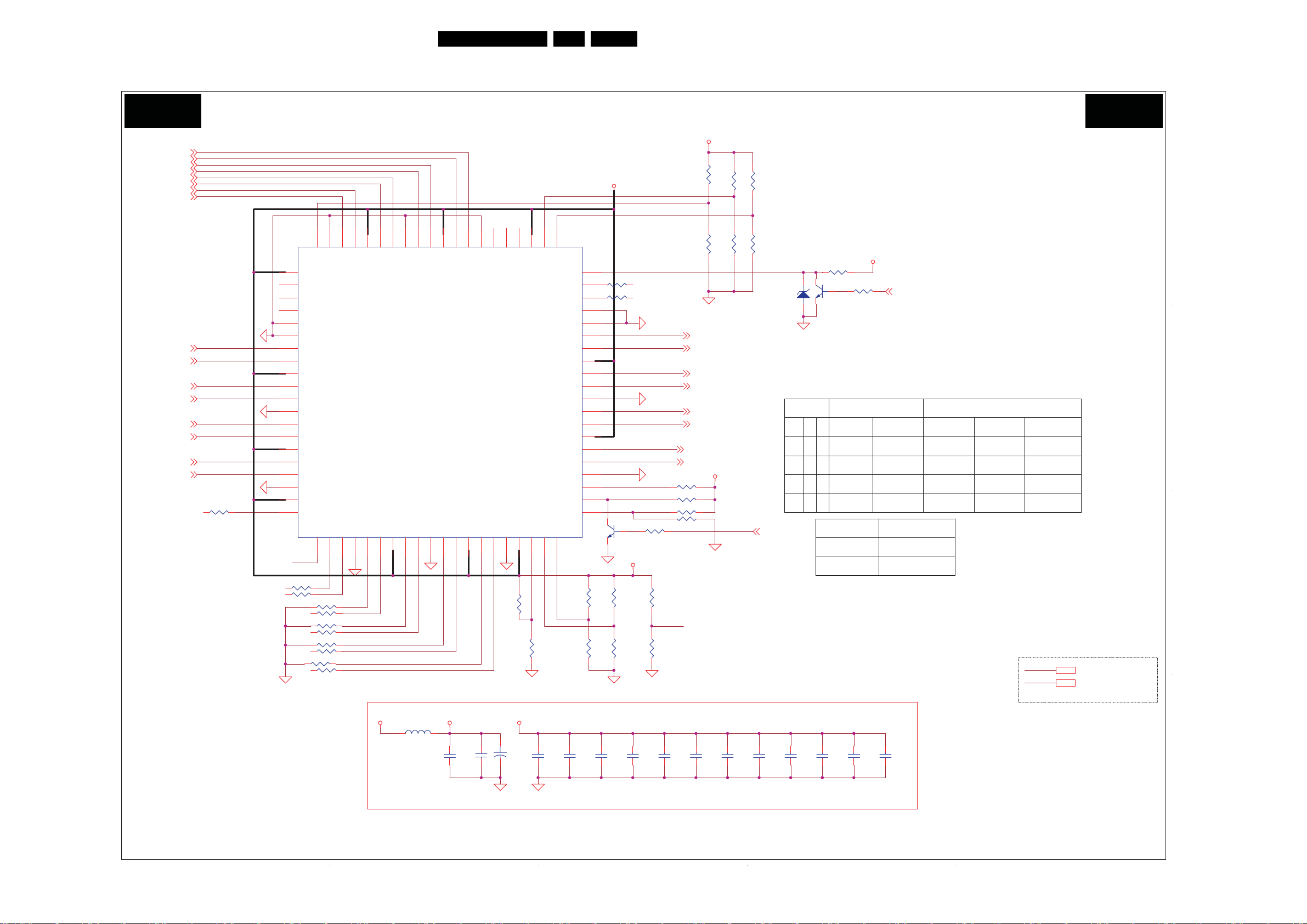
SCALER BOARD: HDMI SWITCH
BPR0XC-
BPR0XC+
BPR0X0-
BPR0X0+
BPR0X1-
BPR0X1+
BPR0X2-
BPR0X2+
+3V3-TMDS341
TMDS_/OE
EQ_S0
EQ_S1
+3V3-TMDS341
8
R12
27K/NC
0
R13
27K/NC
1
R13
27K/NC
D D
59
60
58
NC4
VCC
HPD2
SDA2
SCL2
GND
GND
B21
A21
VCC
B22
A22
GND
B23
A23
VCC
B24
A24
GND
VCC
HPD1
GND
SDA12SCL1
NC1
3
1
61
62
63
64
65
66
APR0XC-
APR0XC+
APR0X0-
C C
APR0X0+
APR0X1-
APR0X1+
APR0X2-
APR0X2+
APR0XC-
APR0XC+
APR0X0-
APR0X0+
APR0X1-
APR0X1+
APR0X2-
APR0X2+
R126NC
12
67
68
69
70
71
72
73
74
75
76
77
78
79
80
OC_S0
55
56
3
C
B3457A34
VC
0228_EC
GND4B115A11
6
B3354A3
VCC
7
53
52
GND
U11
TMDS341
2
B1
A129GND
8
B3251A32
10
49
50
VCC
B1311A1312VCC
43
VCC
VSADJ18PRE
41
42
/OE
HPD_SINK
SDA_SINK
SCL_SINK
20
19
NC3
GND
GND
VCC
GND
VCC
GND
NC2
40
39
38
37
36
35
Z1
34
Y1
33
32
Z2
31
Y2
30
29
Z3
28
Y3
27
26
Z4
25
Y4
24
23
S3
22
S2
21
S1
Q37
MMBT3904
R702 NC
1 2
R703 NC
1 2
3
2
1
+3V3-TMDS341
HPD
RXC-
RXC+
RX0-
RX0+
RX1-
RX1+
RX2-
RX2+
R148 4.7K
R149 4.7K
R151 4.7K/NC
1 2
R153
4.7K
RXC-
RXC+
RX0-
RX0+
RX1-
RX1+
RX2-
RX2+
1 2
1 2
1 2
R155 0R
R135
+3V3-TMDS341
12
0R/NC
0R
R136
UDZ5V6B/NC
R137
0R/NC
D58
HDMI_SEL
1
2
Control
Pins
S1
H
XX
LHX
L
L
L
R662 10K
1 2
3
R663 4.7K/NC
2
1 2
Q70
1
MMBT3904/NC
I/O SELECTED
Y/ Z
A1/B1
A2/B2
A3/B3
H
None(Z)
HDMI_SEL
L
H
DDC_VCC
SCL_SINK
SDA_SINK
SCL1
SDA1
SCL2
SDA2
SCL3
SDA3
None(Z)L
HDMI PORT
APHD_CRL
HDMI0
HDMI1
HOT PLUG DETECT STATU S
HP D1
HPD_SINK
HP D2 HP D3S2S3
L
L
LH
L
L
L
L
LHPD_SINK
HPD_SINK
L
45
47
B3148A31
GND
4
B1
13
14
44
46
SCL3
SDA3
HPD3
4
A1
GND
VCC
17
15
16
R121NC
B B
12
R122NC
12
R124 1K
1 2
R123NC
12
R127 1K
1 2
R125NC
12
R1321K
1 2
R129NC
12
R1341K
1 2
R133NC
12
2007/04/12 For power saving wake up
+3.3AV DD
KHB0805R121SA
L17
+3V3-TMDS341
C456
1nF
C469
0.1uF
R160
27K/NC
%
R162
4.64K_ 1
+3V3-TMDS341
C455
+
10uF/50V
7
R15
3
R16
27K/NC
0R/NC
R158
OC_S1
OC_S3
OC_S2
27K/NC
9
C
R15
27K/N
OC_S0
0R
R165
R164
0R/NC
pin7, 13 , 17, 27, 33,43 , 50, 56, 61, 69, 75, 79
C457
0.1uF
C458
0.1uF
C459
0.1uF
C460
0.1uF
C461
0.1uF
C462
0.1uF
C463
0.1uF
C464
0.1uF
C465
0.1uF
C466
0.1uF
C467
0.1uF
C468
0.1uF
+3V3-TMDS341
+3.3V_SW
+3V3-TMDS341 3
+3.3V_SW 2,9,10,11,15,16
A A
CloseToTMDS341
I_17540_020.eps
310108
5
4
3
2
1
Page 24
Circuit Diagrams and PWB Layouts
Scaler Board: Analog Input
5
24QCS1.0S LA 7.
4
3
2
1
S-A04 S-A04
D D
17
16
SYN_7519S_15G2_08
C C
MINA_YKC31_0183V_5P/NC
P5
P4
P3
P2
B B
A A
P1
MINI_YKC31_0185V_3P
CN8
P3
P3
P2
P2
P1
P1
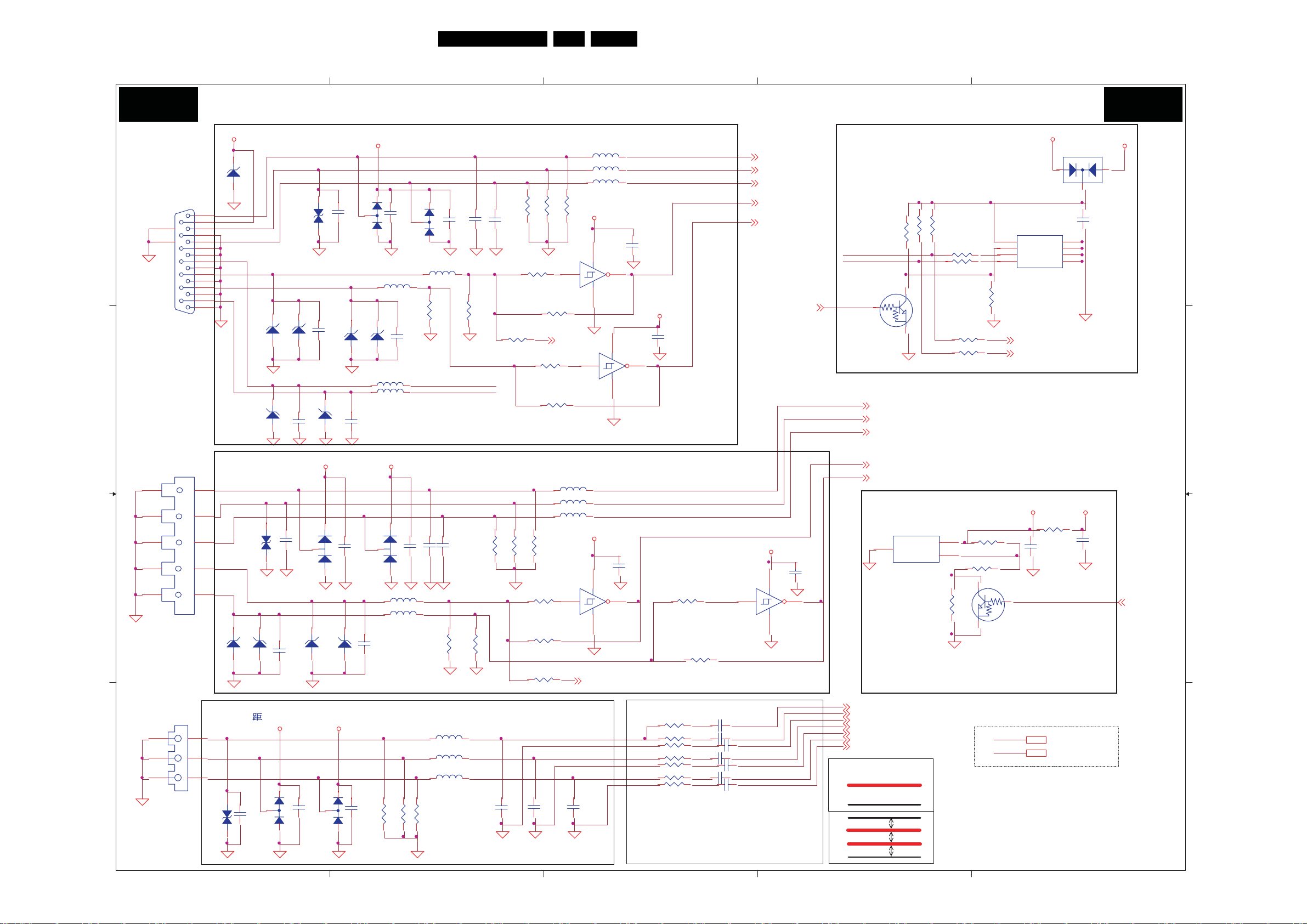
SCALER BOARD: ANALOG INPUT
CN6
CN7
VGA_5V
1
2
D9 UDZ5V6B
1
9
2
10
3
11
4
12
5
13
6
14
7
15
8
G5
G4
G3
G2
G1
BNC_V
LP8/NC
1
2
D2
A_M
2
402ESD
Y_0
POL
G3
G3
G2
G1
G1
1
2
D26 EZJZ0V8 00AA/NC
5
1
LP8/NC
D13
2
POLY_0402ESDA_M
1
UDZ5V6B
2
D18
2007/04/12 C67/C68 change from 0.1uFto47pF
1
2
D19
EZJZ0V800AA/NC
BNC_H
1
4UDZ5V6B/NC
2
D2
C78 47pF
+5VS
2
NC
3
1
6
C43
D27 BAV99
1
2
EZJZ0V800AA/NC
D12
1
C6447pF
2
D15 UDZ5V6B
1
2
D17 UDZ5V6B
C67 47pF
+5VS +5VS
2
3
C71 NC
1
BAV99/NC
D20
NC
1
LP8/
M
D23
2
POLY_0402ESDA_
+5VS
C
3
C81N
8 BAV99
D2
2007/04/12 C81/C82/C436NC
D14
Z5V6B/NC
5UD
D2
2
1
+5VS
2
V99
BA
3
C59 NC
1
D8
L19 0R
2
LP8/NC
1
1
DA_M
S
6 UDZ5V6B
2
2
D1
POLY_0402E
L20 0R
1
L21 0R
1
C68 47pF
3
D21
C72 NC
BAV99/NC
L22 0R
2
L23 0R
2
1
C79 47pF
2
75_1/2W
C82NC
R210
C
C57 N
547pF
C6
2
2
2
1
75_1/2W
R211
2
3
1
D10 BAV99
L18 0R
1
2.2K
R189
C73 NC
C75 NC
1
1
R202
2.2K
L116 0R
2
L117 0R
2
L118 0R
2
W
2 75_1/2
R21
4
:16
C58 NC
12
R188 2.2K
DDC_VGA_SDA
DDC_VGA_SCL
: 16mil
C76 NC
R203
2.2K
1
1
1
75_1/2W
9
C60 NC
R745 100
R17
C61 NC
R186 100
R682 0R/NC
EC_0608
R192 100
EC_0606_CSYNC
R683 0R/NC
/NC
75_1/2W/NC
R198 75_1/2W/NC
R197 75_1/2W
C83
NC
R199
R194 100
R684 0R/NC
R748 100
NeartoCN8
75_1/2W
75_1/2W
R180
R181
2 4
1
DSUB_H_CSYNC
L113 0R
2
L114 0R
2
L115 0R
2
U18
NC7S14/NC
2 4
1
C84
NC
L110 0R
2
L111 0 R
L112 0R
2
SMTVCC
SMTVCC
BNC_H_CSYNC
C85
NC
5
3
2
1
1
1
1
5
3
U16
NC7S14
5
3
1
12
1
U17
NC7S14
DSUB _RIN
DSUB_GIN
DSUB_BIN
DSUB _HIN
DSUB_VIN
C63
0.1uF
SMTVCC
C66
0.1uF
4
Near to CN6
SMTVCC
C69
0.1uF
R200 100
R685 0R/NC
2
1
U19
NC7S14/NC
5
4
3
NeartoCN7
1
R284 470
R283 33
R28275
R281 33
R28075
R286 33
R28575
2
1
2
1
2
1
2
1
2
1
2
1
C169 47nF/25V
1
C168 47nF/25V
C167 47nF/25V
1
C166 47nF/25V
C172 47nF/25V
1
C171 47nF/25V
BNC_SOG
BNC_Y+
2
BNC_Y-
2
1
2
1
2
1
BNC_PB+
BNC_PB-
2
BNC_PR+
2
BNC_PR-
C170 1nF
2
1
2
Near to U29A(MST5251A)
3
DDC_WP
C70
0.1uF
DDC_VGA_SCL
DDC_VGA_SDA
1
Q43
DTC144E
BNC_RIN
BNC_GIN
BNC_BIN
BNC_HIN
BNC_VIN
ANA_AP431AWLA_SOT23_3P
BNC_SOG
BNC_Y+
BNC_YBNC_PB+
BNC_PBBNC_PR+
BNC_PR-
16mil
GND: 8mil atleast
R+
R-
2
10K
R175
3
2
R18210K
R183 10K
R184100
R185 100
R190 0R
R191 0R
R187
NC
8
VCC
7
WP
6
SCL
5
SDA
24LC02B_SOP_8P
VGA_SCL
VGA_SDA
+5VS
U15
GND
D11
BAV70
2
C62
0.1uF
1
A0
2
A1
3
A2
4
VGA_5 V
1
3
Near to CN6
C77
0.1uF
+5VSB
SMT
SMTVCC
U20
2
Cathode
3
Anode
REF
R204 2.2K
1
R205 6.8K
R207
22K
3
DTC144E
2
R201 470
C80
0.1uF
1
Q44
Near to U16/U17 and
don't be too far
from U18/U19
+5VSB
+5VS
7mil
8mil
7mil
+5VSB 2,6,13
+5VS 2,3 ,4,6,10,11
1
I_17540_021.eps
310108
Page 25
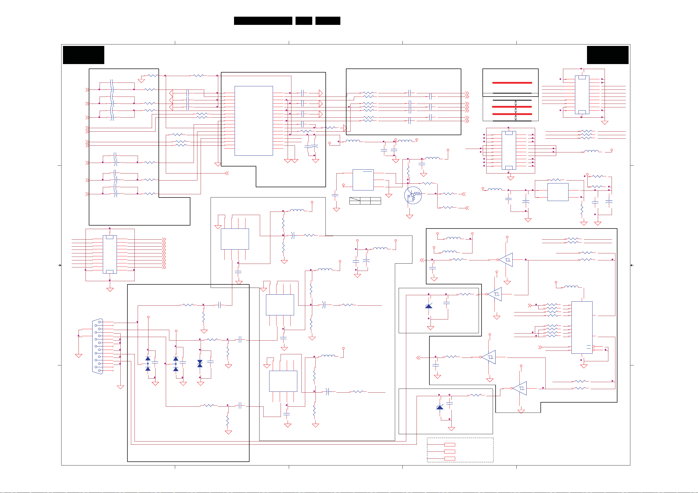
Circuit Diagrams and PWB Layouts
25QCS1.0S LA 7.
Scaler Board: Analog Switch & Output
5
S-A05 S-A05
DSUB_BIN
DSUB_GIN
D D
DSUB_RIN
DSUB_HIN
DSUB_VIN
BNC_HIN
BNC_VIN
BNC_BIN
BNC_GIN
BNC_RIN
SCALER BOARD: ANALOG SWITCH & OUTPUT
C860R
C8747uF/25V/NC
C90 0R
C92 47uF/25V/NC
C95 0R
C97 47u F/25V/NC
DSU B_HIN
DSUB_VIN
BNC_HIN
BNC_VIN
C106 0.01uF
C108 47uF/25V/NC
C109 0.01uF
C110 47u F/25V/NC
C111 0.01uF
C112 47u F/25V/NC
R213 NC
+
+
+
+
+
+
R215 0R
R219 0R
R223 0R
R234
33
R237
33
R238
33
R228 100
R214 10K
DSUB_BLU_IN
C88 0.01uF
C91 0.01uF
C94 0.01uF
R222 NC
R224 NC
R229 NC
R231NC
RGB_SEL
DSUB_GRN_IN
DSUB_RED_IN
Near to U21
:
C C
24
RPEAK1
RPEAK2
RPEAK3
GPEAK1
GPEAK2
GPEAK3
BPEAK1
BPEAK2
BPEAK3
B B
17
16
SYN_7519S_15G2_08
A A
1 2
3
5
7
9
11
13
15
17
19
CN9
21
22
23
1
9
2
10
3
11
4
12
5
13
6
14
7
15
8
2007/06/04 Modify by Kodi
J4 1000-E20E-04R /NC
RPEAK1
4
6
8
10
12
14
16
8
1
20
RPEAK2
RPEAK3
GPEAK1
GPEAK2
GPEAK3
BPEAK1
BPEAK2
BPEAK3
2007/06/04 Modify byKodi
Near to CN9
RED_OUT GREENOUT
+5V_SW
3
VS_OUT
HS_OUT
D29 BAV99
RPEAK1
RPEAK2
RPEAK3
GPEAK1
GPEAK2
GPEAK3
BPEAK1
BPEAK2
BPEAK3
R240
75_1/2W
+5V_SW
GREEN_OUT
2
1
2
AV9 9
NC
3
C114
1
D33 B
BLUE_OUT
C119 NC
R244
220K
1
D3
EZJZ0V800AA/NC
C116
100uF/25V
1
2
R258
75_1/2W
2
R251
75_1/2W
4
U21
MTM_MM1470AJBE_SSOP_34P/NC
1
VooI-R
2
Rin1
3
VooI-G
4
Gin1
5
VooI-B
6
Bin1
7
Hin1
8
Vin1
9
GND
10
Rin2
11
Power_Save
12
Gin2
13
SW
14
Bin2
15
Hin2
16
Vin2
17
NC1
RGB_SEL
4
3
2
1
IN
NC1
-VSS
NC4
5
0.1uF
1
NC2
+VCC
OUT
NC3
7
6
8
C113
2007/03/07 change the package
TSH340IDT
0226-4 NET error
C122
100uF/25V
2
1
R253
220K
C124 NC
C128
100uF/25V
2
1
R260
220K
Voo2-R
Rout
GND-R
Voo2-G
Gout
GND-G
Voo2-B
Bout
GND-B
Sync_on_G
Sync_in
Sync_out
Hout
Vout
GND
NC2
Middle
of U29A
& CN6
U24
TSH340IDT
U27
U28
TSH340IDT
Vo o
4
5
-VSS
NC4
C120
0.1uF
4
5
34
33
32
31
30
29
28
27
26
25
24
23
22
21
20
19
18
3
6
-VSS
NC4
0.1uF
HOUT
VOUT
L26
KHB0805R121SA
R239
33K
C115 100uF/25V
R243
10K
2
1
IN
NC1
NC2
+VCC
OUT
NC3
7
8
2
3
IN
NC1
+VCC
OUT
7
6
C125
C89 0.01uF
C93 0.01uF
C96 0.01uF
C101 0.01uF
uF
+
C105 0.01
AMP5V
L27
KHB0805R121SA
R249
33K
C121 100uF/25V
R252
L28
KHB0805R121SA
R226
REDOUT
2
10K
R257
33K
C127 100uF/25V
R259
10K
R686NC
1
+
R217 47
1
NC2
NC3
8
3
R271 33
1
SW_BLU_A
SW_GNDB
SW_GNDG
SW_GNDR
1M
ANA5V
uF/25V/NC
C104 47
C432
AMP5V
2007/03/07 change the package
1
+
R221 47
AMP5V
2007/03/07 change the package
+
R272 75
1
R273 470
1
R275 33
1 2
R276 75
1
R277 33
1
R278 75
1
Near to U29A(MST5251A)
L119 0R
U56
4
BP
ANB5V
5
VOUT
APL5151-50BC/NC
0.33uF
SHDN
AMP5V
C438
0.1uF
2
1
R225 47
2
2
2
2
2
2
3
SHDN
2
GND
1
VIN
ON OFF
HI LOW
L120
KHB0805R121SA
+
7uF/25V
C4374
2
BLUEOUT
BLUEOUT
GND_OUTB
GND_OUTG
REDOUTSW_RED_A
C107
C159 47nF/25V
1 2
C160 47nF/25V
2
1
SOGOUT SOG
GREENOUT GREEN+SW_GRN_A
C161 1nF
1
C163 47nF/25V
1 2
C165 47nF/25V
1
2
ANB5V
0.01uF
ANA5V
+5VSB
L136KHB0805R121SA
C103
1uF
R230
10K/NC
3
2
DTC144E/NC
AHS
HS_OUT
UDZ5V6B
2
C162 47nF/25V
2
1
C164 47nF/25V
1 2
2007/06/04 Modify byKodi
+5VSB
L25
KHB0805R121SA/NC
C477
1uF
R232
0R
+3.3AV DD
ANB5V
KHB0805R121SA/NC
C117
NC
1
2
R233
100
R236
NC
KHB0805R121SA
L123
R241 100
1
Q45
D30
Near to CN9
VS_OUT
D32
UDZ5V6B
R254 100
C123
NC
1
2
AV S
2
BLUE+
BLUE-
GREEN-
RED+
RED-GND_OUTR
BLUE+
BLUE-
SOG
GREEN+
GREEN-
RED+
RED-
EQ-12V
ANB5V
STBY
2007/06/04 L24/Add
ANAP_SD
KHB0805R121SA/NC
Near to U21
SYNC_B+
L122
U25B
74LCX14MX
R245 100
C118
47pF
74LCX14MX
R256 100
C126
47pF
Near to CN9
4
SYNC_B+
U25C
6
GND: 8mil atleast
R+
R-
24
21
1
3 4
5
7
9
11
13
15
17
19
23
22
L24
C98
0.1uF
SYNC_B+
14
2
SYNC_B+
7
14
3
7
14
5
7
8
7mil
8mil
7mil
2
6
8
10
12
14
16
18
20
C99
+
10uF/50V
U25A
74LCX14MX
1
CSYNC_H
BNC_HIN
DSUB_HIN
BNC_VIN
CSYNC_S EL
SYNC_B+
74LCX14MX
14
7
1
21
24
J6
1000-E20E-04R /NC
R727 100
R728 100
R247 100
R246 100
R729 100
R730 100
R250 100
R248 100
U25D
9
SW_BLU_A
SW_GNDB
SW_GRN_A
SW_GNDG
SW_RED_A
SW_GNDR
DSUB_BLU_IN
DSUB_GRN_IN
DSUB_RED_IN
2
4
DSUB_VIN
DSU B_HIN
VIN
VOUT
OUT
ADJ/GND
AP1117ELA/TO223
R721 0R
R722 0R
HOUT
ANB5V
KHB0805R121SA/NC
RGB_SEL
VOUT
1 2
3
5 6
7 8
9 10
11
13 14
15 16
17
19 20
J3
1000-E20E-04R /NC
EQ-12V
R218
110/1%
U22
3
1
R227
330/1%
1
1
R687NC
R242 100
EC_0606_CSYNC
U26 is changed
L129
13
I3B
12
I2B
11
I1B
10
I0B
3
I3A
4
I2A
5
I1A
6
I0A
2
S1
14
S0
R688 NC
R255 100
22
23
R718 0R
1 2
R719 0R
1
R720 0R
1
L126
KHB0805R121SA
+12V_SW
2
2
U26
16
74HCT153DT/NC
C
VC
YB
YA
Eb
Ea
GND
8
4
12
18
2
2
R216
75_1/2W
R220
75_1/2W
9
7
15
1
C102
0.1uF
VOUT_A
HOUT_A
Middle of U21 & CN9
BLUEOUT
GND_OUTB
SOGOUT
GREENOUT
GND_OUTG
REDOUT
GND_OUTR
SW_BLU_A
SW_GRN_A
SW_RED_A
+12V_SW
+
470uF/16V
HOUT_A
VOUT_ADSUB_VIN
C100
+3.3AV DD
+5VSB
l
5
4
3
+12V_SW
+3.3AVDD 2,7
+5VSB2,5,13
+12V_SW 2,10,11,12,14
2
I_17540_022.eps
1
310108
Page 26
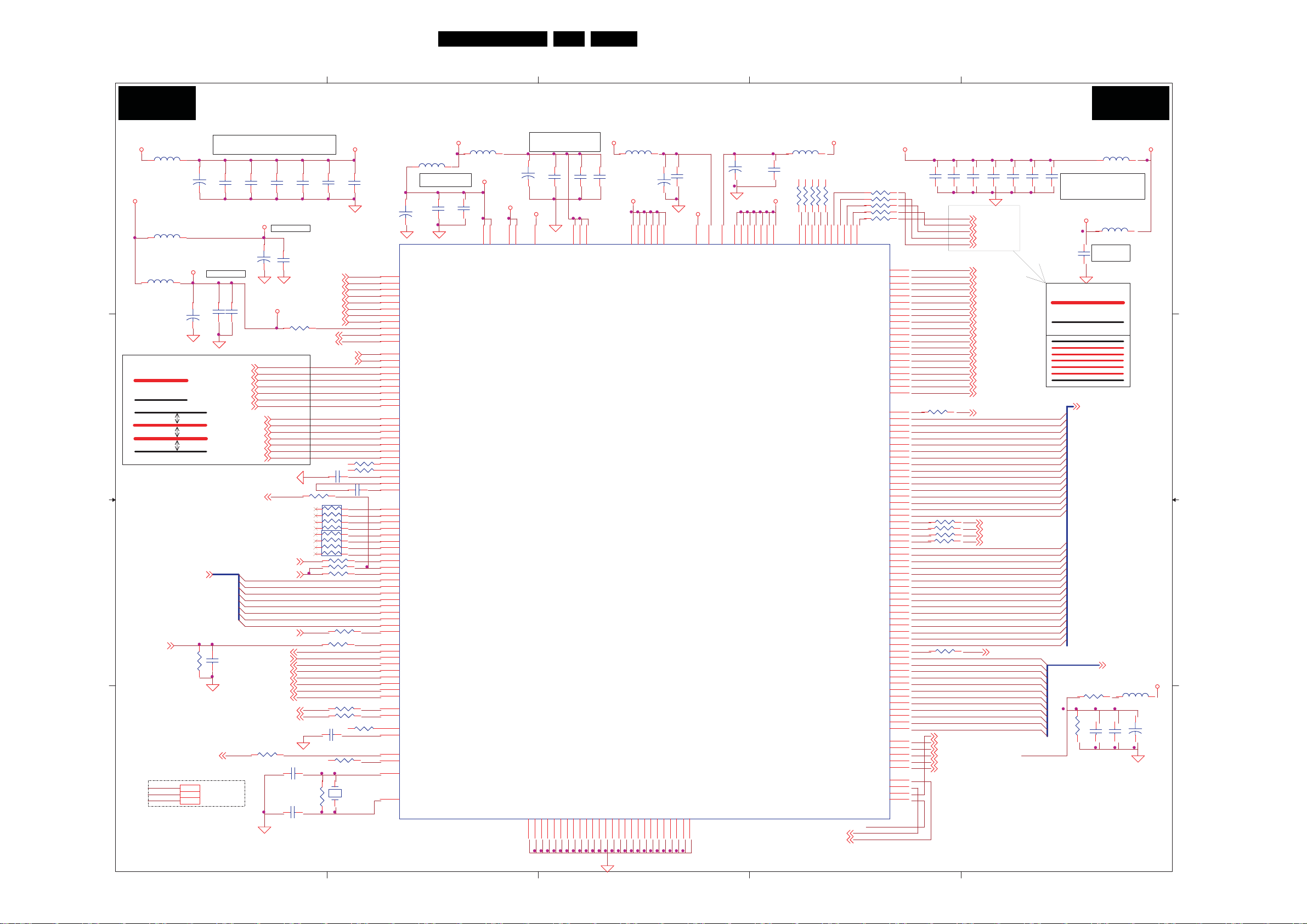
Circuit Diagrams and PWB Layouts
26QCS1.0S LA 7.
Scaler Board: Scaler
5
S-A06 S-A06
2.5V_MEM VDDM
KHB0805R121SA
22uF/50V
+3.3AV DD VDDM
D D
L35KHB0805R121SA
L36
KHB0805R121SA
16mil
GND: 8mil atleast
C C
R+
R-
B B
HWRESET
A A
1.8V_MST
2.5V_MEM
+3.3AV DD
SCALER BOARD: SCALER
L33
C132
AVDD2
7mil
8mil
7mil
R298
10K
RL_HRLL
uF/25V
C156 47
pin86,102,113,125,139,154
1
1
C146
C145
+
0.1uF
0.1uF
2
2
pi n4,10
.1uF
1
1
1
+
2
2
C157 0.1uF
BLUE+
BLUESOG
GREEN+
GREENRED+
RED-
UD_HULD
2
1
C175
0.1uF
2
1
1.8V_MST2
2.5V_MEM 2
+3.3AVDD 2,6
0
2
C158
BNC_PBBNC_PB+
BNC_YBNC_Y+
BNC_SOG
BNC_PRBNC_PR+
1
1
C147
0.1uF
2
2
AVDD1
pi n204
1
+
2
C155 22uF/50V
AV D D2
BLUE+
BLUESOG
GREEN+
GREENRED+
RED-
SHS
VLLCVD[0:7]
SVS
SCALER_INT
SCALER_ALE
SCALER_RD
SCALER_WR
SCALER_AD0
SCALER_AD1
SCALER_AD2
SCALER_AD3
PWM0
PWM1
R303 0R
1
C180 22pF
C18122pF
1
C149
C148
0.1uF
0.1uF
2
1
40.1uF
2
C15
R270
390
CE_SDA
CE_SCL
BNC_PBBNC_PB+
BNC_Y-
BNC_Y+
BNC_SOG
BNC_PRBNC_PR+
C173 0.1uF
R288
1
0R
1
RS20 NC
2
3
4
1
RS21 NC
2
3
4
R292 0R
R293 NC
R294 0R
VD0
VD1
VD2
VD3
VD4
VD5
VD6
VD7
R296 100
C176 0.1uF
2
R304 0R
R305
1M
1
C150
0.1uF
2
RX2+
RX2RX1+
RX1RX0+
RX0RXC+
RXC-
AHS
AV S
R679 NC
1
R680NC
1
2
1
1
C174 0 .1uF
2
8
7
6
5
8
7
6
5
1
1
1 2
R295 0R
1
1
R300 0R
1
1
R301 0R
R681NC
1
2
1
1
1
X1
14.318MHZ
2
1
2
RX2+
RX2RX1+
RX1RX0+
RX0RXC+
RXC-
2
2
2
2
2
2
2
2
207
208
2
3
5
6
8
9
11
14
15
18
19
20
21
22
23
24
25
26
27
28
29
30
31
32
33
36
2
37
2
38
39
40
41
42
43
44
45
46
47
48
51
52
53
54
55
56
57
58
59
60
61
77
67
68
69
70
71
72
73
74
75
200
201
62
2
158
76
78
202
203
KHB0805R121SA
uF/50V
C151 22
4
L34
pi n17,34
1
C152
+
0.1uF
2
DVI _R+
DVI_RDVI_G+
DVI_G-
DVI_B+
DVI_BDVI_CK+
DVI_CKREXT
DDCD_DA
DDCD_CK
HSYNC1
VSYNC1
BIN1
BIN1M
SOGIN1
GIN1
GIN1M
RIN1
RIN1M
BIN0M
BIN0
GIN0M
GIN0
SOGIN0
RIN0M
RIN0
HSYNC0
VSYNC0
RMID
REFP
REFM
VI_DATA[8]
VI_DATA[9]
VI_DATA[10]
VI_DATA[11]
VI_DATA[12]
VI_DATA[13]
VI_DATA[14]
VI_DATA[15]
GPIO[5]/VHS
GPIO[4]/VCLK2
VI_CK
VI_DATA[0]
VI_DATA[1]
VI_DATA[2]
VI_DATA[3]
VI_DATA[4]
VI_DATA[5]
VI_DATA[6]
VI_DATA[7]
GPIO[2]/VVS
HWRESET
INT
ALE
RDZ
WRZ
DBUS[0]
DBUS[1]
DBUS[2]
DBUS[3]
PWM0
PWM1
VCTRL
BYPASS
GPIO[3]/VDE
GPIO[1]/FIELD
XOUT
XIN
+3.3AV DD +3.3AVD D
1
2
C153
0.1uF
L29
KHB0805R121SA
AVDD0
1
2
17
34
AV DD_ADC
AV DD_ADC
AVDD2
C130
4
10
I
I
_DV
DD
AV DD_DV
AV
pin66,162,182
1
+
22uF/50V
2
AVDD1
204
AV DD_MPLL
2
.1uF
0
C135
1
C133 0.1uF
66
VDDP
162
VDDP
C134
182
VDDP
U29A
5251A
6019B0130701
GND
GND
GND
1
GND
7
GND
13
GND
16
GND
35
GND
50
GND
64
GND
65
80
GND
87
GND
103
108
GND
114
126
KHB0805R121SA
0.1uF
22uF/50V
86
VDDM
GND
GND
GND
GND
140
155
132
3
102
VDDM
GND
157
C136
113
M
VDD
GND
163
159
L30
139
125
VDDM
GND
172
1
2
154
VDDM
GND
183
+
VDDM
GND
GND
184
1
2
194
C137
0.1uF
GND
205
VAPLL
GND
GND
206
12
49
AV DD_APLL
109
AV DD_PLL
AV DD_PLL2
1
+
C129
22uF/50V
2
79
63
C
VDD
VDDC
131
VDDC
156
C
VDD
KHB0805R121SA
1
C131
0.1uF
2
VDDC
185
173
195
VDDC
VDDC
VDDC
L31
R261
NC
2
1
199
S
AIW
2
R262NC
1
198
2
R263NC
1
197
AISD
AISCK
+3.3AV DD
2
2
R264NC
R689NC
1
1
196
193
192
SIMCK
SPDIFO
MCLKMCLK+
UTE
AUM
191
AUWS
2
R265 0R
R266 0R
R267 0R
R268 0R
R269 0R
190
189
188
K
K
D
C
MC
AUS
AUS
AU
MDATA[0]
MDATA[1]
MDATA[2]
MDATA[3]
MDATA[4]
MDATA[5]
MDATA[6]
MDATA[7]
MDATA[8]
MDATA[9]
MDATA[10]
MDATA[11]
MDATA[12]
MDATA[13]
MDATA[14]
MDATA[15]
MDATA[16]
MDATA[17]
MDATA[18]
MDATA[19]
MDATA[20]
MDATA[21]
MDATA[22]
MDATA[23]
MDATA[24]
MDATA[25]
MDATA[26]
MDATA[27]
MDATA[28]
MDATA[29]
MDATA[30]
MDATA[31]
MADR[11]
MADR[10]
2
2
2
LVB 0M
LVB 0P
LVB 1M
LVB 1P
LVB 2M
LVB 2P
LVBCKM
LVBCKP
LVB 3M
LVB 3P
LV A 0 M
LV A 0 P
LV A 1 M
LVA1P
LVA2M
LVA2P
LV A C K M
LV A C K P
LV A 3M
LV A 3P
DQS[0]
DQS[1]
DQM[0]
DQM[1]
DQS[2]
DQS[3]
MADR[9]
MADR[8]
MADR[7]
MADR[6]
MADR[5]
MADR[4]
MADR[3]
MADR[2]
MADR[1]
MADR[0]
WEZ
CASZ
RASZ
BADR[0]
BADR[1]
MCLK
MCLKZ
MCLKE
MVREF
MVREF_2.5V
1
1
1
12
12
187
186
181
180
179
178
177
176
175
174
171
170
169
168
167
166
165
164
161
160
153
152
151
150
149
148
147
146
145
144
143
142
141
138
137
136
135
134
133
101
100
99
98
97
96
95
94
93
92
91
90
89
88
85
84
83
82
81
130
129
128
127
124
123
122
121
120
119
118
117
116
115
112
111
110
107
106
105
104
C143
C144
0.1uF
0.1uF
1
1
2
2
R279 33
R287 33
R289 33
R290 33
R291 33
R297 33
CKE
WE
CAS
RAS
SBA0
SBA1
C142
0.1uF
1
2
C141
0.1uF
AUM CLK
AUSD
AUSCK
AUW S
AUM UTE
TXB0TXB0+
TXB1TXB1+
TXB2TXB2+
TXBCTXBC+
TXB3-
TXB3+
TXA0TXA0+
TXA1TXA1+
TXA2TXA2+
TXACTXAC+
TXA3-
TXA3+
DQS0
DQS1
DQM0
DQM1
DQS2
DQS3
1
C139
C140
0.1uF
1
1
2
2
0.1uF
1
2
C138
0.1uF
1
pin63,79,131,156,
2
173,185,195
VAP LL
1
C439
0.1uF
2
L32
KHB0805R121SA
L121
KHB0805R121SA
pin 49
1.8V_MSTVDDC
SignalLines
GND
MDATA0
MDATA1
MDATA2
MDATA3
MDATA4
MDATA5
MDATA6
MDATA7
MDATA8
MDATA9
MDATA10
MDATA11
MDATA12
MDATA13
MDATA14
MDATA15
MDATA16
MDATA17
MDATA18
MDATA19
MDATA20
MDATA21
MDATA22
MDATA23
MDATA24
MDATA25
MDATA26
MDATA27
MDATA28
MDATA29
MDATA30
MDATA31
AR11
AR10
AR9
AR8
AR7
AR6
AR5
AR4
AR3
AR2
AR1
AR0
MVREF_2.5V
MDATA[0..31]
R299 1K
C178
0.1uF
R302 1K
AR[0..11]
L37
KHB0805R121SA
C179
1
1
0.1uF
2
2
1
+
2
2.5V_MEM
C177
22uF/50V
I_17540_023.eps
5
4
3
2
1
310108
Page 27
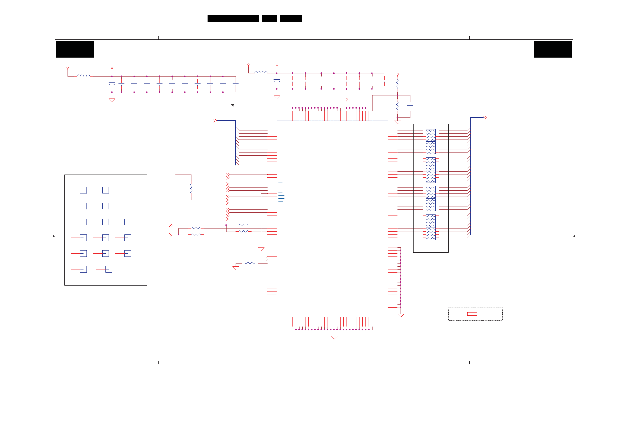
Circuit Diagrams and PWB Layouts
27QCS1.0S LA 7.
Scaler Board: DDR-SDRAM
5
S-A07 S-A07
2.5V_MEM
L15
KHB0805R121SA
D D
SCALER BOARD:
DDR_Q2.5V
C192
47uF/25V
C193
C194
0.1uF
0.1uF
+
C195
0.1uF
C196
0.1uF
DDR-SDRAM
C198
0.1uF
C199
0.1uF
AR[0..11]
C197
0.1uF
NeartoU30
MCLK-
MCLK+
150
R274
R691 0R
R309 0R
FIX1
C C
B B
FIX_MASK
FIX3
FIX_MASK
FIX5
FIX_MASK
FIX8
FIX_MASK
FIX11
FIX_MASK
FIX14
FIX_MASK
FIX2
FIX_MASK
FIX4
FIX_MASK
FIX6
FIX_MASK
FIX9
FIX_MASK
FIX12
FIX_MASK
FIX15
FIX_MASK
2007/03/02 Delete FIX15 a nd FIX16
FIX7
FIX_MASK
FIX10
FIX_MASK
FIX13
FIX_MASK
DQM0
DQM1
C200
0.1uF
4
+
A0
A1
A2
A3
A4
A5
A6
A7
A8/AP
A9
A10
A11
BA0
BA1
CK
CK
CKE
CS
RAS
CAS
WE
DQS0
DQS1
DQS2
DQS3
DM0
DM1
DM2
DM3
RFU1
RFU2
MCL
NC1
NC2
NC3
NC4
NC5
NC6
NC7
NC8
NC9
2007/02/28
C184
0.1uF
DDR_Q2.5V
C3
Q
VDD
VDDQC5VDDQC7VDDQ
VSSE5VSSE7VSSE8VSS
C201
0.1uF
SBA0
SBA1
MCLKMCLK+
CKE
RAS
CAS
WE
DQS0
DQS2
DQS1
DQS3
2.5V_MEM
C202
0.1uF
AR0
AR1
AR2
AR3
AR4
AR5
AR6
AR7
AR8
AR9
AR10
AR11
R690 0R
R692 0R
R310
NC(0R-MST)
DDR_Q2.5V
L124
KHB0805R121SA
C183
47uF/25v
N10
N11
M12
M11
N12
H13
B13
H12
B12
M10
M13
C11
H11
L12
L13
N5
N6
M6
N7
N8
M9
N9
M8
L6
M7
N4
M5
N2
M2
L2
L3
B2
H2
B3
H3
L9
C4
H4
M3
M4
N3
3
C186
C185
0.1uF
C10
C12
E3
C8
Q
VDD
VDDQ
M13S128324A-5BG_FPGA_144P
VSS
VSS
F6
F7
E10
0.1uF
2007/02/28
2
1
E1
F4
F1
G4
Q
Q
VDD
VDDQ
VDD
VDDQ
VSSF8VSSF9VSSG6VSSG7VSS
G8
Q
VDD
C187
0.1uF
1
G1
J4
VDDQ
U30
VSS
H6
G9
1
J1
VDDQ
VSS
H7
C188
0.1uF
DDR_Q2.5V
K11
K4
Q
VDD
VDDQ
VDDQ
VSS
VSS
VSS
H9
H8
D7
VSS
J6
C189
0.1uF
E4
E11
D
D
VD
VDDD8VD
VSSJ7VSSJ8VSSJ9VSS
K6
C190
0.1uF
L8
L4
D
VDD
VD
VDDL7VD
VSSK7VSSK8VSSK9VSSL5VSS
2
C191
0.1uF
DDR_Q2.5V
R306
1K
C182
R307
1K
0.1uF
L11
N13
D
VDD
VREF
DQ0
DQ1
DQ2
DQ3
DQ4
DQ5
DQ6
DQ7
DQ8
DQ9
DQ10
DQ11
DQ12
DQ13
DQ14
DQ15
DQ16
DQ17
DQ18
DQ19
DQ20
DQ21
DQ22
DQ23
DQ24
DQ25
DQ26
DQ27
DQ28
DQ29
DQ30
DQ31
VSSQ
VSSQ
VSSQ
VSSQ
VSSQ
VSSQ
VSSQ
VSSQ
VSSQ
VSSQ
VSSQ
VSSQ
VSSQ
VSSQ
VSSQ
VSSQ
VSSQ
VSSQ
VSSQ
VSSQ
L10
FSDATA 0
B7
FSDATA 1
C6
FSDATA 2
B6
FSDATA 3
B5
FSDATA4
C2
D3
D2
E2
K13
K12
J13
J12
G13
G12
F13
F12
F3
F2
G3
G2
J3
J2
K2
K3
2007/02/27
E13
D13
D12
C13
B10
B9
C9
B8
B4
B11
D4
D5
D6
D9
D10
D11
E6
E9
F5
F10
G5
G10
H5
H10
J5
J10
K5
K10
RS2
FSDATA 5
FSDATA 6
FSDATA 7
FSDATA16
FSDATA17
FSDATA18
FSDATA19
FSDATA20
FSDATA21
FSDATA22
FSDATA23
FSDATA8 M D ATA 8
FSDATA9
FSDATA10
FSDATA 11
FSDATA12
FSDATA13
FSDATA14
FSDATA15
FSDATA24
RS7
FSDATA25
FSDATA26
FSDATA27
RS8
FSDATA28
FSDATA29
FSDATA30
FSDATA31
4 5
3
2
1
4 5
3
2
33
1
RS3
4 5
3
33
2
1
4 5
RS4
3
33
2
1
4 5
RS5
3
2
33
1
4 5
RS6
3
33
2
1
4 5
3
2
33
1
4 5
3
33
2
1
RS1
33
M D ATA 0
M D ATA 1
6
M D ATA 2
7
M D ATA 3
8
M D ATA 4
M D ATA 5
6
M D ATA 6
7
M D ATA 7
8
MDATA16
MDATA17
6
MDATA18
7
MDATA19
8
MDATA20
MDATA21
6
MDATA22
7
MDATA23
8
M D ATA 9
6
MDATA10
7
M D ATA 1 1
8
MDATA12
MDATA13
6
MDATA14
7
MDATA15
8
MDATA24
MDATA25
6
MDATA26
7
MDATA27
8
MDATA28
MDATA29
6
MDATA30
7
MDATA31
8
2.5V_MEM
MDATA[0..3 1]
0228_EC
2.5V_MEM 2
1
I_17540_024.eps
5
4
3
2
1
310108
Page 28
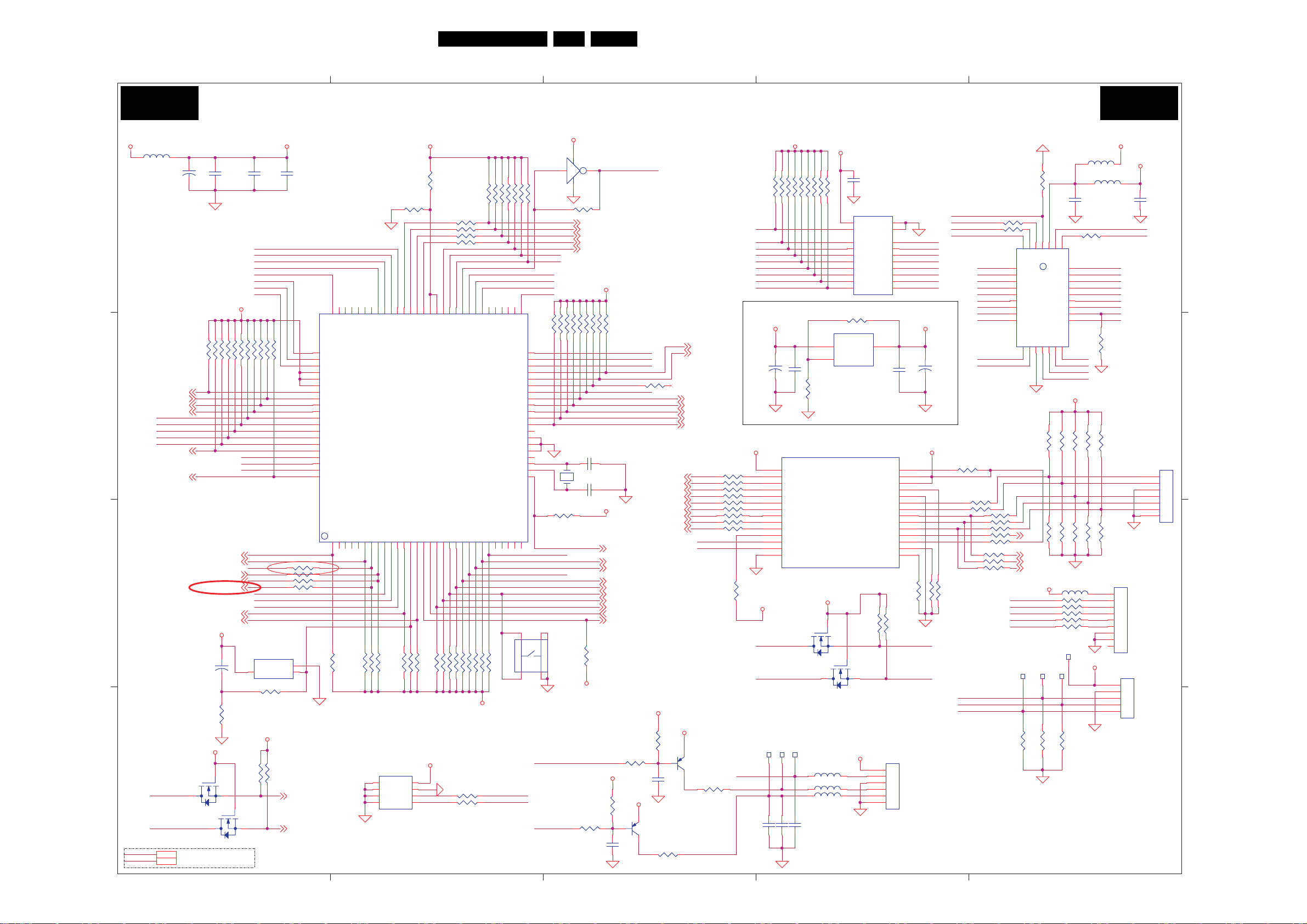
Circuit Diagrams and PWB Layouts
28QCS1.0S LA 7.
Scaler Board: MCU
5
S-A08 S-A08
L38
KHB0805R121SA
C203
47uF/25V
D D
PWR_OFF
SELFD_PPWR
C C
B B
A A
+3.3V_SW
+5VS
TCK
TMS
TDI
TD0
TRST
SCALER_AD2
SCALER_ALE
2007/06/04 Modify by Kodi
MSTR_SCL
MSTR_SDA
SCALER BOARD:
MCUVCC+5VS
1
+
2
PPWR
PBIAS
WINBOND_W79E659A40FL_QFP_100P
C451
2200uF/16V
Q49
2N7002
3
+3.3V_SW 2,4,10,11,15,16
+5VS 2,3,4,6,10,11
2
2
1
1
R349 10K
R350 10K
SCALER_RD
SCALER_WR
SELFD_INV
AMP_SD
S0
DDC_WP
SMT
MCUVCC
R396
0R
+3.3V_SW
2
3
Q50
2N7002
C204
0.1uF
MCUVCC
2
2
2
2
NC
1
1
1
1
R353
R352 NC
R351 NC
R355 NC
R354 NC
MCUA15
MCUA16
MCUA17
MTM_PST443A420NR
+
3
2
1
7
R41
1
2
1
5
C205
0.1uF
AD7
AD6
AD5
AD4
AD3
AD2
AD0 MCUA3
2
2
2
2
2
10K
1
1
1
1
1
R359 10K
R356 10K
R357
R358 10K
U34
R365 0R/NC
MCUA18
R382 0R/NC
1 2
R386NC
1 2
R388 JP/0603
1 2
KEY_ADC1
KEY_ADC2
KEY_ADC3
U37
GND
VDD
VOUT
R723 NC
+3.3V_SW
2
4.7K
1
12
2
4.7K
R418
1
3V3_SCL
3V3_SDA
C206
0.1uF
1
2
100
81
P0.2_AD2
82
P0.1_AD1
83
P0.0_AD0
84
VDD
85
VDD
86
VDD
87
P7.4
88
P7.5
89
P7.6
90
P7.7
91
TCK
92
TMS
93
TDI
94
TDO
95
TRST
96
P4.2
97
P1.0_PWM0_T2
98
P1.1_PWM1_T2EX
99
P1.2_PWM2_STADC
P1.3_PWM3
MCURESET
MCU
74
79
77
78
80
NC21
NC1976NC1875NC17
NC22
NC20
P0.3_AD3
NC45P1.5_PWM5_ADC1
P1.4_PWM4_ADC01NC12NC23NC3
4
7
6
10K
10K
1
1
7
2
R39
1
8
2
2
R399 10K
R39
ATM_AT 24C64A_SOIC_8P
1
2
3
1 2
72
70
P0.6_AD671P0.7_AD7
P0.4_AD473P0.5_AD5
P1.6_ADC2
P5.1_ADC5
P1.7_ADC38P5.0_ADC4
9
11
10
1
2
R400 10K
U38
A0
VCC
A1
A2
SCL
GND4SDA
P5.2_ADC6
R401 10K
WP
MCUVCC
R329
NC
69
66
67
68
L2
SC
P6.6_
P6.5_SDA1
P6.7_SDA2
ADC7
RST13P5.414P5.515P5.616P5.7
P5.3_
12
10K
1
1
1
2
2
2
2
R403 10K
R40
MCUVCC
8
7
6
5
4
1
2
R311 0R
R33147
R333 47
R33547
R33747
65
63
64
61
62
E
AL
P4.1
/EA1
/EA2
SCL1
P6.4_
D
P3.0_RX
P4.319P3.1_T
18
17
20
10K
1
1
1
1
5
2
2
2
2
R404 10K
R406 10K
R407 10K
R40
R421 100
R422 100
4
/PSEN
D
X
60
1
8 10K
2
R40
2
P2.7_A15_SDA
P3.2_/INT021P3.3
12
12
12
12
57
58
59
1
DA
P2.6_A14_SCL2
P2.5_A13_S
_/INT1
P3.4_T0
22
23
24
10K
1
1
1
0
2
2
2
R409 NC
R41
R411 10K
MCUVCC
12
12
1
1
R323 NC
R322 NC
2
2
55
CL1
NC1656NC15
P2.4_A12_S
T1
/WR
P3.5_
P3.6_
25
26
10K
1
2
2
R41
MSTR_SCL
MSTR_SDA
NC
1
1
1
1
R324
R325 NC
2
2
2
2
R326 10K
R327 10K
51
53
54
52
NC14
NC12
NC13
P2.2_A10
P2.1_A9
P2.0_A8
P6.3
P6.2
P6.1
P6.0
P7.3
P7.2
P7.1
P7.0
P4.0
NC11
VSS
VSS
VSS
NC10
XTAL1
XTAL2
P3.7_/RD
NC5
NC6
NC829NC9
NC7
28
27
30
2
1
SW1
SW_HCH_S TSB5
1
R330NC
2
R328 10K
ALE
PSEN
MCUA14
MCUA13
MCUA12
MCUA11
1
10K
8
2
P2.3_A11
R33
50
49
48
47
46
45
44
43
42
41
40
39
38
37
36
35
34
33
32
31
R372 10K
1 2
WR
MSTR_SDA
MSTR_SCL
IR_DATA
4
2
4
1
3
3
RED_CTL
GREEN_CTL
MCUVCC
2
1
1
10K
2
R339
U31
NC7SZ04P5X_SC70_5P
5
+
4
-
3
1 2
CE_SDA
CE_SCL
VGA_SDA
VGA_SCL
SCALER_AD1
MCUVCC
1
1
1
1
1
1
1
10K
10K
10K
2
2
2
2
2
2
2
R341
R340
R346 10K
R343
R345 10K
R342 10K
R344 10K
RED_CTL
GREEN_CTL
C214 22pF
X2
24.576MHz
C215 22pF
MCUVCC
2007/06/04 Modify by Kodi
APCCE_SW
MSTR_SDA
MSTR_SCL
SCALER_INT
TXD
SCALER_AD3
RXD
S1
AV _ SYNC
CSYNC_S EL
2
R731
10K
1
MCUVCC
MCUVCC
1
R423
NC
R424
4.7K
2
12
C220
0.1uF
3
ROM_CE
MCUA10
MCUA9
MCUA8
R360 NC
HDMI_SEL
BPCCE_SW
BPHD_CRL
ANAP_SD
EC_0606_CSYNC
Ctrl pi n
modification
MCUVCC
3
R41
NC
R419
4.7K
12
6
C21
0.1uF
MCUVCC
Q51
MMBT3906
1
2
3
R425 470
1 2
3
RGB_SEL
APHD_CRL
HWRESET
RESETN
MUTE
STBY
SCALER_AD0
2007/04/12 HDMI control
R363 0R
R364 0R
R366 0R
R367 NC
RPEAK1
RPEAK2
RPEAK3
GPEAK1
GPEAK2
1
MCUVCC
2
2
R368 0R
R370 0R
R373 0R
R375 0R
R377 0R
SB3V3_SDA
SB3V3_SCL
Q48
MMBT3906
1
3
R420 470
1 2
2
ALE
AD7
AD6
AD5
AD4
AD3
AD2
AD1
AD0AD1
MCUVCC
C210
470uF/16V
2
1
R313 NC
NC
+
MCUVCC
NC
2
2
1
1
R314
C212
0.1uF
NC
NC
2
1
R316
R315
1
2
2
1
NC
2
1
R317
NC
NC
2
2
1
1
R318
R319
R361
330/1%
NC
R320
3
1
MCUVCC
2
1
R321
TC74ACT373FT
20
11
17
13
7
3
R347200/1%
U35
VOUT
VIN
ADJ/GND
AIC1084/TO263
0.1uF
C207
U32
OE#
VCC
GND
LE
D718Q7
D6
D514Q5
D4
D38Q3
D2
D14Q1
D0
2
1
10
MCUA7
19
MCUA6
16
Q6
MCUA5
15
MCUA4
12
Q4
MCUA3
9
MCUA2
6
Q2
MCUA1
5
MCUA0
2
Q0
MCUVCC_3V3
2
C213
+
C211
220uF/35V
0.1uF
1
Near To U(F75101R)
MCUVCC_3V3 MCUVCC_3V3
R389
10K
MCUVCC_3V3
IR_DATA
LED_R
LED_G
U36
1
VSB3V
2
GPIO10/WD
3
GPIO11/LED
4
GPIO12/RQ
5
VIDIN0/GPIO16
6
VIDIN1/GPIO17
7
VIDIN2/GPIO20
8
VIDIN3/GPIO21
9
VIDIN4/GPIO22
10
VIDIN5/GPIO14
11
GPIO13/GP_ADDR
12
GP_DATA
13
GP_CLK
14
GND
F75101R
MSTR_SCL
MSTR_SDA SB3 V3_SDA
TP11
TP12
F
0.1u
8
C21
C217 0.1uF
2007/03/07 change the package
MCUVCC_3V3
Q46
2N7002
TP13
F
0.1u
C219
2
3
1
3
Q47
2N7002
SLOTOCC#
VIDOUT0/GPIO23
VIDOUT1/GPIO24
VIDOUT2/GPIO25
VIDOUT3/GPIO26
VIDOUT4/GPIO27
VIDOUT5/GPIO15
FUNC_SEL
VIDPWRGD
RSTOUT#
R394
2
1
MCUVCC
L410R
12
L420R
12
L430R
12
2
VBAT
VDD3V
VCCVID
GND
2
2
4.7K
1
1
EIC_4500-E06N
6
5
4
3
2
1
CN12
28
27
26
25
24
23
22
21
20
19
18
17
16
15
R383
10K
4.7K
R395
SB3V3_SCL
R38410K
MCUA18
R3320R
MCUA16
R3340R
MCUA15
MCUA12
MCUA7
MCUA6
MCUA5
MCUA4
MCUA2
MCUA1
MCUA0
AD0
AD1
AD2
R362 1M
R369 0R
R371 0R
R374 NC
R376 NC
R378 NC
R379 0R
R380 10K
R724 0R
R725 0R
R726 0R
2007/06/04 Modify by Kodi
R385
10K
KEY_ADC3
KEY_ADC2
KEY_ADC1
2007/04/12 L125/NC
0R
1
2
R312
12
12
2
3
4
1
5
6
2
8
A1
A1
A1
A1
5
A7
6
A6
7
A5
8
A4
U33
9
A3
10
A2
11
A1
12
A0
13
DQ13
DQ215VSS16DQ317DQ418DQ5
DQ1
7_
14
7_
GPEAK3
BPEAK1
BPEAK2
BPEAK3
MCUVCC
TRST
TD0
TDI
TMS
TCK
TP9
TP8
2
2
NC
R414 NC
1
1
R415
1
MCUVCC_3V3
L125
KHB0805R121SA/NC
L39
KHB0805R121SA
C208
0.1uF
R3360R
31
30
32
7
#
A1
VCC
WE
A14
A13
A8
A9
A11
OE#
A10
CE#
DQ7
DQ6
19
20
+3.3V_SW
2
2
NC
1
1
R707 NC
R706
2
2
1
1
R712 NC
R711 NC
KHB0805R121SA
R38747
1 2
R390 47
1 2
R391 47
1 2
R392 47
1 2
R393 47
1 2
TP7
TP10
2
R416 NC
1
12
EON_EN29F040A_70TIP_PLCC-32P
MCUA14
29
MCUA13
28
MCUA8
27
MCUA9
26
MCUA11
25
PSEN
24
MCUA10
23
ROM_CE
22
21
AD6
AD5
AD4
AD3
2
1
2
1
MCUVCC
1
L40
AD7
2
R348
1
2
2
NC
1
1
R710 NC
R708 NC
R709
FRAME_CTL
OS_CTL
TEMP3
TEMP2
TEMP1
2
2
NC
NC
4
5
1
1
R71
R713 NC
R71
1
2
3
4
5
6
7
8
9
EIC_4606-09
CN10
5
4
3
2
1
7_
MCUVCC
WR
MCUA17
NC
CON7/NC
1
2
3
4
5
6
7
8
9
EIC_4500-E05N
CN11
I_17540_025.eps
0.1uF
C209
J5
1
2
3
4
5
6
7
310108
Page 29
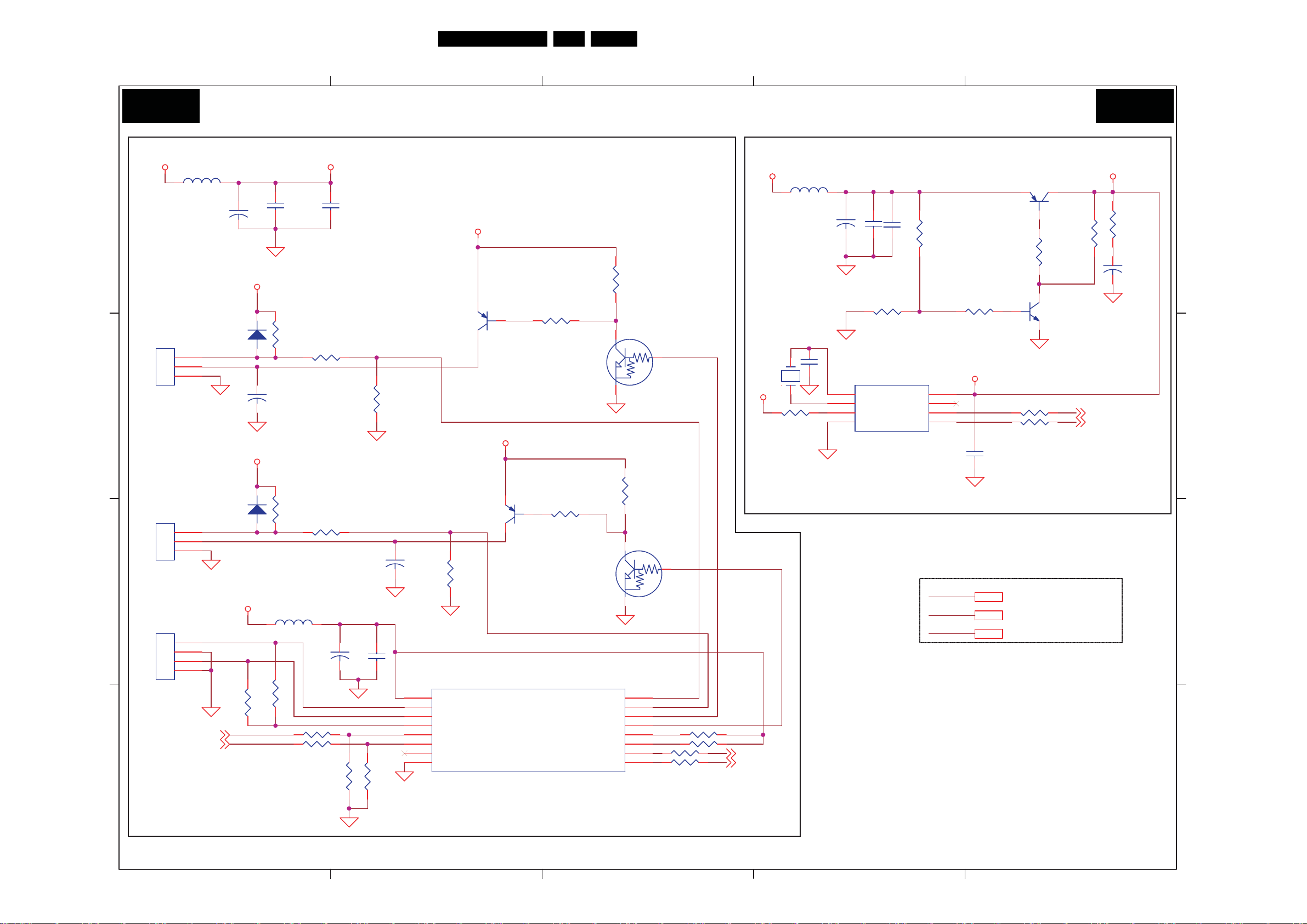
Circuit Diagrams and PWB Layouts
Scaler Board: Fan Control-RTC
5
29QCS1.0S LA 7.
4
3
2
1
S-A09 S-A09
D D
EIC_4500-E03N/NC
C C
B B
A A
CN13
EIC_4500-E03N/NC
CN14
4500-E04N/NC
CN15
SELFD_INV
SELFD_PPWR
SCALER BOARD:
L45
KHB0805R121SA/NC
1
C226
47uF/25V/NC
3
2
1
3
2
1
4
3
2
1
+
2
D34
1N4148/NC
D35
1N4148/NC
+3.3V_SW
R442 10K
FANVCC
1
2
FANVCC
1
2
1
2
C221
0.1uF
2
2
R432
4.7K
1
1
1
+
C228
47uF/25V/NC
2
2
2
R439
4.7K
1
1
R443 10K
2
R440 27K
1
L46 KHB0805R121SA/NC
R444 NC
R446 NC
FANVCC+12V_SW
R433
27K
1
C23
47uF/25V/NC
R450
4.7K
FAN CONTROL-RTC
C222
0.1uF
12
12
C230
47uF/25V/NC
1
2
+
C23
2
12
12
1
2
APM3195P/NC
FAN_DET1 FAN_CTL1
2
R434
10K
1
FAN_DET2
1
+
2
0.1uF
U40 F75375S/NC
16
15
14
13
12
11
1
R451
4.7K
2
10
9
FANVCC
Q54
3
2
Q56
APM3195P/NC
2
R441
10K
1
VCC
VT1
VT2
VREF
VIN1
VOLT_FAULT#/OVT#/GPIO3/EXT. CLOCK
VIN2
VIN3
GND
R646
1
0R
FANVCC
3
1
2
PWMOUT1/DACOUT1/ADDR_TRAP
PWMOUT2/DACOUT2/GPIO1
FAN_FAULT#/SMI#/GPIO2
12
R647
0R
12
FANIN1
FANIN2/GPIO0
SCLK
SD ATA
2
R431
4.7K
1
3
2
2
1
3
2
1
2
3
4
5
6
7
8
2007/04/14 pin define modify
1
Q55
DTC144E/NC
R438
4.7K
1
Q57
DTC144E/NC
FAN_DET1
FAN_DET2
FAN_CTL1
FAN_CTL2
R445 4.7K
R447 4.7K
R448 100
R449 100
+5VS RTCVCC
Pin2 change to Pin4
Hz
Y1
32.768k
RTCVCC
R43510K
FAN_CTL2
12
12
12
3V3_SCL
12
3V3_SDA
L44
KHB0805R121SA
+
47uF/25V
C223
C470
18pF
12
1
2
C224 0.1uF
R430
4.7K
U39
PHP_PFC8563T_TSSOP_8P
1
OSCI
2
OSCO
3
/INT
4
VSS
1uF
C225 0.
12
VDD
CLKOUT
SCL
SDA
1
R429
12K
2
8
7
6
5
C229
0.1uF
+3.3V_SW
+5VS
+12V_SW
R697
1 2
1K
RTCVCC
R436 33
R437
Q52
MMBT3906
2
+3.3V_SW 2,4,9,11,15,16
+5VS 2,3,4,6,10,11
+12V_SW 2,6,11,12,14
2
1
2
3
1
33
31
R426
12K
R428
33K
Q53
MMBT3904
12
12
1
2
MSTR_SCL
MSTR_SDA
1
2
1
+
2
R427
560
C227
1F_5.5V
I_17540_026.eps
310108
5
4
3
2
1
Page 30
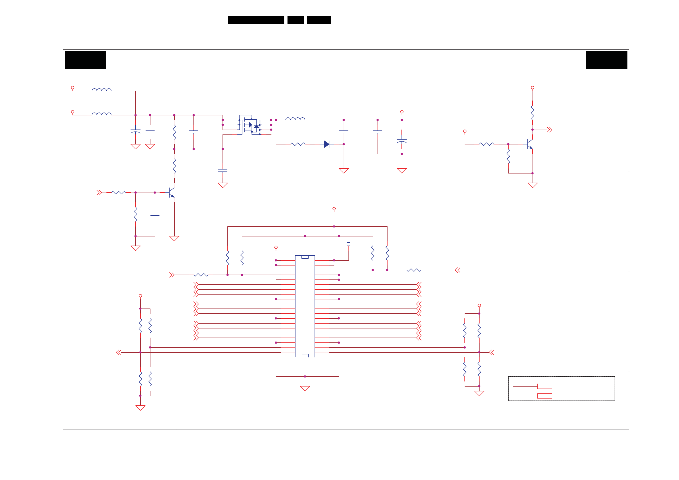
Circuit Diagrams and PWB Layouts
Scaler Board: Panel Interface
5 4 3 2 1
30QCS1.0S LA 7.
S-A10 S-A10
+12V_SW
D
+5V_SW
C
KHB0805R121SA
KHB0805R121SA/NC
PPWR
SCALER BOARD:
L47
L48
1
1
2
C233
0.1uF
1
2
C440
100uF/25V
R458
1 2
4.7K
R459
1M
+
2
1
2
1
2
1
2
3
2
1
C238
0.1uF
PANEL INTERFACE
1
R453
10K
2
R457
2.2K
Q60
MMBT3904
C234
2200pF
2
3
4 5
1
C441
0.1uF
2
Q58
SI9435
+5V_SW
PANEL_POWER
L49
81
7
6
220 OHM
R454
1 2
2.2K/NC
12
D36
SML-310/NC
PANEL_POWER
1
C235
0.1uF/NC
2
1
2
C236
0.1uF
1
+
2
C237
100uF/25V
PANEL_POWER
R455 22K
1 2
1
R456
2K
2
2
R452
10K
1
3
2
1
SELFD_PPWR
Q59
MMBT3904
D
C
TP14
R659
0R
RL_L
SELLVDS
IP1
R657
0R
UD_D
PANEL_POWER
1
3
5
7
9
11
13
15
17
19
21
23
25
27
29
31
33
35
37
39
CN16
42
44
2
4
6
8
10
12
14
16
18
20
22
24
26
28
30
32
34
36
38
40
41
43
EIC_3950_F40C_00R_40P
2
2
R656
NC
R658
NC
UD_HULD
+3.3V_SW
B
2
2
R460
NC
VBR_OUT
R466
0R
R461
NC
1
1
2
2
R467
0R
1
1
1 2
TXA3+
TXAC+
TXA2+
TXA1+
TXA0+
TXB3+
TXBC+
TXB2+
TXB1+
TXB0+
1
1
A
2
2
R660
NC
1
1
R661
NC
12
TXA3-
TXACTXA2-
TXA1TXA0TXB3-
TXBCTXB2TXB1TXB0-
R462
NC
R464
0R
RL_HRLL
+3.3V_SW
2
2
1
1
2
2
1
1
R463
NC
R465
0R
EXT_VBR
+3.3V_SW
+12V_SW
+3.3V_SW 2,4,9,10,15,16
+12V_SW 2,6,10,12,14
B
A
I_17540_027.eps
310108
Page 31
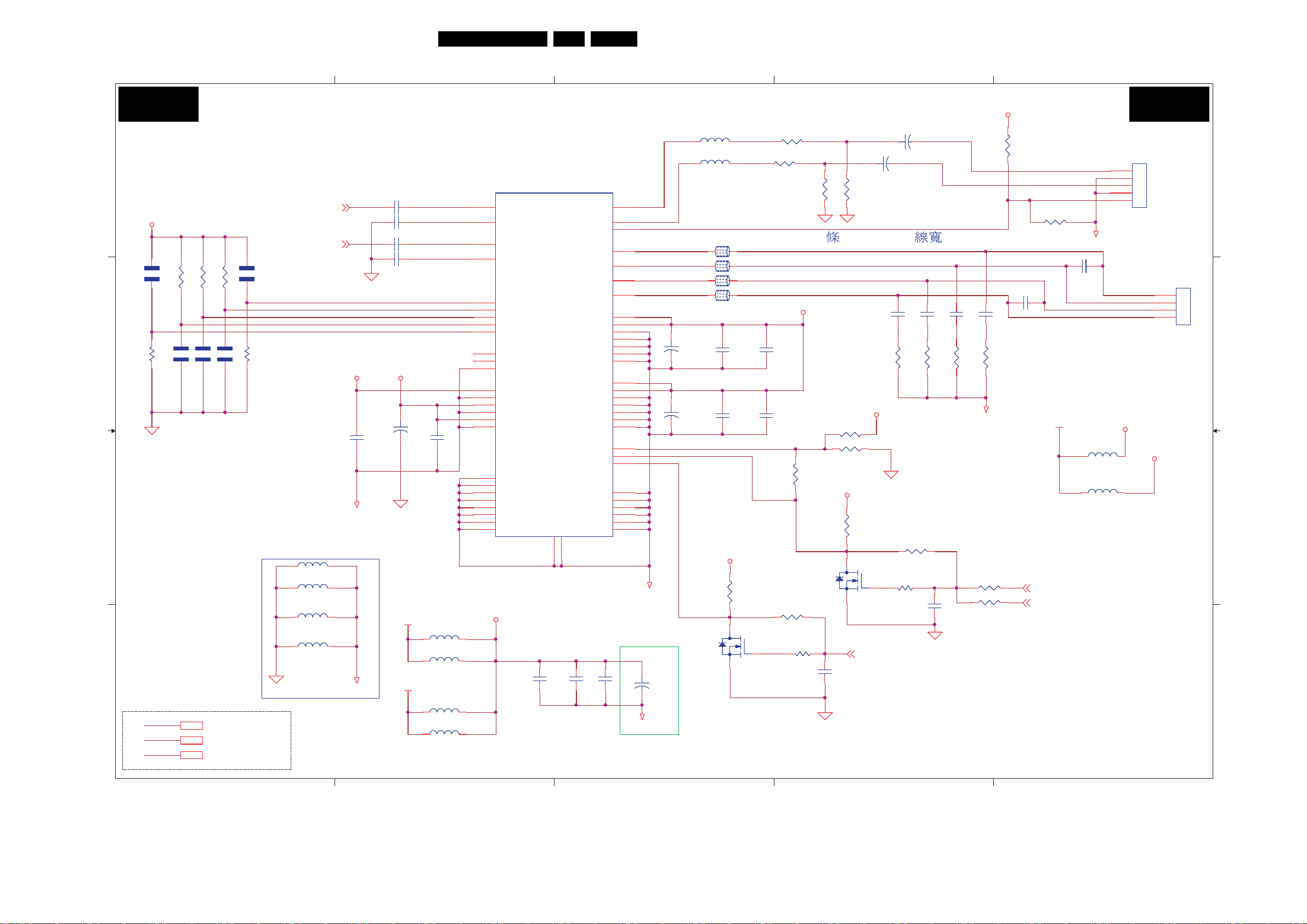
Circuit Diagrams and PWB Layouts
31QCS1.0S LA 7.
Scaler Board: Audio Amplifier
5
S-A11 S-A11
D D
+5V_REF
2
R471NC
1
C C
R476
75
B B
A A
+5V_SW
+12VA
+12V_SW
SCALER BOARD:
R47210K
R477NC/6
2
1
R47410K
R47310K
2
8
R47
1
NC/6
+5V_SW2
+12VA 2
+12V_SW 2,6,10,11,14
R479NC/6
2
475
R
1
NC/6
2
1
5
R480
75
L52
KHB0805R121SA
L54
KHB0805R121SA
L57
KHB0805R121SA
L60
KHB0805R121SA
AUDIO_L
AUDI O_R
C257
0.1uF
AUDIO AMPLIFIER
C2391uF
1 2
C241 1uF
1 2
C243 1u F
1 2
C244 1u F
1 2
+12V_AMP
AGND
AGND
+5V_REF
258
+
1
2
C
0.1uF
10uF/50V
+12VA
+12V_SW
4
38
39
A-OUT_R29
1
C259
2
5
4
27
26
25
24
23
19
20
21
40
3
41
2
22
18
43
44
45
46
47
48
49
50
+12V_AMP
L55 KHB0805R121SA
L58 KHB0805R121SA
L61 KHB0805R121SA/NC
L62 KHB0805R121SA/NC
4
U41
YDA138
INL
VREFL
INR
VREFR
VOL1
VOL0
MODE2
MODE1
MODE0
CKIO
XO
X1
PVDDREG
VSSBGR
REFA
AVSS
DVD D
DVSS
THERMAL1
THERMAL2
THERMAL3
THERMAL4
THERMAL5
THERMAL6
THERMAL7
THERMAL8
C262
0.01uF
3
2
1
+5V_REF
C240 10uF/50V
+
+
C247
1
R482
2.2/8
2
H : NORMAL
L:PROTECT
R489
1 2
NC
2
R491
75/NC
2
2490.01uF
C
C248
01uF
0.
1
1
R483
R484
2.2/8
1
2
C260
0.1uF
2.2/8
2
AGND
R492 0R
1 2
1 2
R493 NC
2
C252
0.1uF
C255
0.1uF
1
2
Q62
3
1
R673 1K
1 2
R674 1K
1 2
+12V_AMP
1
C253
0.1uF
2
1
C256
0.1uF
2
R494
1 2
2N7002
NC
2
C242 10uF/50V CN17
1
1
R675
100K
R676
100K
2
2
4 OUT LINE :40mil
0.01uF
R481
2.2/8
+5VB1
R485
2K
12
+5VB1
1
2
3
1
12
Q61
2N7002/NC
MUTE
2
R487
22
1
R495
75
R486NC
R488 3.3K
1
C261
0.1uF
2
L108 0R
1 2
L109 0R
1 2
HPL_29A-OUT_L29
42
HPOL
HPOR
HP
OUTPL
OUTML
OUTPR
OUTMR
PVDDPL
PVDDML
PVSSL
PVSSL
PVSSL
PVSSL
PVSSL
PVDDPR
PVDDMR
PVSSR
PVSSR
PVSSR
PVSSR
PVSSR
PROTN
SLEEPN
MUTEN
THERMAL16
THERMAL15
THERMAL14
THERMAL13
THERMAL12
THERMAL11
THERMAL9
THERMAL10
52
51
0.01uF
1
2
1
C263
2
0.01uF
1
2
C264
HPR_29
1
37
A_SPEAKER_1+
35
A_SPEAKER_1-
29
A_SPEAKER_2+
8
A_SPEAKER_2-
14
36
28
30
31
32
33
34
7
15
9
10
11
12
13
16
17
6
58
57
56
55
54
53
AGND
AGND
1
C265
+
1000uF/16V
2
FB1 BCRH127
FB2 BCRH127
FB3 BCRH127
FB4 BCRH127
1
+
C251
100uF/25V
2
1
+
C254
100uF/25V
2
3
HP_138
1 2
1 2
1 2
1 2
1
2
1
2
+5V_REF
R490
3.3K
2
HeadPh one Jack
HPL
HPR
AGND
C245
0.22uF/NC
SPKLO+
SPKLO-
SPKRO-
5
4
3
2
1
EIC_4500-E05N/NC
SPKRO+
C250
0.01uF
1
R468
NC
1
C246
0.22uF/NC
R762 0R
1 2
SPEAKER OUTPUT
2
+5V_SW
KHB0805R121SA
S-AMP_SLEEP
H:AMPPower Savin g ( D efault )
L : N ORMALOPERATION
PWR_OFF
AMP_SD
S-AMP_MUTE
H : AMP OFF (Default)
L : N ORMALOPERATION
+5VB1
+5V_REF
FB5
L50
KHB0805R121SA
1
CN18
4
3
2
1
EIC_4606-04
I_17540_028.eps
310108
Page 32
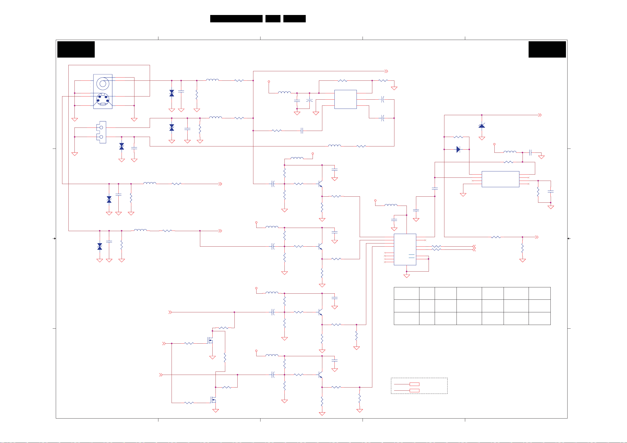
Circuit Diagrams and PWB Layouts
32QCS1.0S LA 7.
Scaler Board: Board Diagram
5
S-A12 S-A12
D D
A
V_CIN
CBNC2P-YKC31-0184ON6_0
C C
SCALER BOARD:
JACK1
6 7
8
11
10
5
1
3
TYCO_1566504_4_5P
P1
P2
J1
P1
EZJZ0V800AA/NC
AV_CIN
EZJZ0V800AA/NC
D42
G1
G1
G2P2
D39
1
2
9
2
4
BNC_CVBS_IN
CVBS_OUT
1
2
C274
100pF
AV_YIN
C273
100pF
L68 0R
1 2
R506
75_1/2W
RCA_CVBS_IN
EZJZ0V800AA/NC
EZJZ0V800AA/NC
BOARD SCHEMATIC DIAGRAM
1
C266
D37
D38
R505 0R
100pF
2
1
C271
100pF
2
4
L63 0R
1 2
R499
75_1/2W
L65 0R
1 2
R501
75_1/2W/NC
2007/04/12 For CVBS InputLevel
R496 0R
R500 0R
SCIN
+5VSB
+5V_VD
L64
KHB0805R121SA
R502 10
C277
+
1 2
47uF/25V
L71
C267
22uF/50V
C269
0.1uF
C272
0.1uF
CVBS_OUT
L67
KHB0805R121SA
R507
10K
R509
100
R510
15K
1
+
2
+5VSB
3
2
R497 47K
6
VCC
5
GND
4
IN
L66 0R
3
Q63
MMBT3904
R511
1
680
R513
1.8K
U42
PS
OUT
SAG
MM1671
R503 75_1/2W
12
C275
0.1uF
1
2
3
R498 NC
C268
100uF/25V
1 2
C270
47uF/25V
1 2
+5VSB
CVBSIN
+
+
L72
KHB0805R121SA
C283
0.1uF
2
1
D40
UDZ5V6B
2
+5VSB
KHB0805R121SA
U43
1
CVBS_SYNC_OUT
2
CVBS_IN
3
V_SYNC_OUT
4
GND
NS_LM1881_SOP_8P
C278
0.47uF
C280
470pF
R504
1.1K
D41
2 1
1SS355
L69
R508 560K
VCC
OD/EVN
RSET
BRST/BK
1
AV _ SYNC
C276
0.1uF
8
7
6
5
R514
560K
C281
0.1uF
L70 0R
1 2
1
D43
EZJZ0V800AA/NC
B B
A A
C279
R515
100pF
2
5
75_1/2W
BNC_H_CSYNC
R512 0R
EC_0608
DSUB_H_CSYNC
CSYNC_S EL
R749
75_1/2W
Q78
2SK3018
R752
1K
Q79
2SK3018
R753
EC_0606_CSYNC
1K
4
SYIN
R751
75_1/2W
R750
0R/NC
+5VSB
+5VSB
KHB0805R121SA
C284
+
1 2
47uF/25V
L127
KHB0805R121SA
C479
+
1 2
47uF/25V
L128
KHB0805R121SA
C481
+
1 2
47uF/25V
R520
15K
R736
15K
R741
15K
R517
10K
R734
10K
R739
10K
R519
100
R735
100
R740
100
C282
Q64
MMBT3904
R521
680
R522
1.8K
Q76
MMBT3904
R737680
R518
1.8K
Q77
MMBT3904
R523
1.8K
0.1uF
C286
0.1uF
C285
0.1uF
R742
680
R746
2.2K/NC
R747
2.2K/NC
3
2
1
3
2
1
3
2
1
3
5
4
3
10
11
12
13
CSYNC_SEL
RGB_SEL
16
1B161A
1B2
1B3
1B4
2B1
2B2
2B3
2B4
8
Control
Pins
+5VSB
+5V_VD
U44
PI5V331QE
2A
VCC
S0
S1
1OE
2OE
GND
2
7
9
R7320R
1 2
14
R733 0R
1 2
2
1
15
EC_0606_CSYNC
CVBS
L
L
+5VSB 2,5,6
+5V_VD 2,14,17
S-VIDEO
L
H
CSYNC
RGB_DSUB
H
L
R516 0R
RGB_SEL
CSYNC_S EL
CSYNC
RGB_BNC
H
H
R738
NC
EC_0606_CSYNC
HV
RGB_DSUB
L
L
1
CSYNC_H
HV
RGB_BNC
L
H
I_17540_029.eps
310108
Page 33
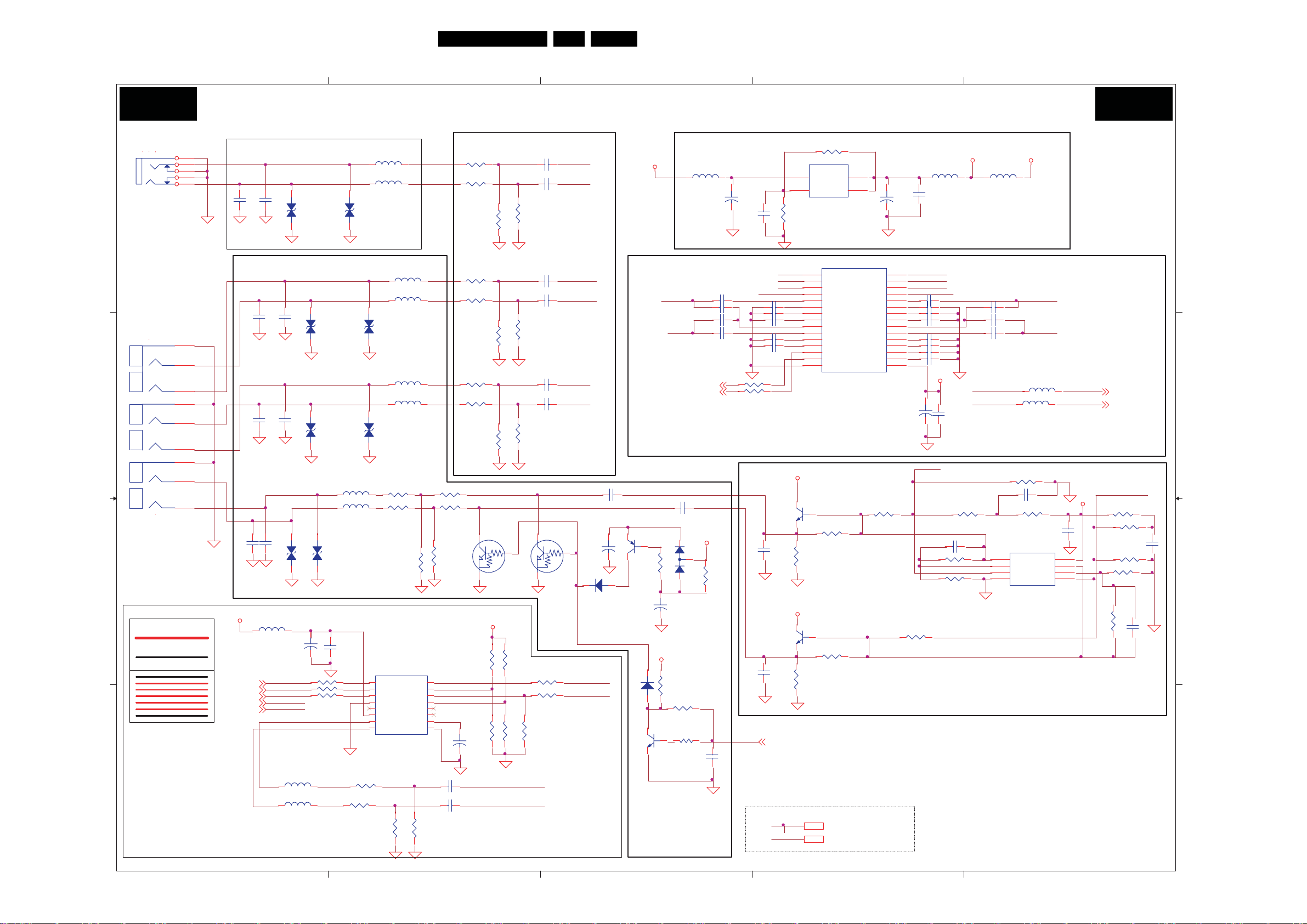
Circuit Diagrams and PWB Layouts
Scaler Board: Audio Input
5
33QCS1.0S LA 7.
4
3
2
1
S-A13 S-A13
8
7
6
PHONEJACK STEREO
JACK2
D D
SCALER BOARD:
1
2
4
5
3
NeartoJACK2
C294
100pF
1
D46
EZJZ0V800AA/NC
2
C293
100pF
NeartoJACK3
C303
100pF
C315
100pF
1
2
C324
10uF/50V
5_
AUS CK
5_
AUSD
5_
AUW S
AUMCLK
AUM UTE
1
D48
EZJZ0V800AA/NC
2
1
D50
EZJZ0V800AA/NC
2
1
0AA/NC
D52
80
2
EZJZ0V
+
R558 0R
1 2
R560 0R
1 2
R561 0R
1 2
HDMI_L
HDMI_R
JACK3
SINGA_2PJ_246V_B18_9P
10
1
F
C
C C
E
B
D
A
B B
3
2
4
6
5
7
9
8
11
Signal Lines
C302
100pF
C314
100pF
MONIA_R
MONIA_L
C320 100pF
+5V_VD
L86
KHB0805R121SA
pF
C321 100
GND
AUSCK
AUSD
AUW S
AUM CLK
AUM UTE
A A
5
L870R
1 2
L88 0R
1 2
AUDIO INPUT
L73
0R
1 2
L77 0R
1 2
1
D47
EZJZ0V800AA/NC
2
L78
0R
1 2
L79 0R
1 2
1
D49
EZJZ0V800AA/NC
2
L80
0R
1 2
L810R
1 2
1
D51
EZJZ0V800AA/NC
2
L84
0R
1 2
L850R
1 2
3
0AA/NC
D5
80
EZJZ0V
C325
0.1uF
R566 1K
1 2
R567 1K
1 2
R542
0R
1 2
1 2
R543
0R
R545
100K
U47
1
BCK
2
DATA
3
LRCK
4
DGND
5
NC
6
VCC
7
VOUTL
VOUTR8AGND
TI_PCM1754_SSOP_16P
R678
100K
1
2
SCK
FMT
MUTE
DEMP
TEST
ZEROA
VCOM
1
2
R693 1K
1 2
R694 1K
1 2
1
1
R544
100K
2
2
16
15
14
13
12
11
10
9
C329 1u F
C3301uF
R677
100K
4
R525
1K
1 2
1 2
R526
1K
100K
R530
1K
1 2
1 2
R531
1K
100K
R537
1K
1 2
1 2
R539
1K
R541
100K
3
2
R552
0uF/50V
+
C328 1
NC
R563 0R
1
R529
2
1
R535
2
1
2
Q72
DTC144E/NC
+5V_VD
2
2
1
1
2
2
1
1
HDMIOPT_LIN
HDMIOPT_RIN
1
R564
1
2
1
2
1
2
R553
0R
Near to U46
1uF
1 2
1 2
1uF
R527
100K
1uF
1 2
1 2
1uF
R534
100K
1uF
1 2
1 2
1uF
R540
100K
3
2
NC
1 2
1 2
R562 NC
2
0R
R565
1
C288
PC_LIN
PC_RIN
C289
C296
AV 1 _ R IN
AV1_LIN
C297
C310
AV 2 _ R IN
AV2_LIN
C312
Near
to
U46
C318 1uF
1
Q73
DTC144E/NC
R559
0R
C452
D60
AUMC LK
AUM UTE
1 2
+
/25V
00uF
1
1N4148/NC
12
+12V_SW
C319 1uF
Q74
MMBT3906
1
2
1
3
47K
R698
2
7uF/25V
C453 4
A9VOUT
C
1
2
2
1
D61 1N4148/N
3
1
Q75
MMBT3904/NC
3
L74
MONIAR
OUTa
MSTR_SCL
MSTR_SDA
1 2
2
1
+
R699
3.3K
R700
1 2
NC
R701
2
75
KHB0805R121SA
C290
470uF/16V
C322 1uF
C444 NC
C446 NC
C316 1uF
A9VOUT
3
1
27K
D59 BAV99
2
R705
1
0.1uF
2
C454
+
C295
0.1uF
PC_RIN
AV1_RIN
AV2_RIN
HDMIOPT_RIN
C471 22 00pF/NC
C298 2200pF
C300 0.1uF
C304 1uF
C306 1uF
R536100
1 2
R538 100
1 2
A9VOUT
C326
470pF
A9VOUT
C327
470pF
MUTE
+5V_VD
+12V_SW
R524
120/1%
U45
3
VIN
1
ADJ/GND
AP1117ELA/TO223
R528
750/1%
U46
1
IN1a
2
IN2a
3
IN3a
4
IN4a
5
MONa
6
NC1
7
TONE-Ha
8
TONE-La
9
LINEa
10
OUTa
11
CVa
12
CVb
13
SDA
14
SCL
15
GND
Q65
MMBT3904/NC
3
AMP_ROUT
2
1
1 2
1
R555
NC
2
Q66
3
MMBT3904/NC
2
1
R556 0R
1 2
1
R557
NC
2
+5V_VD 2,13,17
+12V_SW 2,6,10,11,12
2
VOUT
4
OUT
JRC_NJW1141M_SDMP_30P
R532
0R
AMP_LOUT
IN1b
IN2b
IN3b
IN4b
MONb
NC2
TONE-Hb
TONE-Lb
LINEb
OUTb
AGC
CTH
CTL
Vref
2
V+
R549
0R/NC
C291
+
10uF/50V
30
29
28
27
26
25
24
23
22
21
20
19
18
17
16
100uF/25V
12
1 2
L75
KHB0805R121SA
C292
0.1uF
NeartoU46
PC_LIN
AV1 _LI N
AV2 _LI N
HDMIOPT_LIN
C323 1 uF
C472 22 00pF/NC
C299 2200pF
C301 0.1u F
C305 0.33uF
C307 1uF
C308 1uF
C309 1uF
A9V
C311
+
C313
0.1uF
MONIAR
C474 33pF
R652 15K
1 2
R654 47K
1 2
R548
0R/NC
A9V
C445 NC
C447 NC
C317 1uF
R650
47K
L76
KHB0805R121SA
OUTa
L83 0R
OUTb
12
1 2
R651 27K
C473 1u F
R717 100K
1 2
1
OUTA
2
INA1
3
INA2
VSS4INB2
U55
TS482IDT/SOIC8
A9VOUT
Near to U41
MONIAL
OUTb
L820R
1 2
12
A9V
C448
0.1uF
8
VCC
7
OUTB
6
INB1
5
1
AUDIO_R
AUDI O_L
MONIAL
R551 100K
1 2
R655 47K
C475
1uF
R653 27K
R550 47K
12
1
2
R716 15K
C476 33pF
Nearto
U46
I_17540_030.eps
12
12
310108
Page 34
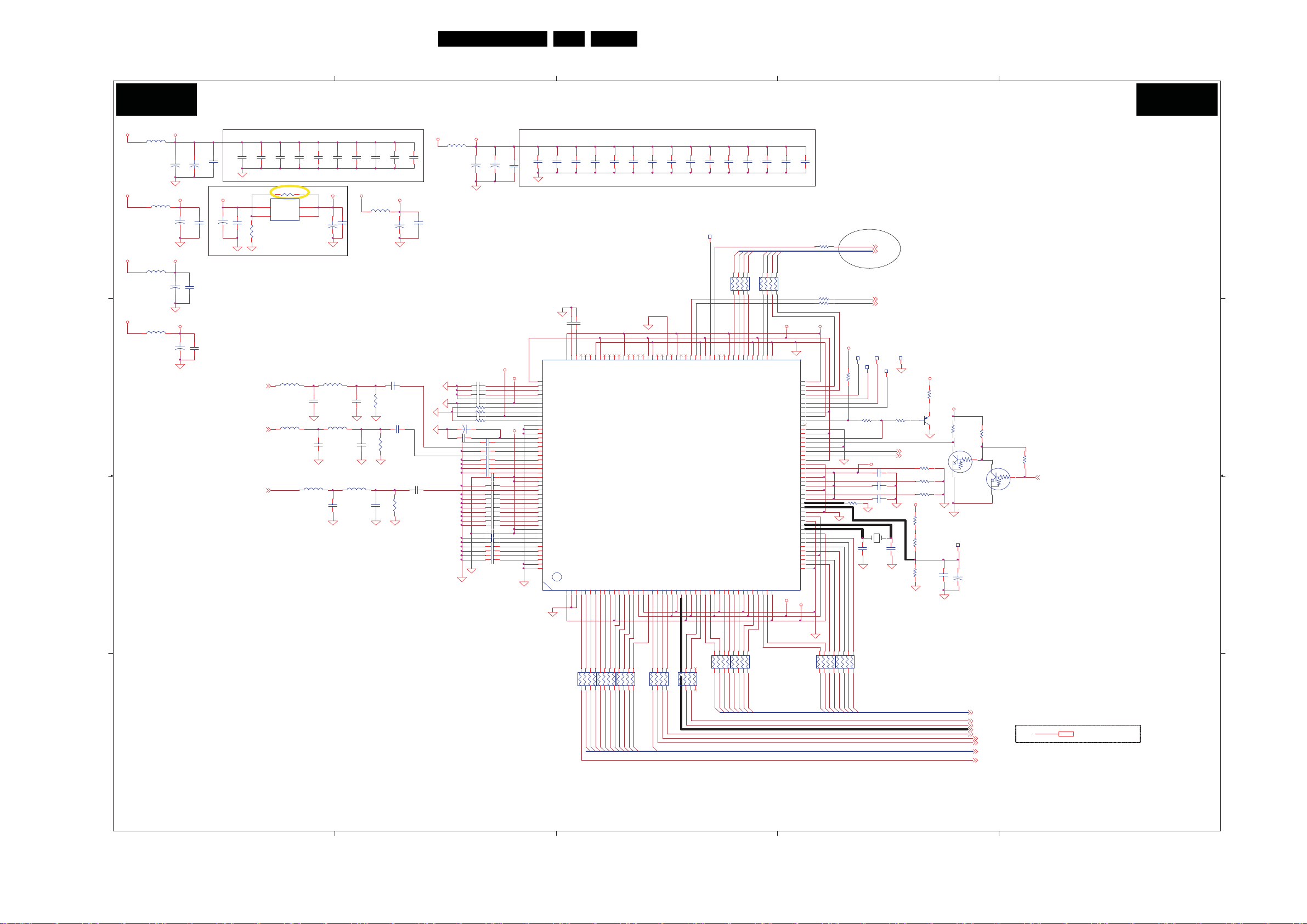
Circuit Diagrams and PWB Layouts
34QCS1.0S LA 7.
Scaler Board: Video Decoder
S-A14 S-A14
L89
KHB0805R121SA
KHB0805R121SA
L93
KHB0805R121SA
KHB0805R121SA
+3.3VD
1
C419
2
+3.3VA O
C418
+3.3VA
1
C413
2
VDEC+3.3V
C415
V
+
22uF/50
C420
1
+
22uF/50V
2
1
+
2uF/50V
2
2
1
+
22uF/50V
2
+3.3V_SW
+3.3V_SW
D D
+3.3V_SW
L91
+3.3V_SW
L94
C C
B B
5
SCALER BOARD:
pin1, 11, 26, 44, 53, 88,98, 109, 120, 132
V
+
2
22uF/50
C408
2
1
0.1uF
2
C412
+3.3V_SW
+
331470uF/16V
C
0.1uF
0.1uF
2
C333 0.1uF
1
C400
C399
1
1
0.1uF
0.1uF
C442
1
0.1uF
2
C443
CVBSIN
1
1
C403
C407
0.1uF
0.1uF
2
2
R568 560/1%
3
VOUT
VIN
1
ADJ/GND
OUT
U48
AP1117ELA/TO223
R572
100/1%
NeartoU49
L95
270
L97
SYIN
270
SCIN
1
C343
0.1uF
2
2
4
C336
39pF/NC
C351
1.5pF/NC
L99
270
1
C345
0.1uF
2
+1.5VDD
C332
L96
0R
C358
39pF/NC
1
2
+
47uF/25V
C337
L98
0R
4
VIDEO DECODER
+1.5VDD +1.5VD
L90
C356
KHB0805R121SA
1
2
1
0.1uF
2
C411
C339 0.1uF
C350 0.1uF
C353 0.1uF
C354 0.1uF
C360 0.1uF
R578 47K
R58047K
C361 0.1uF
R58147K
C363 22uF/50V
C364 0.1uF
1 2
CVBS_AV1
SY_ASY1
SC_ASC1
C347
0.1uF
1
0.1uF
2
C409
68pF/NC
C352
3.3pF /NC
L100
0R
1
2
+1.5VDD
C359
C349
0.1uF
68pF/NC
1
C357
0.1uF
2
+1.5VA
L92
KHB0805R121SA
C334
0.022uF
R573
1K
0.022uF
R574
1K
1
2
C414
C340
C388
0.1uF
1
+
2
R577
1K
22uF/50V
0.022uF
1
+
C416
2
1 2
1 2
1 2
1 2
1 2
1 2
1 2
1 2
1 2
12
+
C366 0 .1uF
1 2
C367 0 .1uF
1 2
C368 0.1uF
1 2
C371 0 .1uF
1 2
C370 0 .1uF
1 2
C3800.1uF
1 2
C372 0 .1uF
C375 0 .1uF
C378 0.1uF
C3840.1uF
C3810.1uF
C374 0 .1uF
C3820.1uF
C3850.1uF
C383 0.1uF
C3860.1uF
C3870.1uF
C396 0 .1uF
C377 0 .1uF
C3890.1uF
C390 0 .1uF
C391 0 .1uF
C395 0.1 uF
22uF/50V
C417
1 2
1 2
1 2
1 2
1 2
1 2
1 2
1 2
1 2
1 2
1 2
1 2
1 2
1 2
1 2
1 2
1
+
22uF/50V
2
VDEC+3.3V
+3.3VA
12
3
pin16,23,27,32, 39, 48, 57, 70, 76, 8 1, 92, 103, 115, 125, 133
uF
C410 0.1
+1.5VA
1
2
C342
0.1uF
uPD64015
1
1
C344
0.1uF
2
2
C338
0.1uF
U49
133
DVDD1
134
DYMI
135
DCGI
136
DCBI
137
DCRI
138
AVDD1
139
ATS1
140
ATS2
141
AVDD3
142
ATS3
143
AGND
144
AGND
145
AGND
146
VCLY
147
VCOM1
148
AV I
149
VLPF1
150
ASYI*
151
VRB1
152
ACYI*
153
VRT1
154
ACSI*
155
AVDD3
156
AVDD3
157
VRT2
158
ASCI
159
VRB2
160
AGI
161
VCOM2
162
ACBI
163
VRT3
164
ABI
165
VRB3
166
VCOM3
167
AVDD3
168
AVDD3
169
VCOM4
170
ACRI
171
VLPF2
172
ARI
173
VRB4
174
VRT4
175
AGND
176
AGND
C346
0.1uF
132
2
1
131
DVDD 3
DVDD 31SCKSET2TES
1
2
2
1
130
DFBI
DYSI
T
3
C348
0.1uF
C335
0.1uF
129
127
128
FCSI
FCKQ
FOCP
SDRABP4SDRA115SDRA10
6
1
2
126
7
C341
0.1uF
125
DGND
SDRA9
123
124
FDIO9
DVDD 1
SDRA88SDRA79SDRA610DVD
1
C362
0.1uF
2
122
121
120
D3
FDIO7
FDIO8
FDIO6
DVD
A5
A4
D3
SDR
SDR
12
13
11
1
1
C369
C365
0.1uF
0.1uF
2
2
114
115
116
113
117
118
119
FDIO2
FDIO1
DGND
FDIO3
FDIO4
FDIO5
DVDD 1
uPD64015
A1
A0
CS
SDRA314SDRA215DVDD 116DGND17SDR
SDR
SDR
18
19
20
1
2
110
111
112
BCKM
FDIO0
SDRCKE21SDRRAS22DVDD 123DGND24SDR
C355
0.1uF
109
RDEO
108
DVDD 3
25
1
2
106
107
FILD
VBLK
CLK
DVDD 326DVDD 127SDRCAS28SDRWE
2
100
ROCK
1
2
VD0
8
10 100
123
RS
98
97
ROY199ROY0
DVDD 3
DQ6
SDRDQ935SDRDQ536SDRDQ10
34
C404
0.1uF
1
C405
0.1uF
2
VD3
VD2
VD1
6
7
5
4
94
93
5
ROY
ROY495ROY396ROY2
DGND38DVDD 1
37
39
VD4
RS9 100
123
92
91
DGND
DVDD 1
1
SDRDQ440SDRDQ1
SDRDQ342SDR
41
1
2
VD5
43
ROY790ROY6
DQ12
C406
0.1uF
VD6
678
89
44
VD7
5
4
+1.5VD
DGND
SDRDQ15
SDRDQ0
SDRDQ14
SDRDQ1
SDRDQ13
SDRDQ2
DVDD 3
+1.5VD
1
2
DVDD 3
ROY8
ROY9
ROY10
ROY11
ROY12
ROY13
DVDD 1
DGND
ROFDIE
FCLK8
FCKM
DVDD 1
RGRED
RSTB
SLA0
DVDD 1
AGNDA
IOCR
AVDDA
AGNDA
IOCB
AVDDA
AGNDA
IOYG
AVDDA
RSET
AGNDA
DVDD 1
DGND
DVDD 3
DVDD 1
DGND
SDA
C392
0.1uF
SCL
REF
VD_
HD_
XO
+3.3VD
1
2
R571 100
R569 100
R570 100
88
87
86
85
84
83
82
81
80
79
78
77
76
75
74
73
72
71
70
69
68
67
66
65
64
63
62
61
60
59
58
57
56
55
XI
54
53
52
51
50
49
48
47
46
45
1 2
1 2
1 2
+3.3VD
VD[0:7]
+3.3VD
TP36
1
2
R576 10K
R579 47K
R586 620
1 2
TP37
1 2
C373 0.1uF
1 2
C376
1 2
C379
1 2
REF_VIDEO
1 2
1
24.576MHz
C393
2
22pF
VLLC
VD[0:7]
SVS
SHS
TP38
+3.3VA O
2007/02/27
TP40
TP39
R5821K
1 2
0.1uF
0.1uF
X3
1
C394
2
22pF
Q67
MMBT3906
2
3V3_SDA
3V3_SCL
R589NC
R588 NC
R587NC
+3.3VA O
2
1
2
1
2
1
+3.3VD
R590
2.2K/1%
R591
100/1%
R592
1K/1%
C398
1
R575
1K
2
+3.3VD
1
1
1
R583
3
10K
R584
2
3
12
2
12
12
F
u
2
1
C397 0.1
10K
2
1
3
Q68
DTC144E
2
2007/04/18 R58 6change to 620R/0603/0.5%
TP41
1
+
22uF/50V
2
1
Q69
DTC144E
1
2
R585
10K/NC
RESETN
1
C401
C402
0.1uF
0.1uF
2
TP35
BCLK8
101
105
103
104
102
VD
HD
DGND
BCLK8
DVDD 1
SDRDQ831DVDD 132DGND33SDR
SDRDQ7
29
30
1
8
RS11
123
CLK
SDR
100
5
678
123
RS19
100
DQ8
4
SDRDQ7
CAS
SDR
SDR
SDRWE
RS18
5
567
8
567
8
RS15
100
RS16
100
A A
5
4
678
1
3
234
SDRA7
4
1
2
RS17
100
A4
A5
SDR
SDRA3
SDR
SDRA6
SDRA1
SDRA2
3
4
1
2
1
A9
A10
SDRA1
SDRA8
SDR
SDR
567
8
100
123
4
RCS
SDRA0
SD
SDRCKE
SDRRAS
3
RS12
100
123
4
4
10
DQ9
DQ11
DQ6
SDR
SDRDQ5
SDRDQ4
SDR
SDRDQ
SDR
SDRABP
RS13
100
8
1
SDRDQ3
SDRCKE
SDRCS
2
SDRDQ12
567
3
4
DQ13
SDRDQ2
SDR
123
DQ1
SDR
14
SDRDQ
5
678
4
SDRDQ0
SDRDQ15
RS14
100
2
SDRDQ[15..0]
SDRWE
SDRCAS
SDRCLK
SDRRAS
SDRA[11..0]
SDRDQ[15..0]
SDRWE
SDRCAS
SDRCLK
SDRRAS
SDRCKE
SDRCS
SDRA[11..0]
SDRABP
+3.3V_SW
+3.3V_SW 2,4,9,10,11,16
1
I_17540_031.eps
310108
567
8
567
Page 35
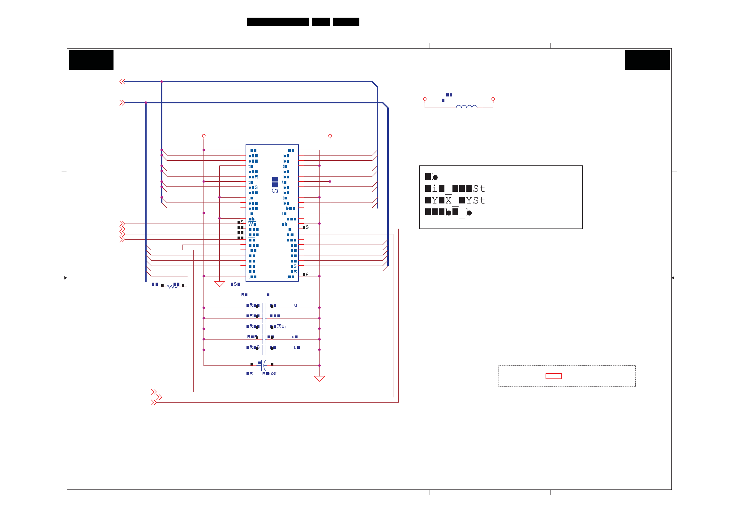
Circuit Diagrams and PWB Layouts
Scaler Board: Video Decoder SDRAM
5
35QCS1.0S LA 7.
4
3
2
1
S-A15 S-A15
SDRDQ[15..0]
SDRA[11..0]
D D
C C
SCALER BOARD:
DRDQ[15..0]
S
1..0]
SDRA[1
SDRWE
SDRCAS
SDRRAS
SDRCS
SDRA10
SDRA0
SDRA1
SDRA2
SDRA3
SDRA11
SDRDQ0
SDRDQ1
SDRDQ2
SDRDQ3
SDRDQ4
SDRDQ5
SDRDQ6
SDRDQ7
VIDEO DECODER SDRAM
SDRDQ[15..0]
SDRA[11..0]
SÉ
RÉ
RÉ
RÉ
RÉ
RS
RR
RÉ
RÉ
RÉ
RÉ
?É
?É
?É
ǐÉ
ƠR
?É
?É
?É
?É
?É
ưÉ
?É
+3.3V_DDR+3.3V_DDR
SDRDQ15
SDRDQ14
SDRDQ13
SDRDQ12
SDRDQ11
SDRDQ10
SDRDQ9
SDRDQ8
16MbitSDRAM
?
?
?
R
S
Ш
?
?
?
?É
?É
?É
?É
?R
ǘÉ
?É
?É
?É
?É
?R
?S
+3.3V_SW +3.3V_DDR
SDRA9
SDRA8
SDRA7
SDRA6
SDRA5
SDRA4
?É?É_ףּ
u
B B
+3.3V_SW
SDRABP
SDRCKE
SDRCLK
A A
+3.3V_SW 2,4,9,10,11,15,16
I_17540_032.eps
310108
5
4
3
2
1
Page 36
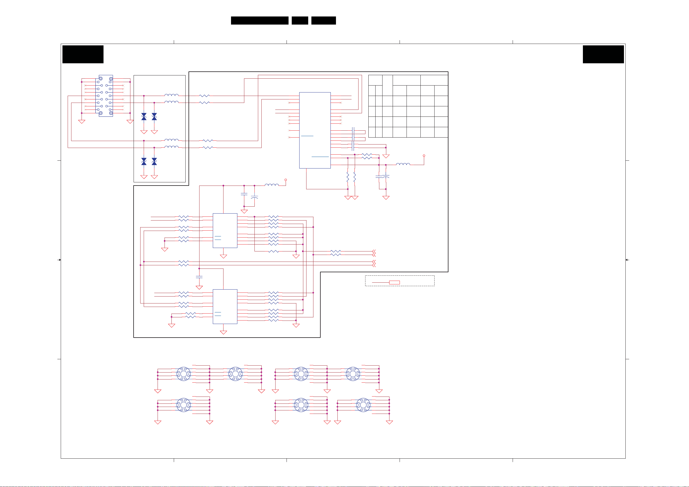
Circuit Diagrams and PWB Layouts
36QCS1.0S LA 7.
Scaler Board: RS232
5
S-A16 S-A16
TEKCON_1297_000_410_52_18P
D D
C C
B B
SCALER BOARD:
J2
G2G4
14
18
13
17
12
16
11
15
10 1
5
9
4
8
3
7
2
6
G1G3
EZJZ0V800AA/NC
EZJZ0V800AA/NC
D54
D56
NeartoJ2
L102 0R
L103 0R
1
2
L104 0R
L105 0R
1
2
1
D55
EZJZ0V800AA/NC
2
1 2
1 2
1
D57
EZJZ0V800AA/NC
2
TX1
RX1
TX2
RX2
R601 100
R695 0R
R606 100
R608 100
R610 0R
R612 0R
R617 100
R618 100
R619 100
R696 0R
R623 100
R625 100
12
12
1 2
1 2
1 2
1 2
1 2
1 2
1 2
1 2
C434
0.1uF
1 2
1 2
1 2
1 2
R627 0R
1 2
R629 0R
1 2
RS232
R59333
R594 33
R595 33
R596 33
12
12
1 2
1 2
7
9
14
2
1
15
1
2
7
9
14
2
1
15
4
RXD_OUT RXD_OUT
TXD_OUT
RXD_IN
TXD_IN
1
+
2
10uF/50V
6
5
4
3
10
11
12
13
6
5
4
3
10
11
12
13
U52
1A
2A
S0
S1
1OE
2OE
1A
2A
S0
S1
1OE
2OE
16
VCC
GND
PI5C3253
8
U53
PI5C3253
16
VCC
GND
8
C433
0.1uF
1B1
1B2
1B3
1B4
2B1
2B2
2B3
2B4
1B1
1B2
1B3
1B4
2B1
2B2
2B3
2B4
TXD_IN
TX2
RX1
L107
KHB0805R121SA
C450
R602 100
1 2
R603 100
1 2
R604 100
1 2
R607 100
1 2
R609 100
1 2
R611 100
1 2
R613 22K
1 2
R614 100
1 2
R605 NC
1 2
R620 NC
1 2
R621 100
1 2
R622 100
1 2
R624 22K
1 2
R626 100
1 2
R628 100
1 2
R630 100
1 2
R631 22K
1 2
MCUVCC
10
11
19
18
17
16
15
20
21
9
SP3243
T1OUT
T2OUT
T3OUT
R1OUT
R2OUT
R3OUT
R4OUT
R5OUT
R2OUTB
INVALID
U51
FORCEOFF
GND
25
T1IN
T2IN
T3IN
R1IN
R2IN
R3IN
R4IN
R5IN
C1+
C2+
FORCEON
VCC
14
13
12
4
5
6
7
8
28
24
C1-
1
2
C2-
27
V+
3
V-
23
22
26
R599
NC
R615 0R
1 2
R616 0R
1 2
3
RX2
TX1
TXD_OUT
RXD_IN
0.47uF/10V
C427
12
C428 0.1uF
12
C429 0.47uF/10V
1 2
C430 0.47uF/10V
1 2
1
1
R600
NC
2
2
Control
Pins
S1
L
L
H
H
R597100
R598100
C431
0.1uF
S0
L
H
L
H
12
12
1
2
RXD
TXD
S1
S0
MCUVCC
IN-terminal
MODE
TXD
RXD
Enable
0
1
2
NA
C449
+
10uF/50V
Enable Enable
Disable
Enable Enable Enable
Enable
XXXX
L106
KHB0805R121SA
MCUVCC 2,13,14
OUT-terminal
RXD TXD
Enable
MCUVCC
Disable
EnableEnable
2
1
S1
2
3
4
5 6
MTH315D138
S3
2
3
4
A A
5
5 6
MTH315D138
10
9
8
1
7
1
10
9
8
1
7
1
S2
2
3
1
4
5 6
MTH315D138
4
10
9
8
7
1
S4
2
3
1
4
5 6
MTH315D138
S6
2
3
1
4
5 6
MTH315D138
10
9
8
7
1
10
9
8
7
1
S5
2
3
1
4
5 6
MTH315D138
S7
2
3
4
5 6
MTH315D138
3
10
9
8
7
1
10
9
8
1
7
1
I_17540_033.eps
2
1
310108
Page 37
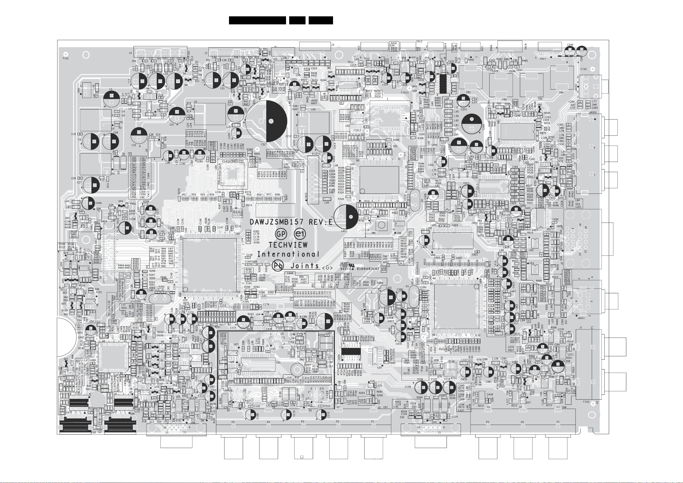
Circuit Diagrams and PWB Layouts
Layout Scaler Board (Top Side)
37QCS1.0S LA 7.
I_17540_034.eps
310108
Page 38
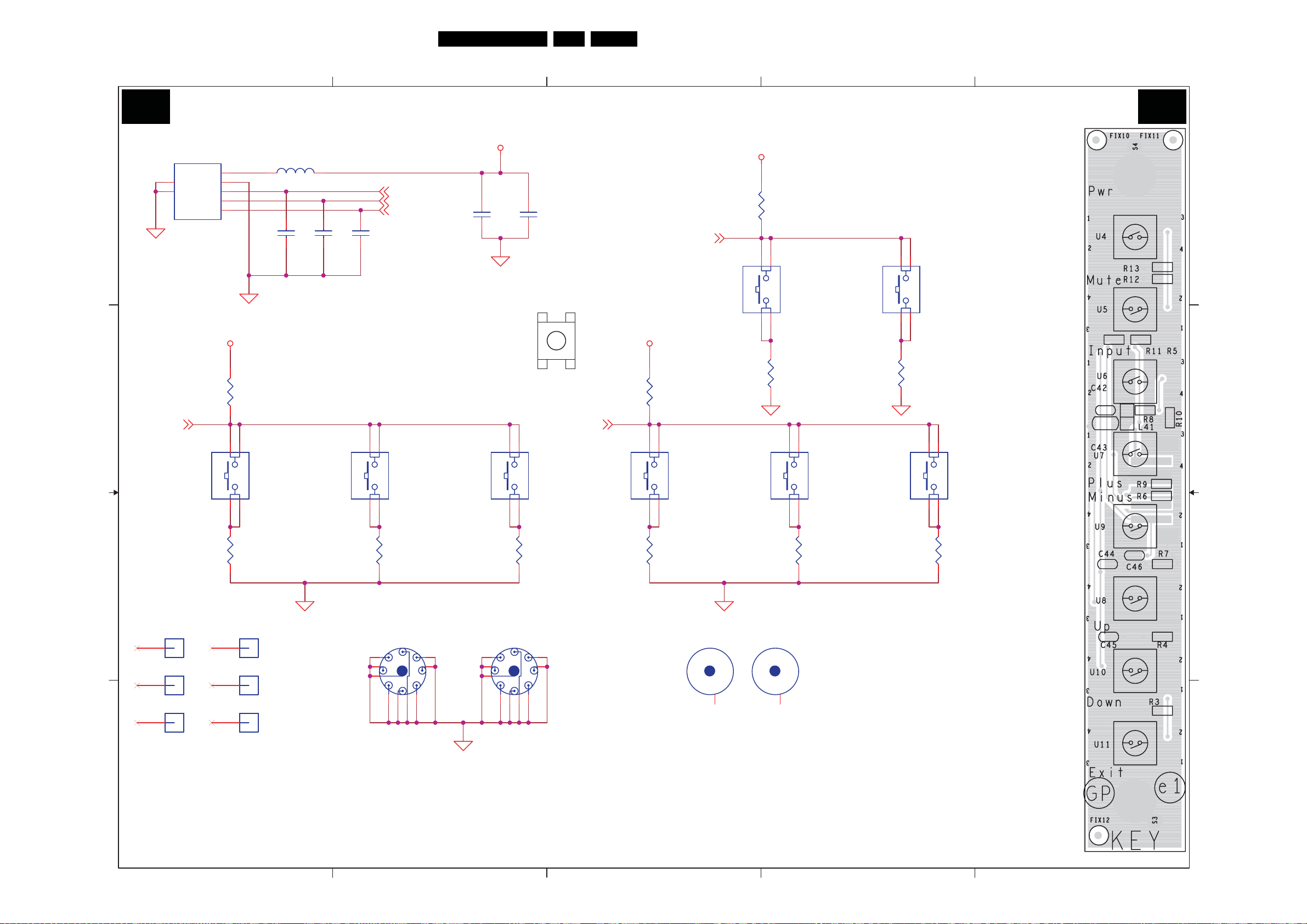
Keyboard Panel
Circuit Diagrams and PWB Layouts
5
38QCS1.0S LA 7.
4
3
2
1
B B
D D
KEYBOARD PANEL
CN8
6
G
7
G
SMD
EIC_4510_E05N
1
2
3
4
5
1
2
3
4
5
0.1uF
L41
KHB0805R121SA
C44
C45
0.1uF
C46
0.1uF
ADC_IN3
ADC_IN2
ADC_IN1
C42
0.1uF
KEY_5V
C43
1uF
ADC_IN1
U4
TOUCH SWITCH 4P
KEY_5V
1
R11
10K/1%/0603
3
TOUCH SWITCH 4P
U5
3
1
SMD SWITCH
PWR MUTE
4
2
KEY_5V KEY_5V
R13
R8
C C
10K/1%/0603
Package STSB5
R5
10K/1%/0603
0R
2
4
R12
4.7K
ADC_IN2 ADC_IN3
TOUCH SWITCH 4P
U6
3
1
TOUCH SWITCH 4P
U7
1
3
TOUCH SWITCH 4P
U8
3
1
TOUCH SWITCH 4P
U9
3
1
TOUCH SWITCH 4P
U10
1
3
TOUCH SWITCH 4P
U11
1
3
PLUSINPUT UP MINUS DOWN EXIT
2
2
4
R10
0R
B B
FIX10 FIX_MASK
FIX11 FIX_MASK
FIX12 FIX_MASK
FIX13 FIX_MASK
FIX14 FIX_MASK
FIX15 FIX_MASK
4
R9
4.7K
3
3
2
2
1
1
9
9
8
4
4
5
5
6
8
7
7
6
2
4
R7
20K
3
3
2
2
1
1
9
9
8
4
4
5
5
6
778
6
2
4
R6
0R
1
2
4
R4
4.7K
1
2
4
R3
20K
A A
I_17540_037.eps
5
4
3
2
1
310108
Page 39
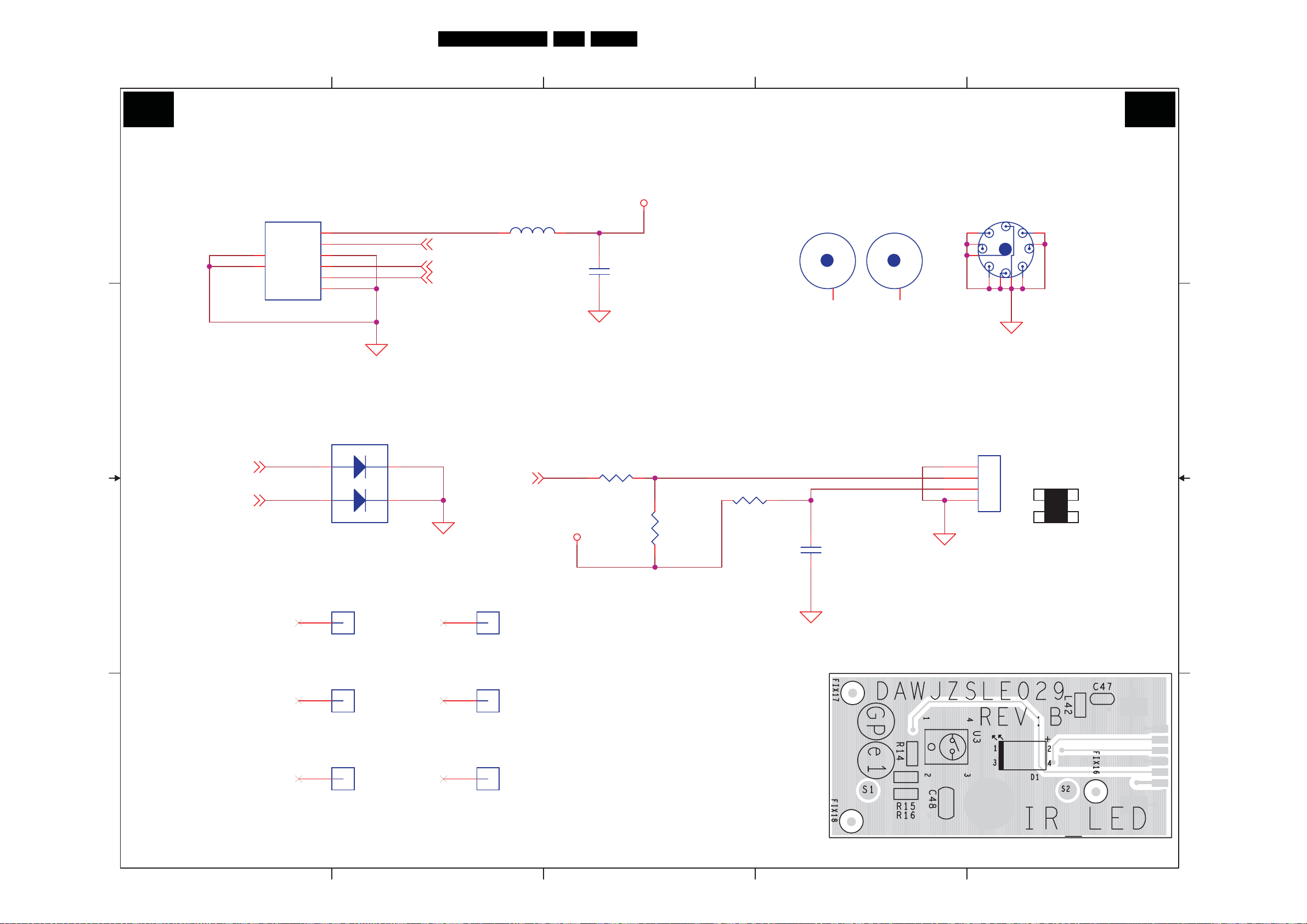
IR & LED Panel
Circuit Diagrams and PWB Layouts
5
39QCS1.0S LA 7.
4
3
2
1
L L
IR & LED PANEL
Part modified
D D
C C
CN9
3801_1.25pitch_6pin
SMD Connector
1
1
2
2
7
G
8
G
ROHM_SML020MLTT86
3
3
4
4
5
5
6
6
D1
IR_DATA
RED
GREEN
L42
1 2
JP/RC0603
REMO_V33
C47 0.1uF
3
3
2
2
1
1
1
1
U3
9
4
4
5
5
6677889
OPTO_FM_1040FN_F_5NR_REV_4P
RED
GREEN
2
4
1
3
MLTT86Package
IR_DATA
REMO_V33
R14 0R
R15
3.3K
R16 47
C48 10uF
1
2
3
4
2
3
1
4
SMD IR Sensor
Packag e : REV_4P
B B
FIX1
FIX_MASK
FIX2
FIX_MASK
FIX3
A A
FIX4
FIX_MASK
FIX5
FIX_MASK
FIX6
FIX_MASK
5
4
FIX_MASK
I_17540_039.eps
3
2
1
310108
Page 40
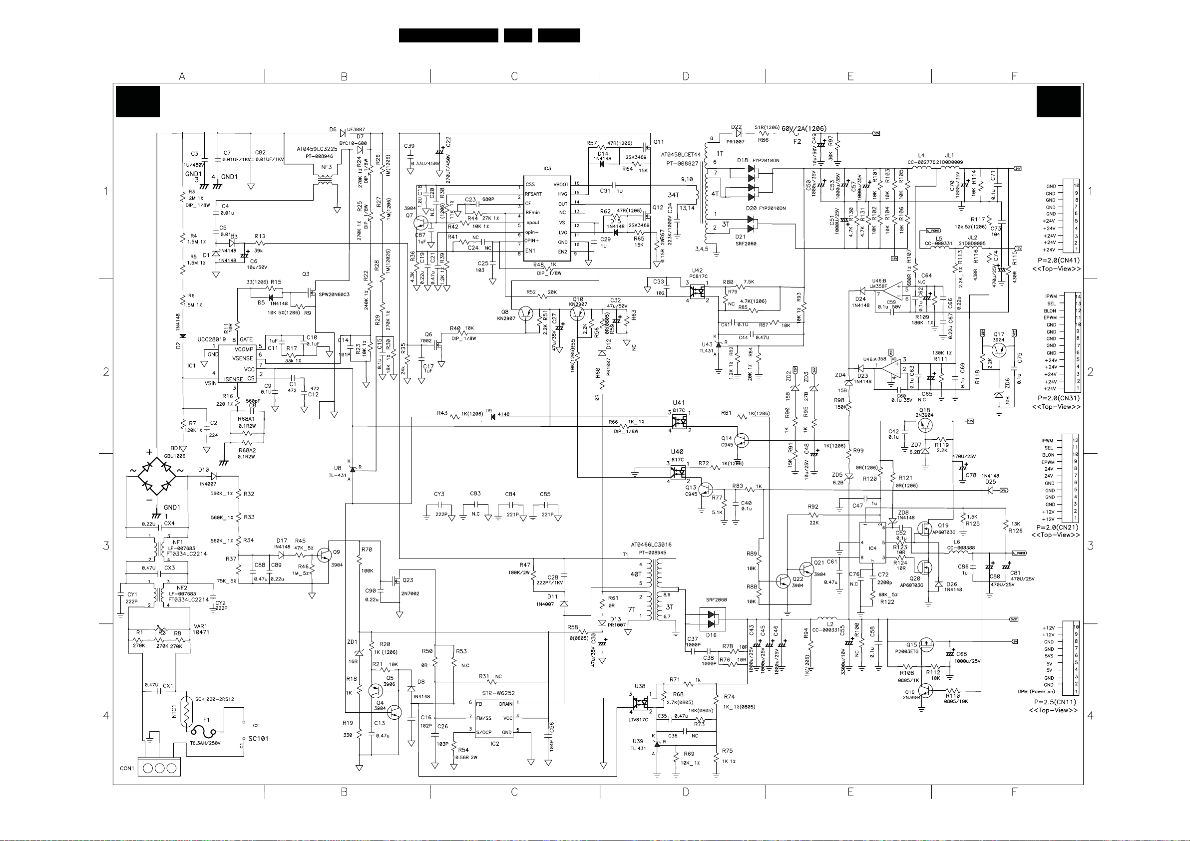
Power Board
Circuit Diagrams and PWB Layouts
40QCS1.0S LA 7.
P P
POWER BOARD
I_17540_041.eps
310108
Page 41
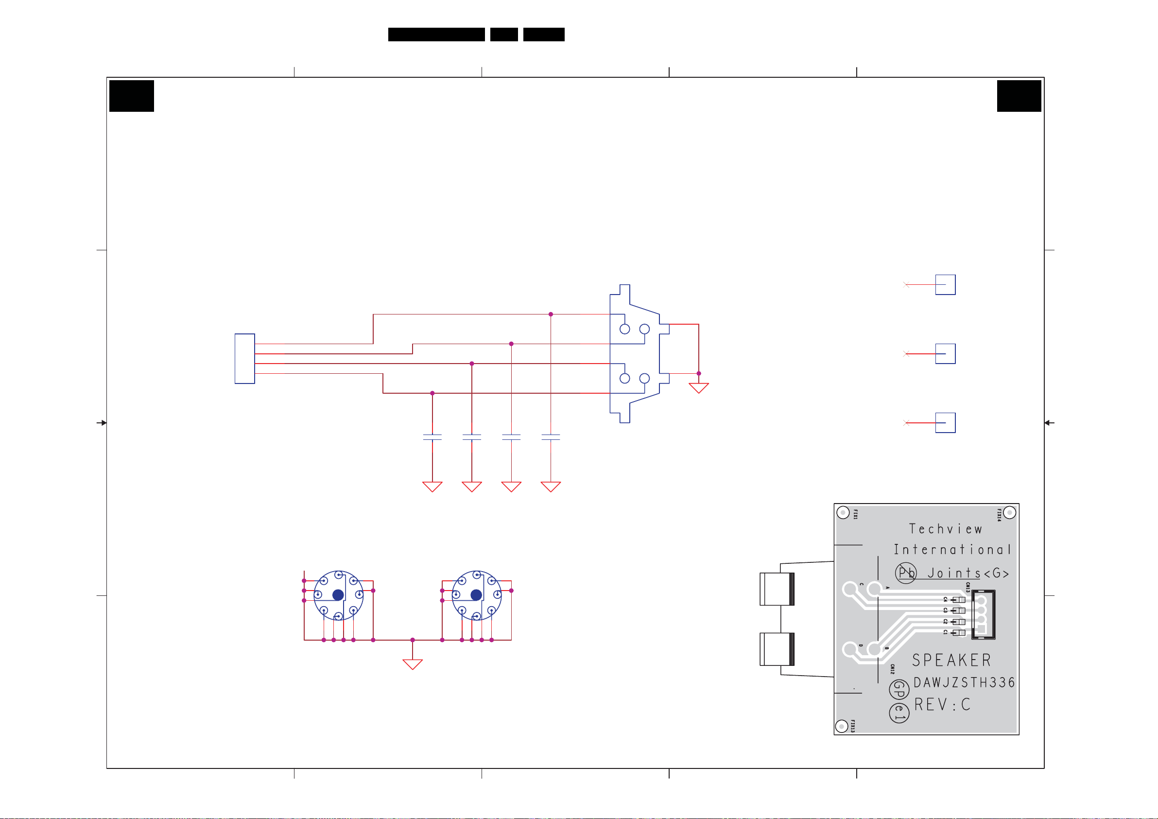
Speaker Board
Circuit Diagrams and PWB Layouts
5
41QCS1.0S LA 7.
4
3
2
1
SP SP
D D
SPEAKER BOARD
FIX16
CN12
FIX_MASK
1
A
C C
4
3
2
1
4500-E04N
CN13
ABC
3
C
2
B
D
4
D
5
G
FIX17
6
G
FIX_MASK
FIX18
TEKCON_5110-855-310-52_4P
C1
330pF
C2
330pFC3330pF
C4
330pF
DIP Packag e : 5110_4pin
FIX_MASK
B B
3
3
2
2
1
1
889
9
A A
5
4
4
5
5
7
6
7
6
4
3
3
2
2
1
1
9
4
4
5
5
6677889
I_17540_035.eps
3
2
1
310108
Page 42
Personal Notes:
Circuit Diagrams and PWB Layouts
42QCS1.0S LA 7.
E_06532_013.eps
131004
Page 43
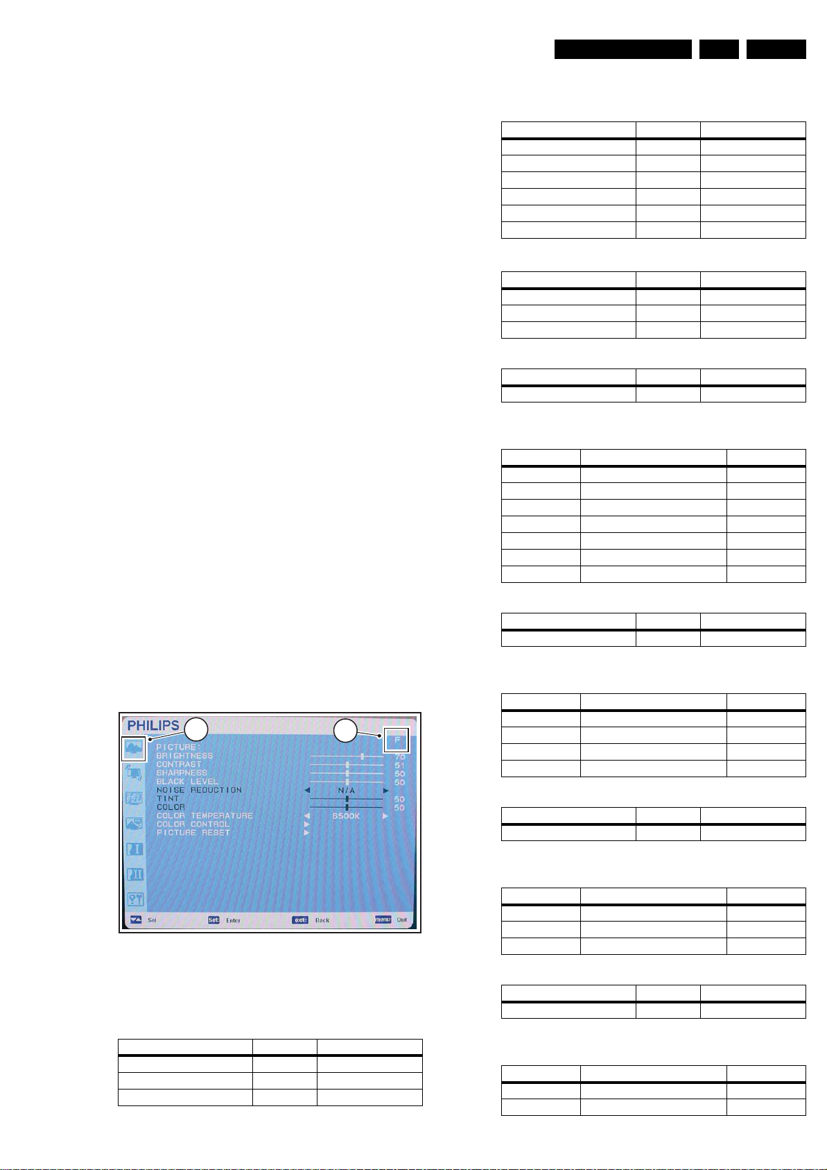
8. Alignments
Alignments
EN 43QCS1.0S LA 8.
Index of this chapter:
8.1 General Alignment Conditions
8.2 Hardware Alignments
8.3 Software Alignments
8.4 Option Settings
8.5 Software update
8.1 General Alignment Conditions
Perform all electrical adjustments under the following
conditions:
• Power supply voltage (depends on region):
– AP-NTSC: 120 V
– AP-PAL-multi: 120 - 230 V
– EU: 230 V
– LATAM-NTSC: 120 - 230 V
– US: 120 V
• Connect the set to the mains via an isolation transformer
with low internal resistance.
• Allow the set to warm up for approximately 25 minutes.
• Measure voltages and waveforms in relation to correct
ground (e.g. measure audio signals in relation to
AUDIO_GND).
Caution: It is not allowed to use heatsinks as ground.
• Test probe: Ri > 10 Mohm, Ci < 20 pF.
• Use an isolated trimmer/screwdriver to perform
alignments.
AC
AC
or 230 VAC / 50 Hz (± 10%).
AC
/ 50 Hz (± 10%).
/ 60 Hz (± 10%).
/ 50 Hz (± 10%).
AC
/ 50 Hz (± 10%).
AC
8.2 Hardware Alignments
This chassis does not contain any hardware alignments.
Setting Range Default value
Black level 0 to 100 50
Noise reduction - OFF
Tint 0 to 100 50
Color 0 to 100 50
Color temperature 9300 K
Picture reset Submenu -
Color control
Setting Range Default value
User R 0 to 255 255
User G 0 to 255 255
User B 0 to 255 255
Picture reset
Setting Range Default value
Picture reset Yes/No No
8.3.2 Screen defaults
Setting Range Default value
H position 0 to 100 50
V position 0 to 100 50
Clock 0 to 100 50
Clock phase 0 to 100 50
Zoom mode Full, Real, Custom, Normal Real
Custom zoom custom Screen reset Submenu -
8.3 Software Alignments
Refer to figure “Factory Mode Indication” for details.
Put the set in the Factory mode see Chapter “Service Modes,
Error Codes, and Fault Finding”, section “Service Mode”. The
“F” [2] in the Picture menu [1] indicates the set is in factory
mode. Use the navigation keys to browse through the menu.
1
Figure 8-1 Factory Mode Indication
8.3.1 Picture defaults
2
I_17540_015.eps
310108
Screen reset
Setting Range Default value
Screen reset Yes/No No
8.3.3 Audio defaults
Setting Range Default value
Balance 0 to 100 50
Treble 0 to 100 50
Bass 0 to 100 50
Audio reset Submenu -
Audio reset
Setting Range Default value
Audio reset Yes/No No
8.3.4 PIP defaults
Setting Range Default value
PIP size Small, Middle, Large Small
PIP audio Main, Sub Main
PIP reset Submenu -
PIP reset
Setting Range Default value
PIP reset Yes/No No
Setting Range Default value
Brightness 0 to 100 50
Contrast 0 to 100 50
Sharpness 0 to 100 50
8.3.5 Configuration 1 defaults
Setting Range Default value
Auto adjust Submenu Power save Submenu -
Page 44
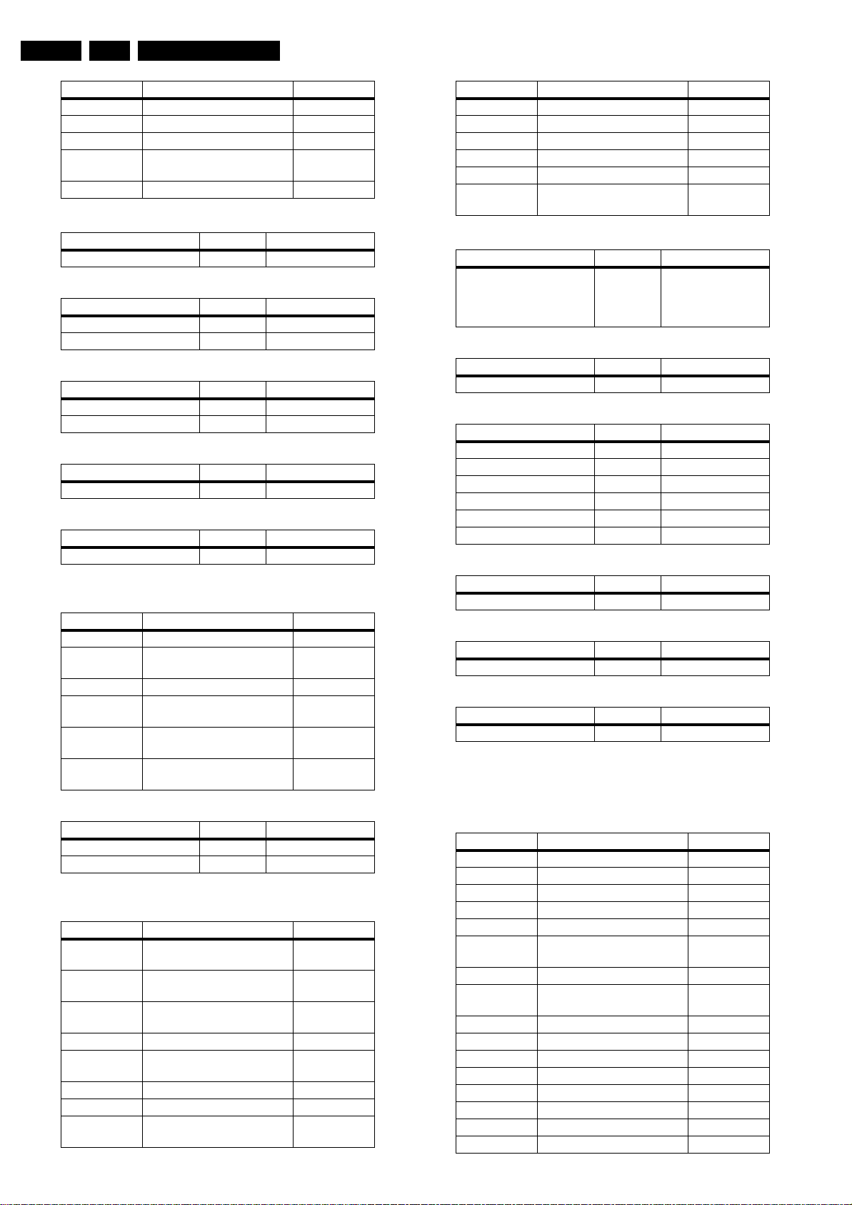
EN 44 QCS1.0S LA8.
Alignments
Setting Range Default value
Language - English
Panel saving Submenu Color system - N/A
Configuration
reset
Factory reset Submenu -
Auto adjust
Setting Range Default value
Auto adjust - N/A
Power save
Setting Range Default value
RGB On/Off Off
Video On/Off Off
Panel saving
Setting Range Default value
Brightness On/Off Off
Pixel Shift On/Off Off
Configuration reset
Setting Range Default value
Configuration reset Yes/No No
Factory reset
Setting Range Default value
Factory reset Yes/No No
8.3.6 Configuration 2 defaults
Setting Range Default value
OSD turn off 0 to 100 50
Information
OSD
Sleep timer 1 to 24 hrs. or off Off
OSD H
position
OSD V
position
Monitor
information
Monitor information
Setting Range Default value
Model name - Type number
Serial no Serial number
8.3.7 Advanced option defaults
Setting Range Default value
Input
resolution
Black level
expansion
Gamma
selection
Scan mode - Overscan
Scan
conversion
Film mode - Auto
IR control Submenu Keyboard
control
Submenu -
1 to 10 sec 10 sec
0 to 100 50
0 to 100 50
Submenu -
-N/A
On/off Off
Native, 2.4, 2.4, S gamma Native
- Progressive
Submenu -
Setting Range Default value
Tiling Submenu Date and time Submenu Schedule Submenu Monitor ID Submenu DDC/CI On/off On
Advanced
option reset
IR control
Setting Range Default value
IR control Normal,
Keyboard control
Setting Range Default value
Keyboard control Yes/No No
Date and time
Setting Range Default value
Year - Month - Day - Hour - Minute - Daylight saving time On/off Off
Schedule
Setting Range Default value
Schedule setting by user - -
Monitor ID
Setting Range Default value
Monitor ID - 1
Advanced option reset
Setting Range Default value
Advanced option reset Yes/No No
8.3.8 Factory Setting defaults
Remark: The entry for the factory setting is not visible, but is
located below the Advanced option menu. This menu is only
available when the set is in factory mode.
Setting Range Default value
Burn in On/off (see note 1) Off
Hours running Submenu Factory reset Submenu ADC adjust Submenu Brightness Submenu Color
temperature
SMT 0, 1 0
EDID write
protect
OSD off On/off Off
Frame lock On/off On
Self diag Submenu N/A
A setting Submenu N/A
VT mode Submenu DDR control Submenu N/A
ID edit Submenu N/A
EEP edit On/off On
Submenu -
Normal
Lock,
Primary,
Secondary
Submenu -
On/off On
Page 45
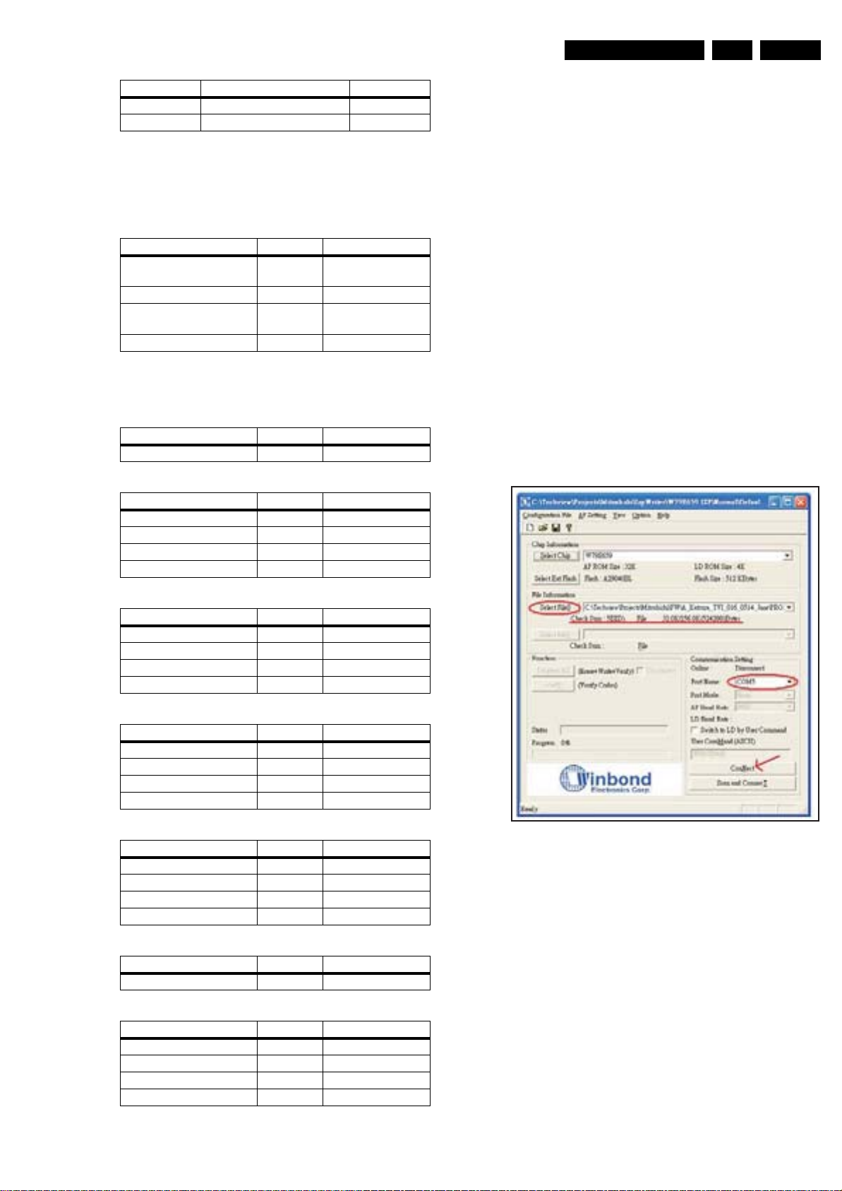
Alignments
EN 45QCS1.0S LA 8.
Setting Range Default value
Version Submenu SSC Submenu N/A
Note:
1. This function turns enables a monitor to burn in without an
input signal by showing the following burn in pattern cycle:
white, black, red, green, blue.
Hours running
Setting Resetable Default value
Resetable on Yes Monitor power on
time
Resetable off Yes Power save time
Unresetable on No monitor power on
time
Unresetable off No Power save time
Note: Power save time is the total time of stand by mode,
suspend mode and off mode.
Factory reset
Setting Range Default value
Factory reset Yes/No No
ADC adjust
Setting Range Default value
D sub ADC adjust Submenu BNC ADC adjust Submenu YPbPr ADC adjust Submenu Video ADC adjust Submenu -
8.4 Option Settings
Not applicable.
8.5 Software update
8.5.1 Hardware
Connect the cable of RS232 with PC COM port by jump wire.
8.5.2 Firmware
Open the 8051IspWriter.exe. Note the following:
1. Select File0: select the correct BIOS.
2. Com Port: Select the correct Port Number.
3. Click the “ConNect”. It is normal that the picture
disappears. The BIOS is writing now. Please wait a
moment.
4. Click the “ConNect” button. It shows an error message
when it cannot connect. Recheck if the “Auto program” is
selected and Auto connect didn't select within “Option”.
Double check the port number.
5. Turn “off” the power if this fails. Remain pushing the reset
button of Winbond Micron. Then turn on the power and
restart from step 3. Release the reset button when BIOS is
writing normal.
Brightness
Setting Range Default value
PC max brightness 0 to 255 255
PC min brightness 0 to 255 0
Video max brightness 0 to 255 255
Video min brightness 0 to 255 0
Color temperature
Setting Range Default value
Color temperature - 9300K
User R 0 to 255 255
User G 0 to 255 255
User B 0 to 255 255
VT mode
Setting Range Default value
White - 0
Red - 0
Green - 0
Blue - 0
Version
Setting Range Default value
Version ID - -
Figure 8-2 Factory Mode Indication
I_17540_048.eps
310108
SSC
Setting Range Default value
SSC on/off On/off On
SSC scan (kHz) - 80
SSC step (/100) - 1
SSC DDR On/off On
Page 46

EN 46 QCS1.0S LA9.
Circuit Descriptions, Abbreviation List, and IC Data Sheets
9. Circuit Descriptions, Abbreviation List, and IC Data Sheets
Index of this chapter:
9.1 Mstar MST5251A scaler
9.2 NEC uPD64015 Video Decoder
9.3 TI PCM1753 Audio DAC
9.4 JRC NJW1141 Audio Processor
9.5 Winbond W79E659 MCU
9.6 Fintek F75101R GPIO Expander
9.7 Eon EN29F040A 4MBit Flash
9.8 YAMAHA YDA138 Audio Amplifier
9.9 Sipex SP3243 RS-232 transceiver
9.10 Mitsumi MM1671 Low Supply Voltage 75 W Driver
9.11 EtronTech EM636165TS-5G SDRAM
9.12 National Semiconductor LM1881 Video Sync Separator
9.13 NXP PCF8563 RTC
9.14 ST TSH340 Video Buffer
9.15 Pericom PI5C3253 Dual 1-of-4 FET Multiplexer/
Demultiplexer
9.16 ATMEL AT24C64AN EPROM
9.17 Abbreviation List
9.1 Mstar MST5251A scaler
The MST5251A is a high performance and fully integrated
graphics processing IC solution for multi-function LCD monitor/
TV with resolutions up to UXGA/WUXGA. It is configured with
an integrated triple-ADC/PLL, an integrated DVI/HDCP/HDMI
receiver, two video de-interlacers, two high quality scaling
engines, an on-screen display controller, and a built-in output
clock generator. By use of external frame buffer, PIP/POP is
provided for multimedia applications. It supports de-interlaced
full-screen video, video-on-graphic overlay, split screen, frame
rate conversion, and aspect ratio conversion for various video
sources. To further reduce system costs, the MST5251A also
integrates intelligent power management, control capability for
green-mode requirements and spreadspectrum support for
EMI management.
9.2 NEC uPD64015 Video Decoder
9.4 JRC NJW1141 Audio Processor
The NJW1141 is a sound processor includes all of the
functions required to process the audio signal for TV, such as
tone control, balance, volume, mute, and AGC functions. All of
the internal status and variables are controlled by I
interface.
9.5 Winbond W79E659 MCU
The W79E659 is a fast, 8051/52-compatible microcontroller
with a redesigned processor core that eliminates wasted clock
and memory cycles. Typically, the W79E659 executes
instructions 1.5 to 3 times faster than that of the traditional
8051/52, depending on the type of instruction, and the overall
performance is about 2.5 times better at the same crystal
speed. As a result, with the fully-static CMOS design, the
W79E659 can accomplish the same throughput with a lower
clock speed, reducing power consumption. The W79E659
provides 256 bytes of on-chip RAM; 1-KB of auxiliary RAM;
seven 8-bit, bi-directional and bit-addressable I/O ports; an
additional 4-bit port P4; three 16-bit timer/counters; an UART
serial port, 2 channels of I
8 channels of 10-bit ADC. These peripherals are all supported
by ten interrupt sources with 2 levels of priority. The W79E659
contains a 32-KB Flash EPROM whose contents may be
updated in-system by a loader program stored in an auxiliary,
4-KB Flash EPROM. Once the contents are confirmed, it can
be protected for security.
2
C with master/slave capability and
9.6 Fintek F75101R GPIO Expander
The F75101R is a multi functional general purpose I/O chip
providing 16 GPIO powered by 3VSB by power on setting.
Level or pulse modes can be programmed by registers. With
2 sets of watchdog timer, F75101R provides more flexible
control for system.
2
C bus
The uPD64015 is a video decoder LSI with an on-chip
threedimensional Y/C separation function that supports
NTSC-M and PAL-BDGHI composite signals and a
threedimensional noise reduction function that supports all
input signals. It includes four high-accuracy A/D converter
channels for analog video input, an anti-alias filter, Y/C
separation, chroma decoding supporting NTSC/PAL/SECAM,
threedimensional noise reduction supporting all input signals,
and various definition correction functions, and supports digital
colour difference output. The uPD64015 incorporates a 3channel DAC and can output decoded video signals or signals
output from the incorporated SG (Signal Generator), in the form
of RGB or analog colour difference signals.
9.3 TI PCM1753 Audio DAC
The PCM1753/54/55 is a CMOS, monolithic, integrated circuit,
which includes stereo digital-to-analog converters and support
circuitry in a small 16-lead SSOP package. The data
converters use TI's enhanced multi level delta-sigma
architecture, which employs 4
amplitude quantization to achieve excellent dynamic
performance and improved tolerance to clock jitter. The
PCM1753/54/55 accepts industry standard audio data formats
with 16- to 24-bit data, providing easy interfacing to audio DSP
and decoder chips. Sampling rates up to 200 kHz are
supported. A full set of user programmable functions is
accessible through a three wire serial control port, which
supports register write functions.
th
order noise shaping and 8-level
9.7 Eon EN29F040A 4MBit Flash
The EN29F040A is a 4-Megabit, electrically erasable, read/
write non-volatile flash memory organized into 512K words with
8 bits per word, the 4M of memory is arranged in eight uniform
sectors of 64 Kilobytes each. Any byte can be programmed
typically in 10 μs. The EN29F040A features 5.0 V voltage read
and write operation, with access times as fast as 45 ns to
eliminate the need for WAIT states in high-performance
microprocessor systems.
9.8 YAMAHA YDA138 Audio Amplifier
The YDA138 (D-3) is a high efficient digital audio power
amplifier IC that operates with a single 12 V power supply. An
audio power amplifier with a maximum output of 10 W (R
8 Ω) 2 channels can be configured with one chip. YDA138 has
a “Pure Pulse Direct Speaker Drive Circuit” which directly
drives speakers while reducing distortion of pulse output signal
and reducing noise on the signal, and realizes the highest
standard low distortion rate characteristics and low noise
characteristics as 10 W-class of output digital amplifier IC. In
addition, circuit design with fewer external parts can be made
depend on the condition of use because corresponds to filter
less. YDA138 provides overcurrent protection function for
speaker output terminals, IC thermal protection function, POP
noise reduction function, and AM interference measures
function as well as power-down and output mute functions.
=
L
Page 47

Circuit Descriptions, Abbreviation List, and IC Data Sheets
EN 47QCS1.0S LA 9.
9.9 Sipex SP3243 RS-232 transceiver
The SP3243 transceivers meet the EIA/TIA-232 and ITU-T
V.28/V.24 communication protocols. Generates 5.5V RS-232
voltage levels from a single +3.0V to +5.5V power supply and
operates at a data rate of 120 kbps fully loaded. The SP3243
devices feature AUTO ON-LINE® circuitry automatically wakes
up from a 1 μA shutdown. It occurs after a RS-232 cable being
disconnected. Under this condition, the internal charge pump
and the drivers will be shut down. Otherwise, the system
automatically comes on-line.
9.10 Mitsumi MM1671 Low Supply Voltage 75 Ω
Driver
This IC is a 75Ù driver with a built-in LPF that can operate at
low voltage. It supports 3 V and 5 V operating power voltage,
and is ideal for video signal output in devices ranging from
portable digital still cameras to stationary equipment such as
DVD players. It incorporates a high performance 4-stage LPF,
which is ideal for removing DAC sampling noise. In addition,
ultra-low current consumption has been achieved by
suppressing current consumption during power save to
under1 μA. This lengthens the life of the batteries in portable
devices. The built-in amp gain on this IC is available in series:
6 dB/9 dB/12 dB/16.5 dB, thus enabling support for DAC and a
variety of output amplitudes. There is also a series with input
clamp and one without, allowing support for a range of video
signals, not just composite signals.
9.13 NXP PCF8563 RTC
The PCF8563 is a CMOS real-time clock/calendar optimized
for low power consumption. A programmable clock output,
interrupt output and voltage-low detector are also provided. All
address and data are transferred serially via a two-line
bidirectional I
built-in word address register is incremented automatically
after each written or read data byte.
2
C-bus. Maximum bus speed is 400 kbits/s. The
9.14 ST TSH340 Video Buffer
The TSH340 is a video buffer featuring a gain of 6 dB. A large
bandwidth of 300 MHz for only 9.4 mA of quiescent current
allows the TSH340 to achieve a gain flatness of 220 MHz. Its
structure features a very high slew rate of 540 V/μs minimum
guaranteed by test. Associated to a very good THD these
characteristics are particularly intended in the high quality
video systems. The TSH340 is available in tiny SOT23-5 and
SO8 plastic packages for size saving consideration.
9.15 Pericom PI5C3253 Dual 1-of-4 FET Multiplexer/ Demultiplexer
Pericom Semiconductor's PI5C3253 is a Dual 4 : 1 Multiplexer/
demultiplexer with three-state outputs that is pinout compatible
with the PI74FCT253T, 74F253, and 74ALS/AS/LS 253. Inputs
can be connected to outputs with low on resistance (5 Ω) with
no additional ground bounce noise or propagation delay.
9.11 EtronTech EM636165TS-5G SDRAM
The EM636165 SDRAM is a high-speed CMOS synchronous
DRAM containing 16 Mbits. It is internally configured as a dual
512K word × 16 DRAM with a synchronous interface (all signals
are registered on the positive edge of the clock signal, CLK).
Each of the 512K × 16 bit banks is organized as 2048 rows by
256 columns by 16 bits. Read and write accesses to the
SDRAM are burst oriented; accesses start at a selected
location and continue for a programmed number of locations in
a programmed sequence. Accesses begin with the registration
of a BankActivate command which is then followed by a Read
or Write command. The EM636165 provides for programmable
Read or Write burst lengths of 1, 2, 4, 8, or full page, with a
burst termination option. An auto precharge function may be
enabled to provide a self-timed row precharge that is initiated
at the end of the burst sequence. The refresh functions, either
Auto or Self Refresh are easy to use. By having a
programmable mode register, the system can choose the most
suitable modes to maximize its performance. These devices
are well suited for applications requiring high memory
bandwidth and particularly well suited to high performance PC
applications.
9.12 National Semiconductor LM1881 Video Sync Separator
The LM1881 Video sync separator extracts timing information
including composite and vertical sync, burst/back porch timing,
and odd/even field information from standard negative going
sync NTSC, PAL*, and SECAM video signals with amplitude
from 0.5 V to 2 V
providing sync separation for non-standard, faster horizontal
rate video signals. The vertical output is produced on the rising
edge of the first serration in the vertical sync period. A default
vertical output is produced after a time delay if the rising edge
mentioned above does not occur within the externally set delay
period, such as might be the case for a non-standard video
signal.
. The integrated circuit is also capable of
p-p
9.16 ATMEL AT24C64AN EPROM
The AT24C32A/64A provides 32,768/65,536 bits of serial
electrically erasable and programmable read only memory
(EEPROM) organized as 4096/8192 words of 8 bits each. The
device's cascadable feature allows up to 8 devices to share a
common twowire bus. The device is optimized for use in many
industrial and commercial applications where low power and
low voltage operation are essential. The AT24C32A/64A is
available in space saving 8-lead JEDEC PDIP, 8-lead JEDEC
SOIC, 8-lead EIAJ SOIC, 8-lead Mini-MAP (MLP 2x3) and 8lead TSSOP packages and is accessed via a 2-wire serial
interface. In addition, the entire family is available in 2.7 V
(2.7 V to 5.5 V) and 1.8 V (1.8 V to 5.5 V) versions.
Page 48

EN 48 QCS1.0S LA9.
Circuit Descriptions, Abbreviation List, and IC Data Sheets
9.17 Abbreviation List
1080i. 1080 visible lines, interlaced
1080p. 1080 visible lines, progressive scan
2CS. 2 Carrier Sound
2DNR. Spatial (2D) Noise Reduction
3DNR. Temporal (3D) Noise Reduction
480i. 480 visible lines, interlaced
480p. 480 visible lines, progressive scan
AARA. Automatic Aspect Ratio Adaptation:
algorithm that adapts aspect ratio to
remove horizontal black bars; keeping
up the original aspect ratio
ACI. Automatic Channel Installation:
algorithm that installs TV channels
directly from a cable network by
means of a predefined TXT page
ADC. Analogue to Digital Converter
AFC. Automatic Frequency Control: control
signal used to tune to the correct
frequency
AGC. Automatic Gain Control: algorithm that
controls the video input of the feature
box
AM. Amplitude Modulation
AUO. Acer Unipack Optronics
AP. Asia Pacific
AR. Aspect Ratio: 4 by 3 or 16 by 9
ASD. Automatic Standard Detection
AV. Audio Video
B-SC1-IN. Blue SCART1 in
B-SC2-IN. Blue SCART2 in
B-TXT. Blue teletext
B/G. Monochrome TV system. Sound
carrier distance is 5.5 MHz
BTSC. Broadcast Television System
Committee
C-FRONT. Chrominance front input
CBA. Circuit Board Assembly (or PWB)
CL. Constant Level: audio output to
connect with an external amplifier
CLUT. Colour Look Up Table
ComPair. Computer aided rePair
CSM. Customer Service Mode
CVBS. Composite Video Blanking and
Synchronisation
CVBS-EXT. CVBS signal from external source
(VCR, VCD, etc.)
CVBS-INT. CVBS signal from Tuner
CVBS-MON. CVBS monitor signal
CVBS-TER-OUT. CVBS terrestrial out
DAC. Digital to Analogue Converter
DBE. Dynamic Bass Enhancement: extra
low frequency amplification
DFU. Directions For Use: owner's manual
DNR. Dynamic Noise Reduction
DRAM. Dynamic RAM
DSP. Digital Signal Processing
DST. Dealer Service Tool: special
(European) remote control designed
for service technicians
DTS. Digital Theatre Sound
DVD. Digital Versatile Disc
DVI. Digital Visual Interface
DW. Double Window
ED. Enhanced Definition: 480p, 576p
EEPROM. Electrically Erasable and
Programmable Read Only Memory
EU. EUrope
EXT. EXTernal (source), entering the set by
SCART or by cinches (jacks)
FBL. Fast Blanking: DC signal
accompanying RGB signals
FBL-SC1-IN. Fast blanking signal for SCART1 in
FBL-SC2-IN. Fast blanking signal for SCART2 in
FBL-TXT. Fast Blanking Teletext
FLASH. FLASH memory
FM. Field Memory / Frequency Modulation
FMR. FM Radio
FRC. Frame Rate Converter
FRONT-C. Front input chrominance (SVHS)
FRONT-DETECT. Front input detection
FRONT-Y_CVBS. Front input luminance or CVBS
(SVHS)
FTV. Flat TeleVision
G-SC1-IN. Green SCART1 in
G-SC2-IN. Green SCART2 in
G-TXT. Green teletext
H. H_sync to the module
HD. High Definition: 720p, 1080i, 1080p
HDMI. High Definition Multimedia Interface,
digital audio and video interface
HP. Head Phone
I. Monochrome TV system. Sound
carrier distance is 6.0 MHz
I2C. Integrated IC bus
I2S. Integrated IC Sound bus
IC. Integrated Circuit
IF. Intermediate Frequency
Interlaced. Scan mode where two fields are used
to form one frame. Each field contains
half the number of the total amount of
lines. The fields are written in "pairs",
causing line flicker.
IR. Infra Red
IRQ. Interrupt ReQuest
Last Status. The settings last chosen by the
customer and read and stored in RAM
or in the NVM. They are called at start-
up of the set to configure it according
the customers wishes
LATAM. LATin AMerica
LC04. Philips chassis name for LCD TV 2004
project
LCD. Liquid Crystal Display
LED. Light Emitting Diode
L/L'. Monochrome TV system. Sound
carrier distance is 6.5 MHz. L' is Band
I, L is all bands except for Band I
LPL. LG Philips LCD
LS. Loud Speaker
LVDS. Low Voltage Differential Signalling,
data transmission system for high
speed and low EMI communication.
M/N. Monochrome TV system. Sound
carrier distance is 4.5 MHz
MOSFET. Metal Oxide Semiconductor Field
Effect Transistor
MPEG. Motion Pictures Experts Group
MSP. Multi-standard Sound Processor: ITT
sound decoder
MUTE. MUTE Line
NAFTA. North American Free Trade
Association: Trade agreement
between Canada, USA and Mexico
NC. Not Connected
NICAM. Near Instantaneous Compounded
Audio Multiplexing. This is a digital
sound system, used mainly in Europe.
NTSC. National Television Standard
Committee. Colour system used
mainly in North America and Japan.
Colour carrier NTSC M/N = 3.579545
MHz, NTSC 4.43 = 4.433619 MHz
(this is a VCR norm, it is not
transmitted off-air)
NVM. Non Volatile Memory: IC containing
TV related data (for example, options)
O/C. Open Circuit
Page 49

Circuit Descriptions, Abbreviation List, and IC Data Sheets
EN 49QCS1.0S LA 9.
ON/OFF LED. On/Off control signal for the LED
OSD. On Screen Display
PAL. Phase Alternating Line. Colour system
used mainly in Western Europe
(colour carrier = 4.433619 MHz) and
South America (colour carrier PAL M =
3.575612 MHz and PAL N = 3.582056
MHz)
PC. Personal Computer
PCB. Printed Circuit Board (or PWB)
PDP. Plasma Display Panel
PIG. Picture In Graphic
PIP. Picture In Picture
PLL. Phase Locked Loop. Used, for
example, in FST tuning systems. The
customer can directly provide the
desired frequency
Progressive Scan. Scan mode where all scan lines are
displayed in one frame at the same
time, creating a double vertical
resolution.
PWB. Printed Wiring Board (or PCB)
RAM. Random Access Memory
RC. Remote Control transmitter
RC5 (6). Remote Control system 5 (6), the
signal from the remote control receiver
RGB. Red, Green, and Blue. The primary
colour signals for TV. By mixing levels
of R, G, and B, all colours (Y/C) are
reproduced.
RGBHV. Red, Green, Blue, Horizontal sync,
and Vertical sync
ROM. Read Only Memory
SAM. Service Alignment Mode
SC. SandCastle: two-level pulse derived
from sync signals
SC1-OUT. SCART output of the MSP audio IC
SC2-B-IN. SCART2 Blue in
SC2-C-IN. SCART2 chrominance in
SC2-OUT. SCART output of the MSP audio IC
S/C. Short Circuit
SCL. Clock signal on I2C bus
SD. Standard Definition: 480i, 576i
SDA. Data signal on I2C bus
SDI. Samsung Display Industry
SDM. Service Default Mode
SDRAM. Synchronous DRAM
SECAM. SEequence Couleur Avec Memoire.
Colour system used mainly in France
and Eastern Europe. Colour carriers =
4.406250 MHz and 4.250000 MHz
SIF. Sound Intermediate Frequency
SMPS. Switch Mode Power Supply
SND. SouND
SNDL-SC1-IN. Sound left SCART1 in
SNDL-SC1-OUT. Sound left SCART1 out
SNDL-SC2-IN. Sound left SCART2 in
SNDL-SC2-OUT. Sound left SCART2 out
SNDR-SC1-IN. Sound right SCART1 in
SNDR-SC1-OUT. Sound right SCART1 out
SNDR-SC2-IN. Sound right SCART2 out
SNDR-SC2-OUT. Sound right SCART2 out
SNDS-VL-OUT. Surround sound left variable level out
SNDS-VR-OUT. Surround sound right variable level out
SOPS. Self Oscillating Power Supply
S/PDIF. Sony Philips Digital InterFace
SRAM. Static RAM
STBY. Stand-by
SVHS. Super Video Home System
SW. Sub Woofer / SoftWare
THD. Total Harmonic Distortion
TXT. TeleteXT
uP. Microprocessor
VL. Variable Level out: processed audio
output toward external amplifier
VCR. Video Cassette Recorder
VGA. Video Graphics Array
WD. Watch Dog
WYSIWYR. What You See Is What You Record:
record selection that follows main
picture and sound
XTAL. Quartz crystal
YPbPr. Component video (Y= Luminance, Pb/
Pr= Colour difference signals B-Y and
R-Y, other amplitudes w.r.t. to YUV)
Y/C. Video related signals: Y consists of
luminance signal, blanking level and
sync; C consists of colour signal.
Y-OUT. Luminance-signal
YUV. Baseband component video (Y=
Luminance, U/V= Colour difference
signals)
Page 50
EN 50 QCS1.0S LA10.
10. Spare Parts List
Set Level
BDL4631V/00
0001 9965 100 10746 Front bezel assembly
0003 9965 100 10747 Back cover assembly
0012 9965 100 10736 46" LK46D3LZ1 1080P
0020 9965 100 10749 Main Board [S-A]
0021 9965 100 10748 Power Board [P]
0022 9965 100 10750 Speaker Board [SP]
0025 9965 100 10752 Button Board [B]
0040 9965 100 10751 LED Board [L]
0050 9965 100 10753 Remote control
0100 9965 100 10737 MB-LCD cable
0110 9965 100 10738 Speaker/B-MB cable
0130 9965 100 10740 Power-AC Switch
0150 9965 100 10742 Power-MB cable
0160 9965 100 10743 PWR-INV/B cable
0180 9965 100 10745 MB-Key/B
Spare Parts List
Page 51

11. Revision List
Manual xxxx xxx xxxx.0
• First release.
Revision List
EN 51QCS1.0S LA 11.
 Loading...