

Philips BCV63B Datasheet
DISCRETE SEMICONDUCTORS
DATA SH EET
M3D071
BCV63; BCV63B
NPN general purpose double
transistors
Product specification
Supersedes data of 1997 Mar 10
1999 May 21

Philips Semiconductors Product specification
NPN general purpose double transistors BCV63; BCV63B
FEA TURES
• Low current (max. 100 mA)
PINNING
PIN DESCRIPTION
• Low voltage (max. 30 and 6 V).
APPLICATIONS
• General purpose switching and amplification
• For use in Schmitt-trigger applications.
DESCRIPTION
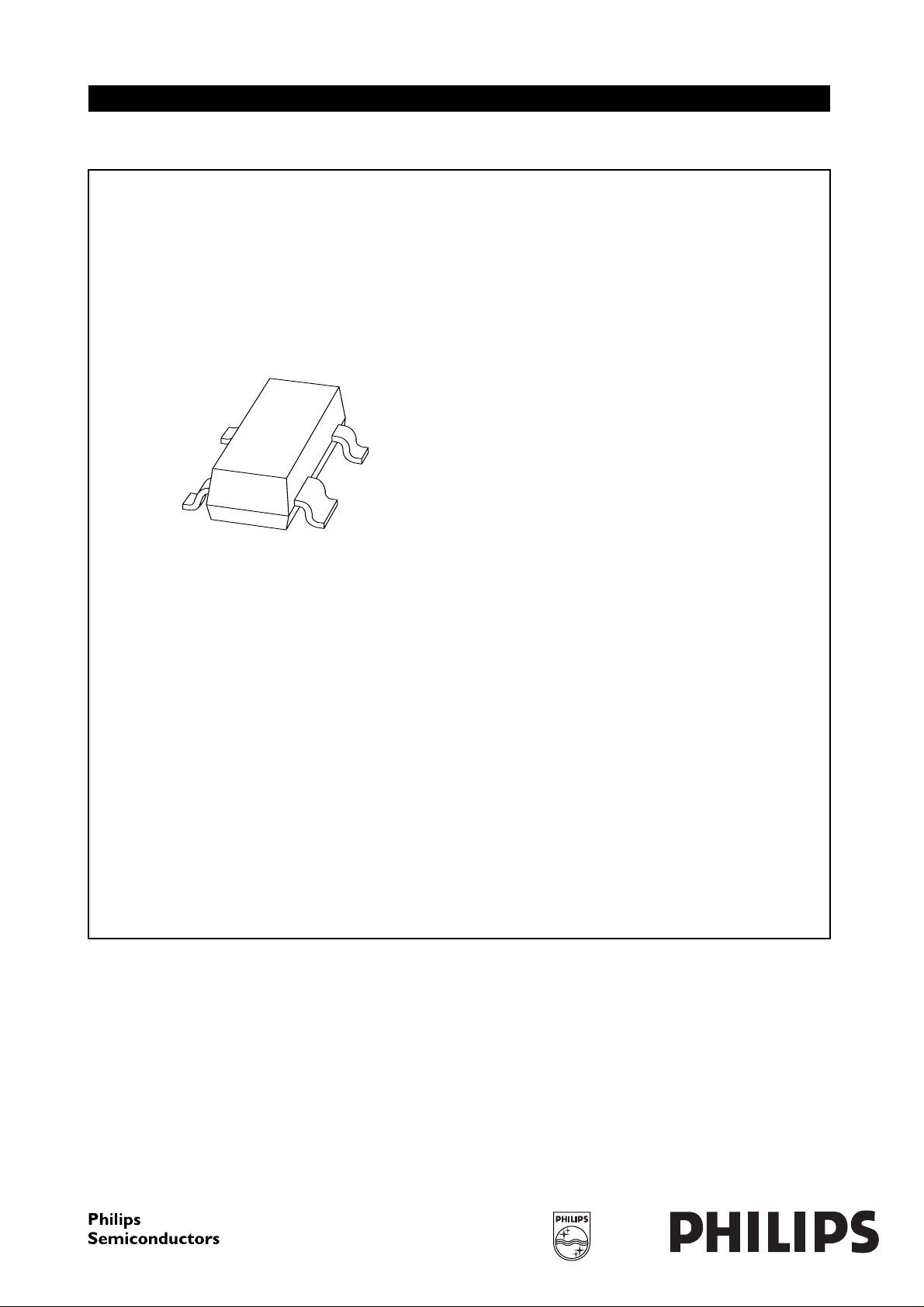
handbook, halfpage
NPN double transistor in a SOT143B plastic package.
PNP complement: BCV64B.
MARKING
TYPE NUMBER MARKING CODE
BCV63 D95
Fig.1 Simplified outline (SOT143B) and symbol.
BCV63B D96
LIMITING VALUES
In accordance with the Absolute Maximum Rating System (IEC 134).
1 collector TR2 and base TR1
2 collector TR1
3 emitter TR1 and TR2
4 base TR2
21
TR1
TR2
34
Top view
4
3
12
MAM316
SYMBOL PARAMETER CONDITIONS MIN. MAX. UNIT
V
CBO
collector-base voltage open emitter
TR1 − 30 V
TR2 − 6V
V
CEO
collector-emitter voltage open base
TR1 − 30 V
TR2 − 6V
V
EBO
I
C
I
CM
I
B
P
tot
T
stg
T
j
T
amb
emitter-base voltage open collector − 6V
collector current (DC) − 100 mA
peak collector current − 200 mA
base current (DC) − 100 mA
total power dissipation T
≤ 25 °C; note 1 − 250 mW
amb
storage temperature −65 +150 °C
junction temperature − 150 °C
operating ambient temperature −65 +150 °C
Note
1. Transistor mounted on a printed-circuit board.
1999 May 21 2

Philips Semiconductors Product specification
NPN general purpose double transistors BCV63; BCV63B
THERMAL CHARACTERISTICS
SYMBOL PARAMETER CONDITIONS VALUE UNIT
R
th j-a
Note
1. Transistor mounted on a printed-circuit board.
CHARACTERISTICS
=25°C unless otherwise specified.
T
amb
SYMBOL PARAMETER CONDITIONS MIN. TYP. MAX. UNIT
I
CBO
h
FE
V
CEsat
V
BEsat
V
BE
C
c
f
T
thermal resistance from junction to ambient note 1 500 K/W
collector cut-off current IE= 0; VCB=30V −−15 nA
I
= 0; VCB= 30 V; Tj= 150 °C −−5µA
E
DC current gain
BCV63 TR1 I
BCV63 TR2 I
BCV63B TR1 I
BCV63B TR2 I
= 2 mA; VCE=5V 110 − 800
C
= 2 mA; VCE= 700 mV; note 1 110 − 800
C
= 2 mA; VCE= 5 V 200 − 450
C
= 2 mA; VCE= 700 mV; note 1 200 − 450
C
collector-emitter saturation voltage IC= 10 mA; IB= 0.5 mA − 75 300 mV
collector-emitter saturation voltage I
= 100 mA; IB=5mA
C
TR1 − 250 650 mV
TR2 − 250 − mV
base-emitter saturation voltage IC= 10 mA; IB= 0.5 mA; note 2 − 700 − mV
base-emitter saturation voltage I
= 100 mA; IB= 5 mA; note 2
C
TR1 −−850 − mV
base-emitter voltage
TR1 I
TR1 I
TR2 I
= 2 mA; VCE= 5 V; note 3 600 650 750 mV
C
= 10 mA; VCE= 5 V; note 3 −−820 mV
C
= 2 mA; VCE= 700 mV; note 3 − 700 − mV
C
collector capacitance IE=ie= 0; VCB= 10 V; f = 1 MHz
TR1 − 4 − pF
transition frequency IC= 10 mA; VCE= 5 V; f = 100 MHz
TR1 100 −−MHz
Notes
1. Group selection will be done on TR1. Due to matched dies, h
2. V
decreases by approximately 1.7 mV/K with increasing temperature.
BEsat
values for TR2 are the same as for TR1.
FE
3. VBE decreases by approximately 2 mV/K with increasing temperature.
1999 May 21 3
 Loading...