

Philips BCV62C, BCV62B, BCV62A, BCV62 Datasheet
DISCRETE SEMICONDUCTORS
DATA SH EET
M3D071
BCV62
PNP general purpose
double transistor
Product specification
Supersedes data of 1997 Jun 18
1999 Apr 08
Philips Semiconductors Product specification
PNP general purpose double transistor BCV62
FEATURES
• Low current (max. 100 mA)
• Low voltage (max. 30 V)
• Matched pair.
APPLICATIONS
• For use in applications where the working point must be
independent of temperature
• Current mirrors.
DESCRIPTION
PNP double transistor in a SOT143B plastic package.
NPN complement: BCV61.
MARKING
TYPE
NUMBER
MARKING
CODE
TYPE
NUMBER
MARKING
CODE
BCV62 3Mp BCV62B 3Kp
BCV62A 3Jp BCV62C 3Lp
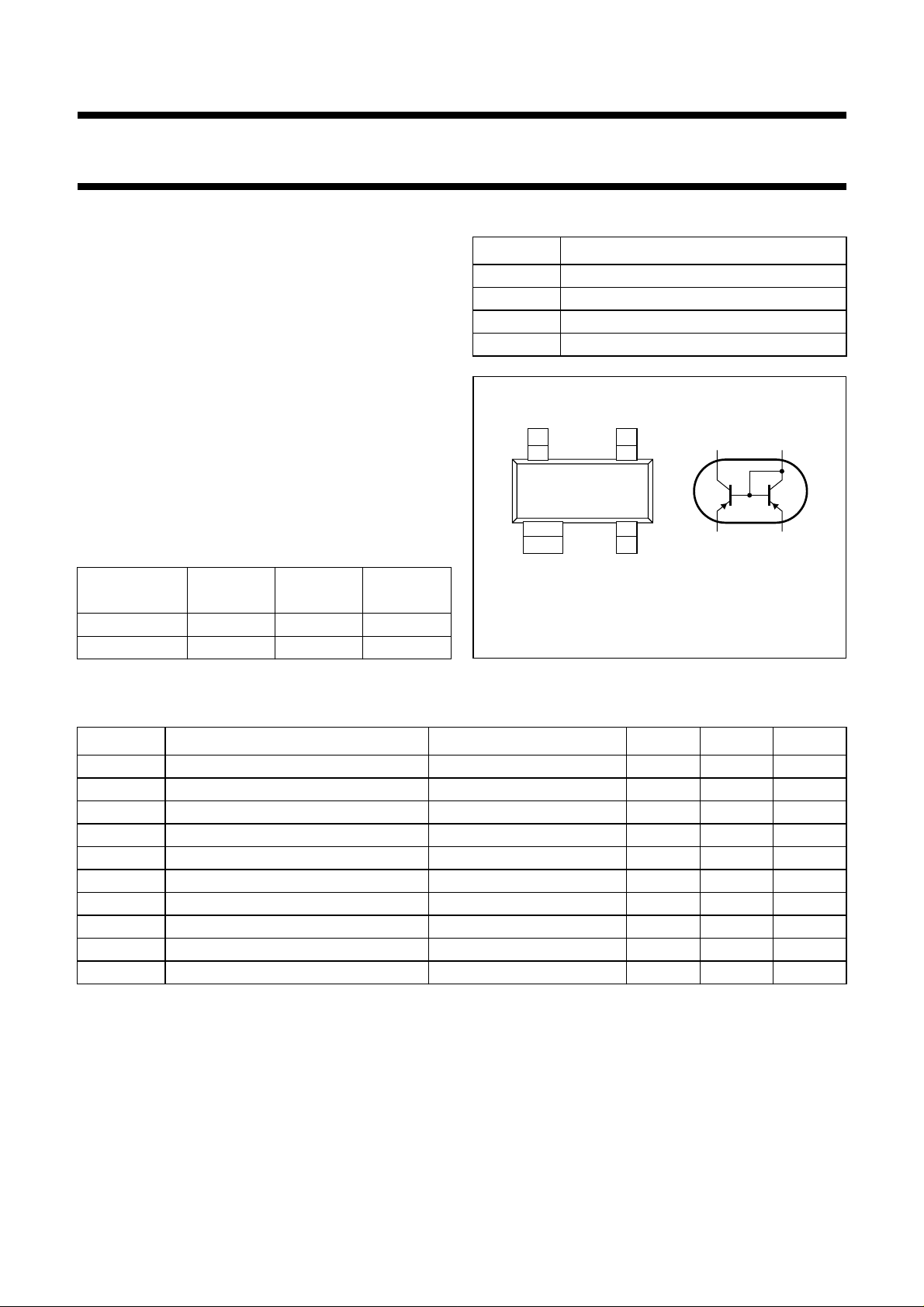
PINNING
PIN DESCRIPTION
1 collector TR2; base TR1 and TR2
2 collector TR1
3 emitter TR1
4 emitter TR2
handbook, halfpage
Top view
4
3
12
21
TR1
34
MAM292
Fig.1 Simplified outline (SOT143B) and symbol.
TR2
LIMITING VALUES
In accordance with the Absolute Maximum Rating System (IEC 134).
SYMBOL PARAMETER CONDITIONS MIN. MAX. UNIT
V
CBO
V
CEO
V
EBS
I
C
I
CM
I
BM
P
tot
T
stg
T
j
T
amb
collector-base voltage TR1 open emitter −−30 V
collector-emitter voltage TR1 open base −−30 V
emitter-base voltage VCE=0 −−6V
collector current (DC) −−100 mA
peak collector current −−200 mA
peak base current TR1 −−200 mA
total power dissipation T
≤ 25 °C; note 1 − 250 mW
amb
storage temperature −65 +150 °C
junction temperature − 150 °C
operating ambient temperature −65 +150 °C
Note
1. Device mounted on an FR4 printed-circuit board.
1999 Apr 08 2

Philips Semiconductors Product specification
PNP general purpose double transistor BCV62
THERMAL CHARACTERISTICS
SYMBOL PARAMETER CONDITIONS VALUE UNIT
R
th j-a
Note
1. Device mounted on an FR4 printed-circuit board.
CHARACTERISTICS
=25°C unless otherwise specified.
T
j
SYMBOL PARAMETER CONDITIONS MIN. TYP. MAX. UNIT
Transistor TR1
I
CBO
I
EBO
h
FE
V
CEsat
V
BEsat
V
BE
C
c
f
T
F noise figure I
thermal resistance from junction to ambient note 1 500 K/W
collector cut-off current IE= 0; VCB= −30 V −− −15 nA
I
= 0; VCB= −30 V; Tj= 150 °C −− −5µA
E
emitter cut-off current IC= 0; VEB= −5V −− −100 nA
DC current gain IC= −100 µA; VCE= −5 V 100 −−
I
=−2 mA; VCE= −5 V 100 − 800
C
collector-emitter saturation
voltage
base-emitter saturation
voltage
IC= −10 mA; IB= −0.5 mA −−75 −300 mV
I
= −100 mA; IB= −5mA −−250 −650 mV
C
IC= −10 mA; IB=− 0.5 mA; note 1 −−700 − mV
= −100 mA; IB= −5 mA; note 1 −−850 − mV
I
C
base-emitter voltage IC= −2 mA; VCE= −5 V; note 1 −600 −650 −750 mV
I
= −10 mA; VCE= −5 V; note 2 −− −820 mV
C
collector capacitance IE=ie= 0; VCB= −10 V − 4.5 − pF
transition frequency IC= −10 mA; VCE= −5 V; f = 100 MHz 100 −−MHz
= −200 µA; VCE= −5 V; RS=2kΩ;
C
−− 10 dB
f = 1 kHz; B = 200 Hz
Transistor TR2
V
h
EBS
FE
base-emitter forward voltage IE= 250 mA; VCB=0 −− 1.5 V
I
=10µA; VCB= 0 400 −−mV
E
DC current gain IC= −2 mA; VCE= −5V
BCV62A 125 − 250
BCV62B 220 − 475
BCV62C 420 − 800
1999 Apr 08 3
 Loading...