

Philips BCV47, BCV27 Datasheet

DISCRETE SEMICONDUCTORS
DATA SH EET
k, halfpage
M3D088
BCV27; BCV47
NPN Darlington transistors
Product specification
Supersedes data of 1997 Sep 04
1999 Apr 08
Philips Semiconductors Product specification
NPN Darlington transistors BCV27; BCV47
FEATURES
• Medium current (max. 500 mA)
• Low voltage (max. 60 V)
• High DC current gain (min. 20000).
APPLICATIONS
• Preamplifier input applications.
DESCRIPTION
NPN Darlington transistor in a SOT23 plastic package.
PNP complements: BCV26 and BCV46.
MARKING
TYPE NUMBER MARKING CODE
(1)
BCV27 FF∗
BCV47 FG∗
Note
1. ∗ = p : Made in Hong Kong.
∗ = t : Made in Malaysia.
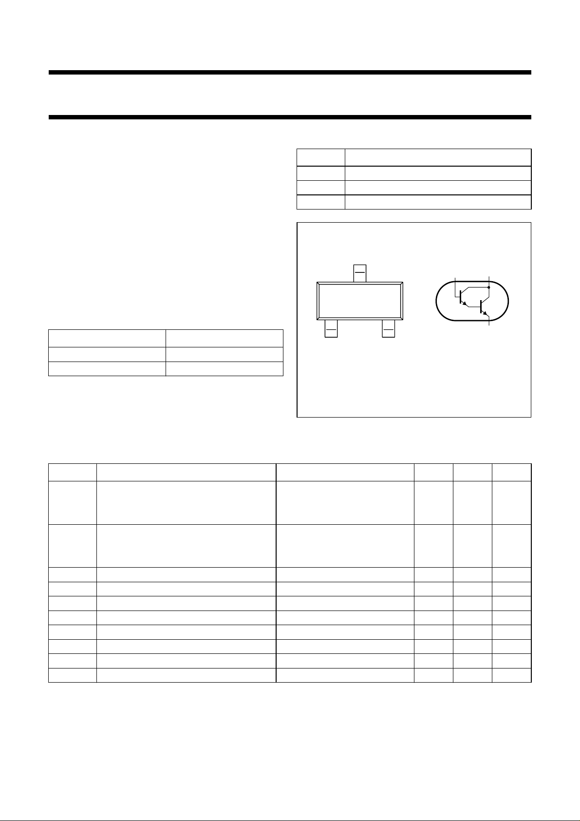
PINNING
PIN DESCRIPTION
1 base
2 emitter
3 collector
handbook, halfpage
Top view
1
3
2
Fig.1 Simplified outline (SOT23) and symbol.
13
TR1
TR2
2
MAM298
LIMITING VALUES
In accordance with the Absolute Maximum Rating System (IEC 134).
SYMBOL PARAMETER CONDITIONS MIN. MAX. UNIT
V
CBO
collector-base voltage open emitter
BCV27 − 40 V
BCV47 − 80 V
V
CES
collector-emitter voltage open base
BCV27 − 30 V
BCV47 − 60 V
V
I
I
I
P
T
T
T
EBO
C
CM
B
tot
stg
j
amb
emitter-base voltage open collector − 10 V
collector current (DC) − 500 mA
peak collector current − 800 mA
base current − 100 mA
total power dissipation T
≤ 25 °C; note 1 − 250 mW
amb
storage temperature −65 +150 °C
junction temperature − 150 °C
operating ambient temperature −65 +150 °C
Note
1. Transistor mounted on an FR4 printed-circuit board.
1999 Apr 08 2

Philips Semiconductors Product specification
NPN Darlington transistors BCV27; BCV47
THERMAL CHARACTERISTICS
SYMBOL PARAMETER CONDITIONS VALUE UNIT
R
th j-a
Note
1. Transistor mounted on an FR4 printed-circuit board.
CHARACTERISTICS
=25°C unless otherwise specified.
T
amb
SYMBOL PARAMETER CONDITIONS MIN. TYP. MAX. UNIT
I
CBO
I
EBO
h
FE
V
CEsat
V
BEsat
V
BEon
f
T
thermal resistance from junction to ambient note 1 500 K/W
collector cut-off current
BCV27 I
BCV47 I
= 0; V
E
= 0; V
E
=30V −−100 nA
CBO
=60V −−100 nA
CBO
emitter cut-off current IE= 0; VEB=10V −−100 nA
DC current gain VCE= 5 V; (see Fig.2)
BCV27 I
DC current gain V
BCV47 I
= 1 mA 4000 −−
C
I
= 10 mA 10000 −−
C
I
= 100 mA 20000 −−
C
= 5 V; (see Fig.2)
CE
= 1 mA 2000 −−
C
I
= 10 mA 4000 −−
C
I
= 100 mA 10000 −−
C
collector-emitter saturation voltage IC= 100 mA; IB= 0.1 mA −−1V
base-emitter saturation voltage IC= 100 mA; IB= 0.1 mA −−1.5 V
base-emitter on-state voltage IC= 10 mA; VCE=5V −−1.4 V
transition frequency IC= 30 mA; VCE= 5 V; f = 100 MHz − 220 − MHz
1999 Apr 08 3
 Loading...