

Page 1
DATA SH EET
DISCRETE SEMICONDUCTORS
M3D173
BC856T; BC857T series
PNP general purpose transistors
Product data sheet
Supersedes data of 1999 Apr 26
2000 Nov 15
Page 2
NXP Semiconductors Product data sheet
PNP general purpose transistors
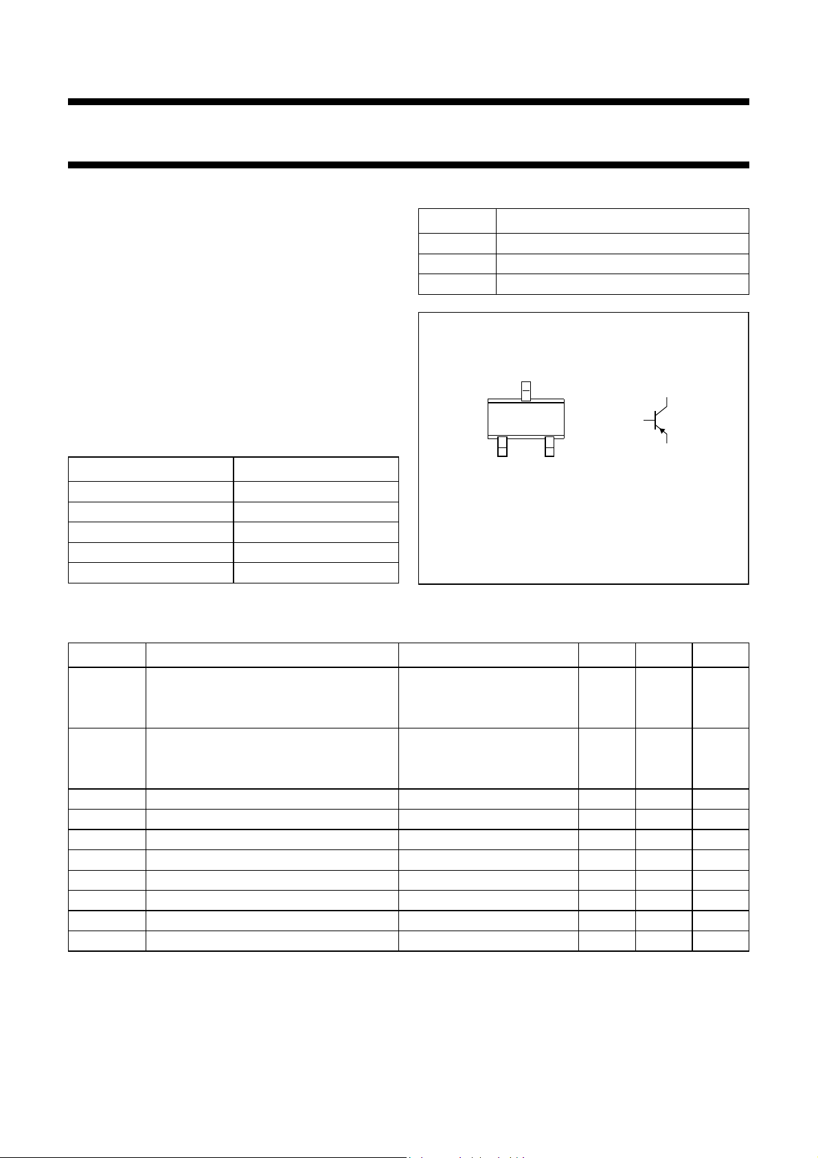
FEATURES
• Low current (max. 100 mA)
• Low voltage (max. 65 V).
APPLICATIONS
• General purpose switching and amplification, especially
in portable equipment.
DESCRIPTION
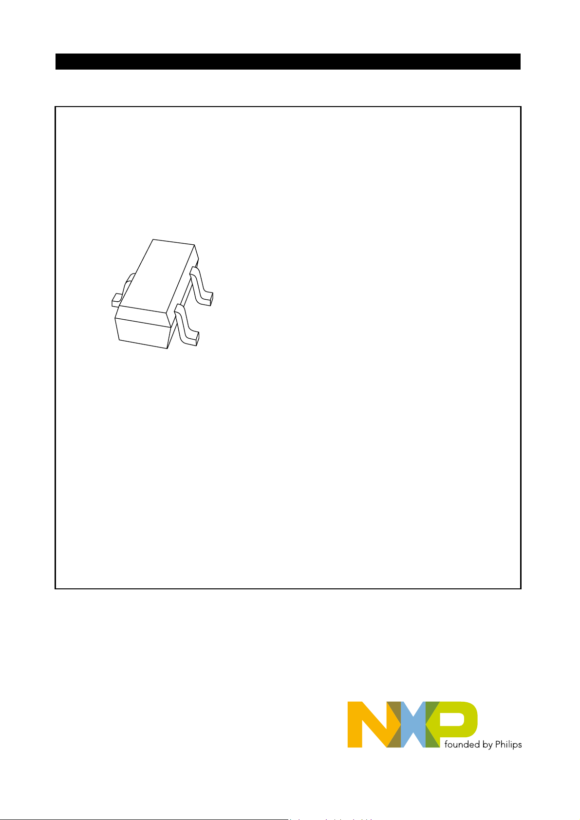
PNP transistor in an SC-75 (SOT416) plastic package.
complements: BC846T; BC847T series.
NPN
MARKING
TYPE NUMBER MARKING CODE
BC856AT 3A
BC856BT 3B
BC857AT 3E
BC857BT 3F
BC857CT 3G
BC856T; BC857T
PINNING
PIN DESCRIPTION
1 base
2 emitter
3 collector
handbook, halfpage
1
Top view
Fig.1 Simplified outline (SC-75; SOT416) and
symbol.
3
1
2
series
3
2
MAM362
LIMITING VALUES
In accordance with the Absolu te Maximum Rating System (IEC 60134).
SYMBOL PARAMETER CONDITIONS MIN. MAX. UNIT
V
CBO
collector-base voltage open emitter
BC856AT; BC856BT − −80 V
BC857AT; BC857BT; BC857CT − −50 V
V
CEO
collector-emitter voltage open base
BC856AT; BC856BT − −65 V
BC857AT; BC857BT; BC857CT − −45 V
V
I
I
I
P
T
T
T
EBO
C
CM
BM
tot
stg
j
amb
emitter-base voltage open collector − −5 V
collector current (DC) − −100 mA
peak collector current − −200 mA
peak base current − −100 mA
total power dissipation T
≤ 25 °C; note 1 − 150 mW
amb
storage temperature −65 +150 °C
junction temperature − 150 °C
operating ambient temperature −65 +150 °C
Note
1. Transistor mounted on an FR4 printed-circuit board.
2000 Nov 15 2
Page 3
NXP Semiconductors Product data sheet
PNP general purpose transistors BC856T; BC857T series
THERMAL CHARACTERISTICS
SYMBOL PARAMETER CONDITIONS VALUE UNIT
R
th j-a
Note
1. Transistor mounted on an FR4 printed-circuit board.
CHARACTERISTICS
T
= 25 °C unless otherwise specified.
amb
SYMBOL PARAMETER CONDITIONS MIN. TYP. MAX. UNIT
I
CBO
I
EBO
h
FE
V
CEsat
V
BE
C
c
C
e
f
T
F noise figure IC = −200 μA; VCE = −5 V;
thermal resistance from junction to ambient in free air; note 1 833 K/W
collector-base cut-off curren t VCB = −30 V; IE = 0 − − −15 nA
VCB = −30 V; IE = 0; Tj = 150 °C − − −5 μA
emitter cut-off current VEB = −5 V; IC = 0 − − −100 nA
DC current gain VCE = −5 V; IC = −2 mA
BC856AT; BC857AT 125 − 250
BC856BT; BC857BT 220 − 475
BC857CT 420 − 800
collector-emitter saturation
voltage
IC = −10 mA; IB = −0.5 mA − − −200 mV
IC = −100 mA; IB = −5 mA; note 1 − − −400 mV
base-emitter voltage IC = −2 mA; VCE = −5 V −580 − −700 mV
IC = −10 mA; VCE = −5 V − − −770 mV
collector capacitance VCB = −10 V; f = 1 MHz; IE = ie = 0 − − 2.5 pF
emitter capacitance VEB = −0.5 V; f = 1 MHz; IC = ic = 0 − 10 − pF
transition frequency IC = −10 mA; VCE = −5 V;
= 100 MHz
f
100 − − MHz
− − 10 dB
= 2 kΩ; f = 1 kHz; B = 200 Hz
R
S
Note
1. Pulse test: tp ≤ 300 μs; δ ≤ 0.02.
2000 Nov 15 3
Page 4
NXP Semiconductors Product data sheet
PNP general purpose transistors BC856T; BC857T series
GRAPHICAL INFORMATION BC857AT
500
handbook, halfpage
h
FE
400
300
200
100
0
−10−2−10
VCE = −5 V.
(1) T
= 150 °C.
amb
(2) T
= 25 °C.
amb
(3) T
= −55 °C.
amb
Fig.2 DC current gain; typical values.
(1)
(2)
(3)
−1
−1 −10 − 102−10
MGT711
IC (mA)
−1200
handbook, halfpage
V
BE
(mV)
MGT712
−1000
−800
(1)
(2)
−600
−400
(3)
−200
3
0
−10−2−10
−1
−1 −10 − 102−10
3
IC (mA)
VCE = −5 V.
(1) T
= −55 °C.
amb
(2) T
= 25 °C.
amb
(3) T
= 150 °C.
amb
Fig.3 Base-emitter voltage as a function of
collector current; typical values.
4
−10
handbook, halfpage
V
CEsat
(mV)
3
−10
2
−10
−10
−1
−10
(1)
(2)(3)
−1 − 10 − 10
MGT713
2
IC (mA)
IC/IB = 20.
(1) T
= 150 °C.
amb
(2) T
= 25 °C.
amb
= −55 °C.
(3) T
amb
Fig.4 Collector-emitter saturation voltage as a
function of collector current; typical values.
−10
−1200
handbook, halfpage
V
BEsat
(mV)
−1000
−800
−600
(1)
(2)
(3)
MGT714
−400
−200
0
3
−10
−1
−1 − 10 − 10
2
−10
3
IC (mA)
IC/IB = 20.
(1) T
= −55 °C.
amb
(2) T
= 25 °C.
amb
= 150 °C.
(3) T
amb
Fig.5 Base-emitter saturation voltage as a
function of collector current; typical values.
2000 Nov 15 4
Page 5
NXP Semiconductors Product data sheet
PNP general purpose transistors BC856T; BC857T series
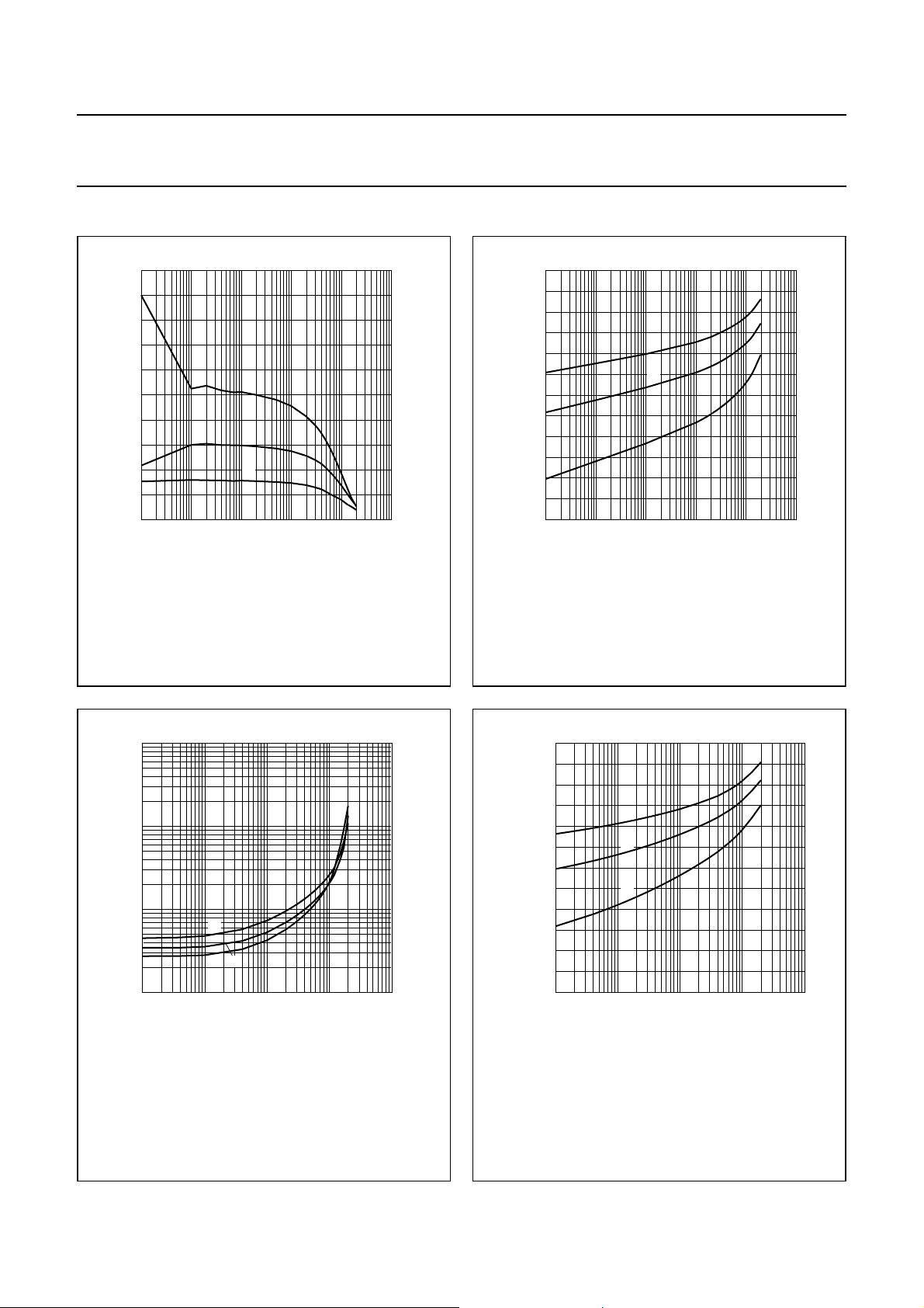
GRAPHICAL INFORMATION BC857BT
1000
handbook, halfpage
h
FE
800
600
400
200
0
−10−2−10
VCE = −5 V.
(1) T
= 150 °C.
amb
(2) T
= 25 °C.
amb
(3) T
= −55 °C.
amb
Fig.6 DC current gain; typical values.
(1)
(2)
(3)
−1
−1 −10 − 102−10
MGT715
IC (mA)
−1200
handbook, halfpage
V
BE
(mV)
MGT716
−1000
−800
(1)
(2)
−600
−400
(3)
−200
0
3
−10
−2
−10
−1
−1 −10 − 102−10
3
IC (mA)
VCE = −5 V.
(1) T
= −55 °C.
amb
(2) T
= 25 °C.
amb
(3) T
= 150 °C.
amb
Fig.7 Base-emitter voltage as a function of
collector current; typical values.
4
−10
handbook, halfpage
V
CEsat
(mV)
3
−10
2
−10
−10
−1
−10
(1)
(3)
(2)
−1 − 10 − 10
MGT717
2
IC (mA)
IC/IB = 20.
(1) T
= 150 °C.
amb
(2) T
= 25 °C.
amb
= −55 °C.
(3) T
amb
Fig.8 Collector-emitter saturation voltage as a
function of collector current; typical values.
−10
−1200
handbook, halfpage
V
BEsat
(mV)
MGT718
−1000
−800
(1)
(2)
−600
(3)
−400
−200
0
3
−10
−1
−1 − 10 − 10
2
−10
3
IC (mA)
IC/IB = 20.
(1) T
= −55 °C.
amb
(2) T
= 25 °C.
amb
= 150 °C.
(3) T
amb
Fig.9 Base-emitter saturation voltage as a
function of collector current; typical values.
2000 Nov 15 5
Page 6
NXP Semiconductors Product data sheet
PNP general purpose transistors BC856T; BC857T series
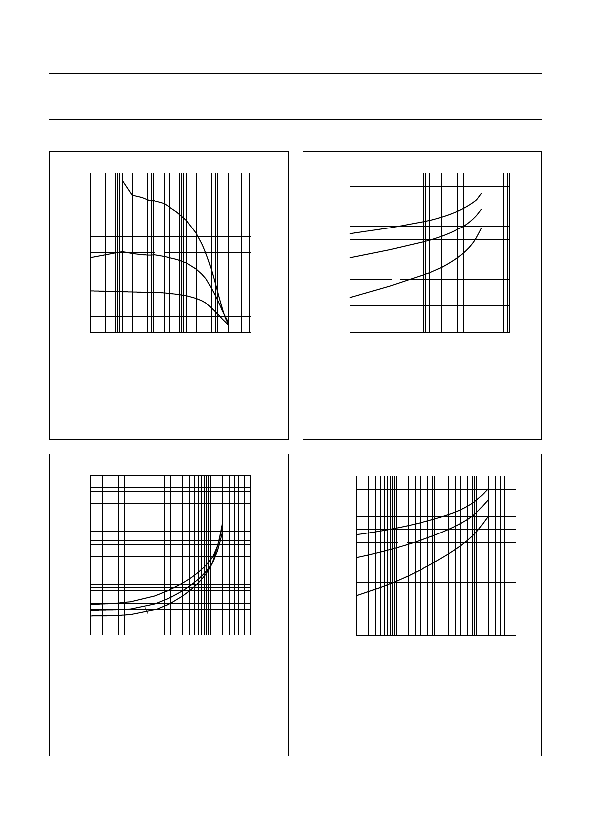
GRAPHICAL INFORMATION BC857CT
1000
handbook, halfpage
h
FE
800
600
400
200
0
−10−2−10
VCE = −5 V.
(1) T
= 150 °C.
amb
(2) T
= 25 °C.
amb
(3) T
= −55 °C.
amb
Fig.10 DC current gain; typical values.
(1)
(2)
(3)
−1
−1 −10 − 102−10
MGT719
IC (mA)
−1200
handbook, halfpage
V
BE
(mV)
MGT720
−1000
−800
(1)
(2)
−600
−400
(3)
−200
0
3
−10
−1
−1 −10 −10
2
−10
3
IC (mA)
VCE = −5 V.
(1) T
= −55 °C.
amb
(2) T
= 25 °C.
amb
(3) T
= 150 °C.
amb
Fig.11 Base-emitter voltage as a function of
collector current; typical values.
4
−10
handbook, halfpage
V
CEsat
(mV)
3
−10
2
−10
−10
−1
−10
(1)
(2)
(3)
−1 − 10 − 10
MGT721
2
IC (mA)
IC/IB = 20.
(1) T
= 150 °C.
amb
(2) T
= 25 °C.
amb
= −55 °C.
(3) T
amb
Fig.12 Collector-emitter saturation voltage as a
function of collector current; typical values.
−10
−1200
handbook, halfpage
V
BEsat
(mV)
MGT722
−1000
−800
(1)
(2)
−600
(3)
−400
−200
3
0
−10
−1
−1 − 10 − 10
2
−10
3
IC (mA)
IC/IB = 20.
(1) T
= −55 °C.
amb
(2) T
= 25 °C.
amb
= 150 °C.
(3) T
amb
Fig.13 Base-emitter satur ation v oltag e as a
function of collector current; typical values.
2000 Nov 15 6
Page 7
NXP Semiconductors Product data sheet
6
PNP general purpose transistors BC856T; BC857T series
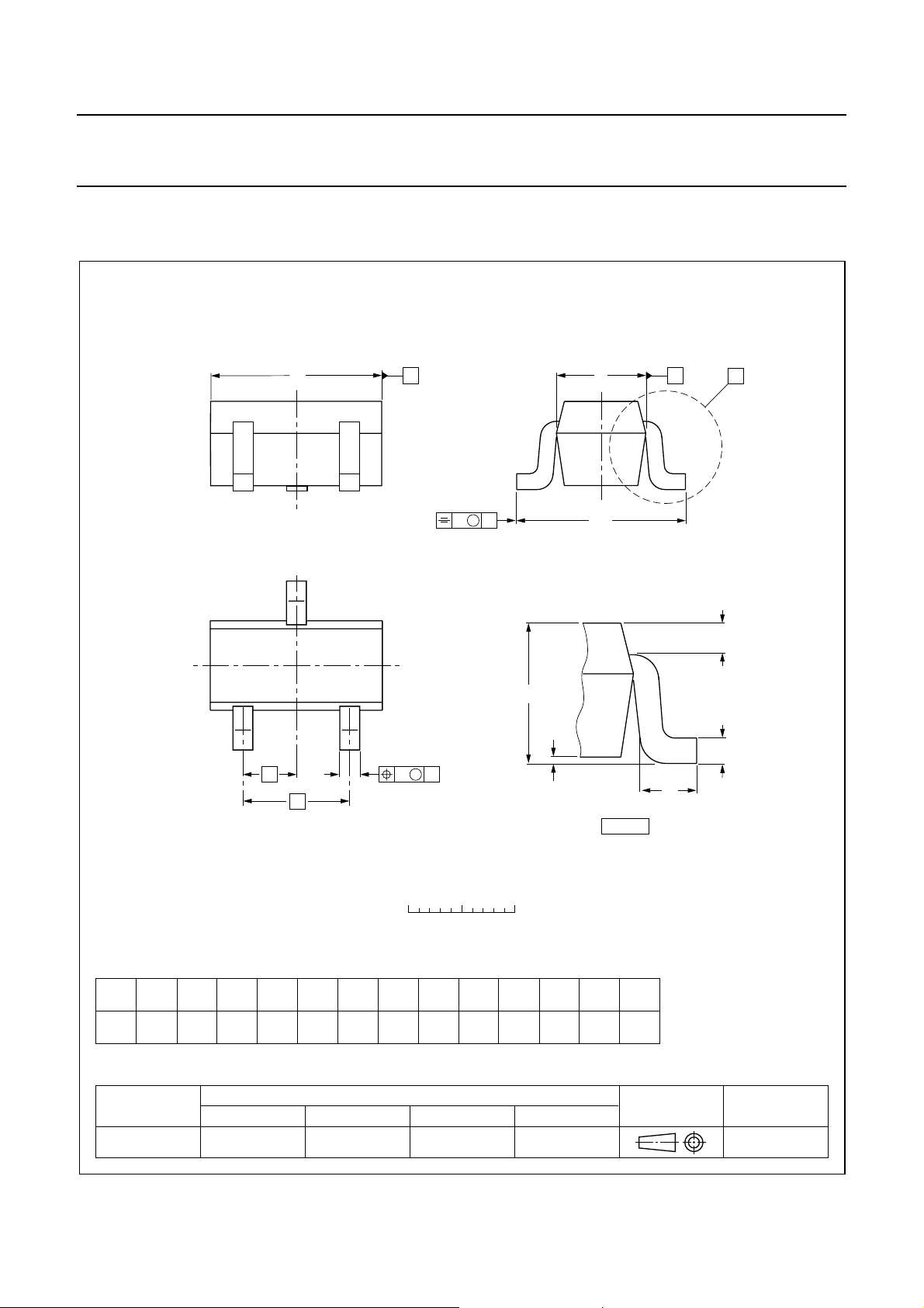
PACKAGE OUTLINE
Plastic surface mounted package; 3 leads SOT41
D
v
M
A
3
12
e
b
1
p
e
w
M
B
E
H
E
A
A
1
detail X
AB
L
p
X
Q
c
0 0.5 1 mm
scale
DIMENSIONS (mm are the original dimensions)
A
1
UNIT
A
0.95
mm
0.60
OUTLINE
VERSION
SOT416 SC-75
max
0.1
b
cD
p
0.30
0.25
0.10
1.8
1.4
0.15
IEC JEDEC EIAJ
E
0.9
0.7
REFERENCES
e
e
H
L
1
1.75
0.5
1
1.45
p
E
0.45
0.23
0.15
0.13
v
Qw
0.2
0.2
EUROPEAN
PROJECTION
ISSUE DATE
97-02-28
2000 Nov 15 7
Page 8

NXP Semiconductors Product data sheet
PNP general purpose transistors BC856T; BC857T series
DATA SHEET STATUS
DOCUMENT
STATUS
Objective data sheet Development This document contains data from the objective specification for product
Preliminary data sheet Qualification This document contains data from the preliminary specification.
Product data sheet Production This document contains the product specification.
Notes
1. Please consult the most recently issued document before initiating or co mpleting a design.
2. The product status of device(s) described in this document may have changed since this document was published
and may differ in case of multiple devices. The latest product status information is available on the Internet at
http://www.nxp.com.
URL
DISCLAIMERS
General ⎯ Information in this document is believed to be
accurate and reliable. However, NXP Semiconductors
does not give any representations or warranties,
expressed or implied, as to the accuracy or completeness
of such information and shall have no liability for the
consequences of use of such information.
Right to make changes ⎯ NXP Semiconductors
reserves the right to make changes to information
published in this document, including without limitation
specifications and product descriptions, at any time and
without notice. This document supersedes and replaces all
information supplied prior to the publication hereof.
Suitability for use ⎯ NXP Semiconductors products are
not designed, authorized or warranted to be su itable for
use in medical, military, aircraft, space or life support
equipment, nor in applications where failure or malfunction
of an NXP Semiconductors product can reasonably be
expected to result in personal injury, death or severe
property or environmental damage. NXP Semiconductors
accepts no liability for inclusion and/or use of NXP
Semiconductors products in such equipment or
applications and therefore such inclusion and/or use is at
the customer’s own risk.
Applications ⎯ Applications that are described herein for
any of these products are for illustrative purposes only.
NXP Semiconductors makes no representation or
warranty that such applications will be suitable for the
specified use without further testing or modificati on .
(1)
PRODUCT
STATUS
(2)
DEFINITION
development.
above those given in the Characteristics sections of this
document is not implied. Exposure to limiting values for
extended periods may affect device reliability.
Terms and conditions of sale ⎯ NXP Semiconductors
products are sold subject to the general terms and
conditions of commercial sale, as published at
http://www.nxp.com/profile/terms, including those
pertaining to warranty, intellectual property rights
infringement and limitation of liability, unless explicitly
otherwise agreed to in writing by NXP Semiconductors. In
case of any inconsistency or conflict between information
in this document and such terms and conditions, the latter
will prevail.
No offer to sell or license ⎯ Nothing in this document
may be interpreted or construed as an offer to sell products
that is open for acceptance or the grant, conveya nce or
implication of any license under any copyrights, patents or
other industrial or intellectual property rights.
Export control ⎯ This document as well as the item(s)
described herein may be subject to export control
regulations. Export might require a prior authorization from
national authorities.
Quick reference data ⎯ The Quick reference data is an
extract of the product data given in the Limiting values and
Characteristics sections of this document, and as such is
not complete, exhaustive or legally binding.
Limiting values ⎯ Stress above one or more limiting
values (as defined in the Absolute Maximum Ratings
System of IEC
the device. Limiting values are stress ratings only an d
operation of the device at these or any other conditions
2000 Nov 15 8
60134) may cause permanent damage to
Page 9

NXP Semiconductors
Customer notification
This data sheet was changed to reflect the new company name NXP Semiconductors . No changes were
made to the content, except for the legal definitions and disclaimers.
Contact information
For additional information please visit: http://www.nxp.com
For sales offices addresses send e-mail to: [email protected]
© NXP B.V. 2009
All rights are reserved. Reproduction in whole or in part is prohibited without the prior written consent of the copyright owner.
The information presented in this documen t d oes not form part of any quotation or contract, is believed to be a ccur ate a nd re li a ble and may be chan ged
without notice. No liability will be accepted by the publisher for any consequence of its use. Publication thereof does not convey nor imply any license
under patent- or other industri al or intellectual property rights.
Printed in The Netherlands 613514/03/pp9 Date of release: 2000 Nov 15 Document order number: 9397 750 07525
 Loading...