

Philips BC847B-TH, BC847C, BC847B, BC847 Datasheet
DATA SH EET
Product specification
Supersedes data of 1997 Mar 12
1999 Apr 23
DISCRETE SEMICONDUCTORS
BC846; BC847
NPN general purpose transistors
ook, halfpage
M3D088
1999 Apr 23 2
Philips Semiconductors Product specification
NPN general purpose transistors BC846; BC847
FEATURES
• Low current (max. 100 mA)
• Low voltage (max. 65 V).
APPLICATIONS
• General purpose switching and amplification.
DESCRIPTION
NPN transistor in a SOT23 plastic package.
PNP complements: BC856 and BC857.
MARKING
Note
1. ∗ = p : Made in Hong Kong.
∗ = t : Made in Malaysia.
TYPE
NUMBER
MARKING
CODE
TYPE
NUMBER
MARKING
CODE
(1)
BC846 1D∗ BC847A 1E∗
BC846A 1A∗ BC847B 1F∗
BC846B 1B∗ BC847C 1G∗
BC847 1H*
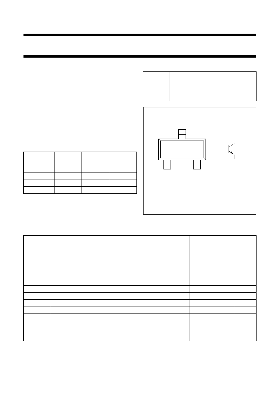
PINNING
PIN DESCRIPTION
1 base
2 emitter
3 collector
Fig.1 Simplified outline (SOT23) and symbol.
handbook, halfpage
21
3
MAM255
Top view
2
3
1
LIMITING VALUES
In accordance with the Absolute Maximum Rating System (IEC 134).
Note
1. Transistor mounted on an FR4 printed-circuit board.
SYMBOL PARAMETER CONDITIONS MIN. MAX. UNIT
V
CBO
collector-base voltage open emitter
BC846 − 80 V
BC847 − 50 V
V
CEO
collector-emitter voltage open base
BC846 − 65 V
BC847 − 45 V
V
EBO
emitter-base voltage open collector − 6V
I
C
collector current (DC) − 100 mA
I
CM
peak collector current − 200 mA
I
BM
peak base current − 200 mA
P
tot
total power dissipation T
amb
≤ 25 °C; note 1 − 250 mW
T
stg
storage temperature −65 +150 °C
T
j
junction temperature − 150 °C
T
amb
operating ambient temperature −65 +150 °C
1999 Apr 23 3
Philips Semiconductors Product specification
NPN general purpose transistors BC846; BC847
THERMAL CHARACTERISTICS
Note
1. Transistor mounted on an FR4 printed-circuit board.
CHARACTERISTICS
T
j
=25°C unless otherwise specified.
Notes
1. V
BEsat
decreases by about 1.7 mV/K with increasing temperature.
2. VBE decreases by about 2 mV/K with increasing temperature.
SYMBOL PARAMETER CONDITIONS VALUE UNIT
R
th j-a
thermal resistance from junction to ambient note 1 500 K/W
SYMBOL PARAMETER CONDITIONS MIN. TYP. MAX. UNIT
I
CBO
collector cut-off current IE= 0; VCB=30V −−15 nA
I
E
= 0; VCB= 30 V; Tj= 150 °C −−5µA
I
EBO
emitter cut-off current IC= 0; VEB=5V −−100 nA
h
FE
DC current gain IC=10µA; VCE=5V;
see Figs 2, 3 and 4
BC846A; BC847A − 90 −
BC846B; BC847B − 150 −
BC847C − 270 −
DC current gain IC= 2 mA; VCE=5V;
see Figs 2, 3 and 4
BC846 110 − 450
BC847 110 − 800
BC846A;BC847A 110 180 220
BC846B; BC847B 200 290 450
BC847C 420 520 800
V
CEsat
collector-emitter saturation
voltage
IC= 10 mA; IB= 0.5 mA − 90 250 mV
I
C
= 100 mA; IB=5mA − 200 600 mV
V
BEsat
base-emitter saturation voltage IC= 10 mA; IB= 0.5 mA; note 1 − 700 − mV
I
C
= 100 mA; IB= 5 mA; note 1 − 900 − mV
V
BE
base-emitter voltage IC= 2 mA; VCE= 5 V; note 2 580 660 700 mV
I
C
= 10 mA; VCE= 5 V; note 2 −−770 mV
C
c
collector capacitance IE=ie= 0; VCB= 10 V; f = 1 MHz; − 2.5 − pF
f
T
transition frequency IC= 10 mA; VCE= 5 V; f = 100 MHz; 100 −−MHz
F noise figure I
C
= 200 µA; VCE=5V; RS=2kΩ;
f = 1 kHz; B = 200 Hz
− 210dB
 Loading...