

Philips BA277 Datasheet
DISCRETE SEMICONDUCTORS
DATA SH EET
M3D319
BA277
Band-switching diode
Product specification
1998 May 06
Philips Semiconductors Product specification
Band-switching diode BA277
FEATURES
• Small plastic SMD package
• Continuous reverse voltage: max. 35 V
• Continuous forward current: max. 100 mA
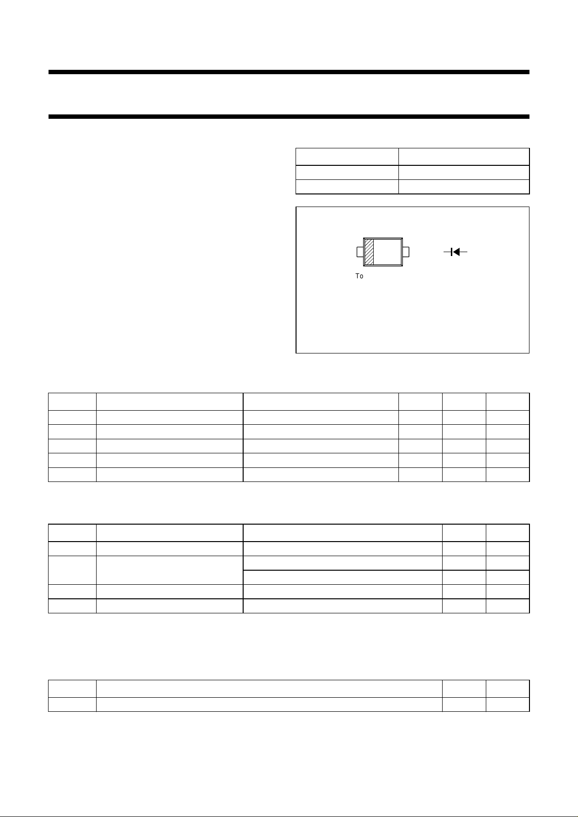
PINNING
PIN DESCRIPTION
1 cathode
2 anode
• Low diode capacitance: max. 1.2 pF
• Low diode forward resistance: max. 0.7 Ω.
APPLICATIONS
handbook, halfpage
12
• Low loss band switching in VHF television tuners.
• Surface mount band-switching circuits.
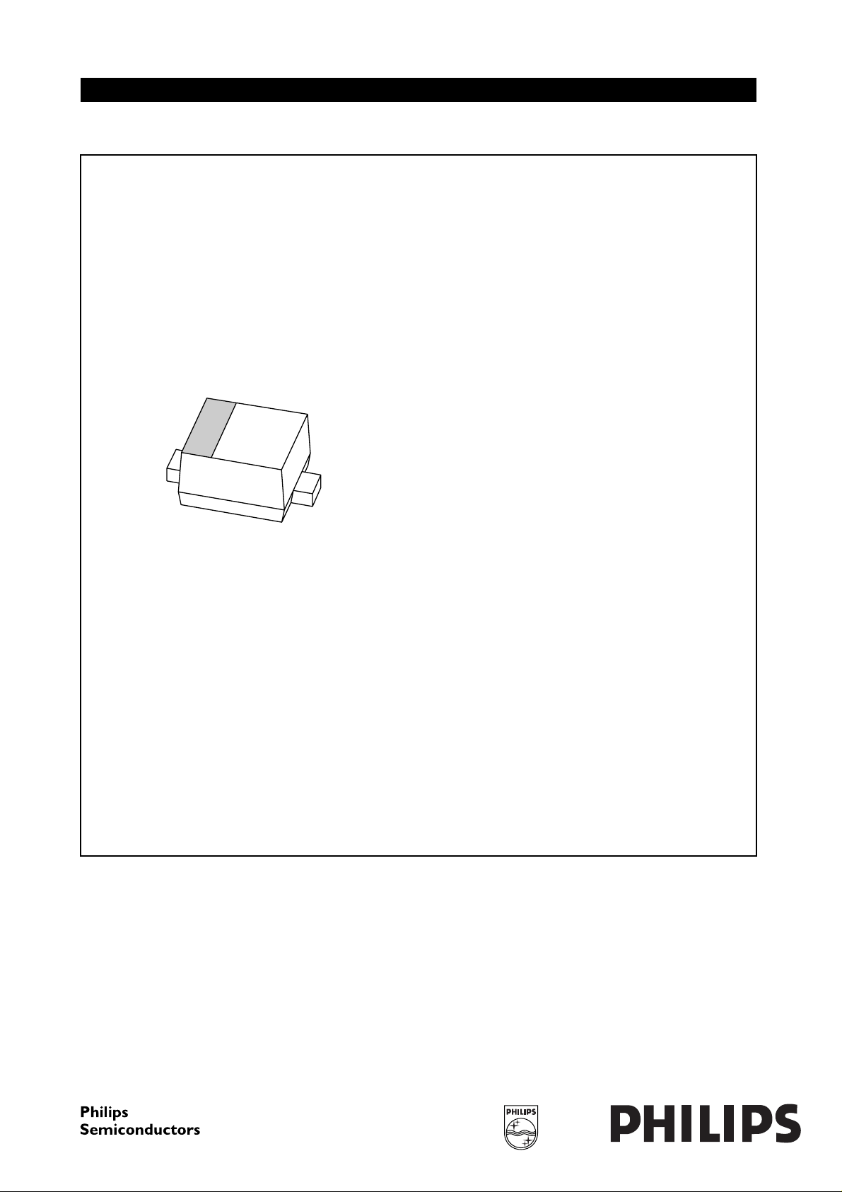
DESCRIPTION
Planar high performance band-switching diode in a small
plastic SOD523 (SC-79) SMD package.
Marking code: 1.
Fig.1 Simplified outline (SOD523; SC-79)
Top view
and symbol.
MAM399
LIMITING VALUES
In accordance with the Absolute Maximum Rating System (IEC 134).
SYMBOL PARAMETER CONDITIONS MIN. MAX. UNIT
V
R
I
F
P
tot
T
stg
T
j
continuous reverse voltage − 35 V
continuous forward current − 100 mA
total power dissipation Ts=90°C − 715 mW
storage temperature −65 +150 °C
junction temperature −65 +150 °C
ELECTRICAL CHARACTERISTICS
T
= 25°C unless otherwise specified.
j
SYMBOL PARAMETER CONDITIONS MAX. UNIT
V
F
I
R
C
d
r
D
forward voltage IF=10mA 1 V
reverse current VR= 25 V 50 nA
V
= 20 V; T
R
=75°C1µA
amb
diode capacitance f = 1 MHz; VR= 6 V; note 1; see Fig.2 1.2 pF
diode forward resistance IF= 2 mA; f = 100 MHz; note 1; see Fig.3 0.7 Ω
Note
1. Guaranteed on AQL basis: inspection level S4, AQL 1.0.
THERMAL CHARACTERISTICS
SYMBOL PARAMETER VALUE UNIT
R
th j-s
thermal resistance from junction to soldering-point 85 K/W
1998 May 06 2
Philips Semiconductors Product specification
Band-switching diode BA277
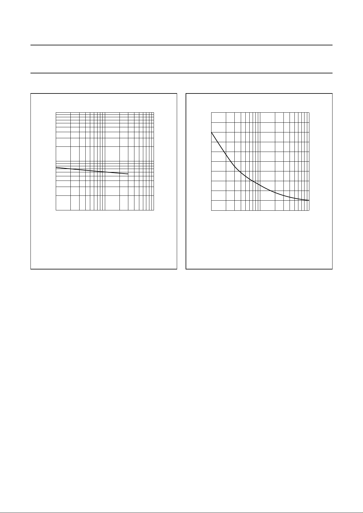
GRAPHICAL DATA
10
handbook, halfpage
C
d
(pF)
1
−1
10
110
f =1 MHz; Tj=25°C.
MGL433
V
(V)
R
Fig.2 Diode capacitance as a function of reverse
voltage; typical values.
2.5
handbook, halfpage
r
D
(Ω)
2.0
1.5
1.0
0.5
2
10
0
−1
10
f = 100 MHz; Tj=25°C.
1
IF (mA)
MGL432
10
Fig.3 Diode forward resistance as a function of
forward current; typical values.
1998 May 06 3
 Loading...