

Page 1

AN1651
Using the NE/SA5234 amplifier
Author: Les Hadley 1991 Oct
INTEGRATED CIRCUITS
Page 2
Philips Semiconductors Application note
AN1651Using the NE/SA5234 amplifier
2
1991 Oct
Author: L. Hadley
I. SUMMARY
The NE/SA5234 is a unique low-voltage quad operational amplifier
specifically designed to operate in a broadly diverse environment. It
is an enhanced pin-for-pin replacement for the LM324 category of
devices. Supply conditions can range from 1.8V to 6.0V with a
resultant current drain of 2.8mA,-700µA per op amp.
Most notable are the input and output dynamic range characteristics
of the individual op amps. The common-mode input voltage can
actually exceed the positive and negative supply rails by 250mV
with no danger of output latching or polarity reversal. In addition, the
output of each op amp will swing to within 50mV of the supply rails
over the full supply range.
The frequency related characteristics are also above average for
low voltage devices in this class. Internal unity gain compensation
makes the NE5234 very resistant to any tendency to oscillate in low
closed-loop gain configurations. Even so, a unity-gain bandwidth of
2.5MHz is retained. Slew rate is 0.8V/µs and each op amp will
settle to a 1% of nominal level within 1.4µs.
II. DETAILED DESCRIPTION
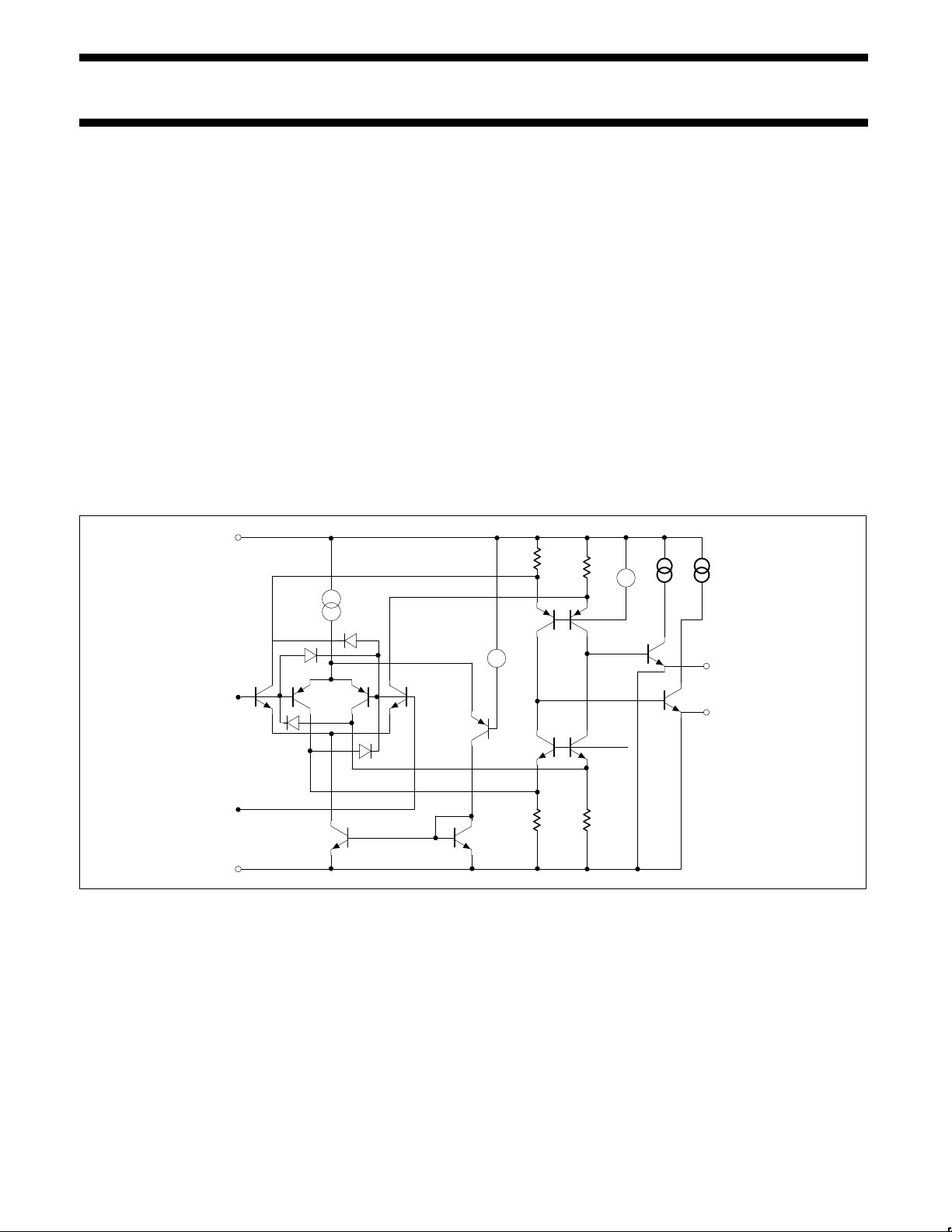
Input Stage
The input differential amplifier consists of a compound transistor
structure of parallel NPN and PNP transistors which account for the
unique over-drive characteristics of the NE5234. Referring to Figure
1, it is seen that the NPN pair, Q1 and Q2, allow the input to
operate in the common-mode input voltage range of 1V above V
EE
.
This region is designated the N-mode region in Figure 3a.
Operation in the common-mode range below 1V transfers the input
stage into the P-mode of operation.
In the N-mode operating condition, collector current from Q1 and Q2
is summed in the output emitter node of Q10 and Q12 respectively.
Q1’s base is the non-inverting input and Q2’s base the inverting
input node for the amplifier.
V
CC
R10
R11
VB2
Q10
Q12
VB1
IB1
Q2
Q4Q3
Q5
SWITCH
Q9
R8 R9
Q6
Q7
Q8
I
P
I
N
V
BIAS
IN(–)
(+)
+
–
Q2
SL00630
Figure 1. NE5234 Input Stage
Linear operation between the two modes is governed by a current
steering circuit consisting of Q5,6 and 7 in conjunction with voltage
reference VB1. Operation in the
N-region of the common-mode range will automatically cause Q5 to
transfer the IB1 current source to Q7 and the NPN transistor pair Q1
and Q2. Operation below the 1V level at the inputs allows the
current from IB1 to be fed directly to Q3 and Q4 emitters giving them
priority in processing the signal and linearizing their transfer
function. (The sum of the NPN and PNP input pair currents remain
constant.)
Operation in the common-mode range near the positive supply rail
would normally cause the input stage NPN transistor’s base
collector junction to become forward biased (base current flow
directly to the collector circuit) reversing the collector current flow
direction. In a conventional op amp, this would have the adverse
effect of reversing the output signal polarity as the operating region
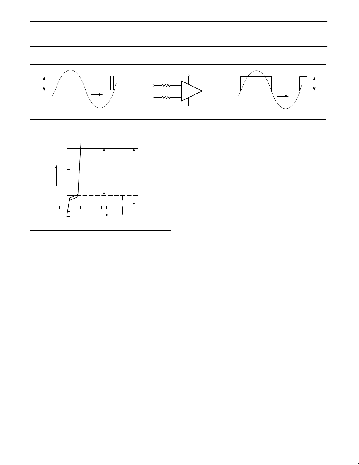
is traversed by the input signal. (see Figure 2)
To prevent this from occurring, large geometry diode-connected
transistors are cross-connected to the opposite NPN collector, (Q1,
Q2). This current, in turn, is summed at the emitter of Q12 pulling it
above the V
CC
rail voltage and preventing polarity reversal. The
inverse condition occurs when Q2 is driven above the positive rail,
with Q10 emitter being pulled up and signal polarity preserved. (See
Figure 1)
Page 3
Philips Semiconductors Application note
AN1651Using the NE/SA5234 amplifier
1991 Oct
3
47k
47k
V
IN
V
OUT
V
CC
+
–
5V
CONVENTIONAL OP AMP PHILIPS NE5234
t
t
V
CC
V
OUT
V
OUT
V
IN
V
IN
V
GND
V
GND
V
GND
V
CC
5V
SL00569
Figure 2. Output Inversion Protection
6
5
4
3
2
1
0.5
-1
-0.1
+0.1
“N-MODE”
CMRR
V
EE
+1 < VCM < V
CC
“LARGE
SIGNAL”
CMRR
“N-MODE”
CMRR
V
EE
< VCM < VEE+0.5V
V
EE
V
OS
mV
COMMON MODE VOLTAGE (VOLTS)
NE5234 Common-Mode Operating Regions
SL00631
Figure 3.
For negative going input signals, which drive the inputs toward the
V
EE
rail and below, another set of diode-connected transistors come
into operation. These steer the current from the input into Q8 or Q9
emitter circuits again preventing the reversal effect.
Figure 3 shows graphically how the N and P mode transitions relate
to the common-mode input voltage and the offset voltage V
OS
.
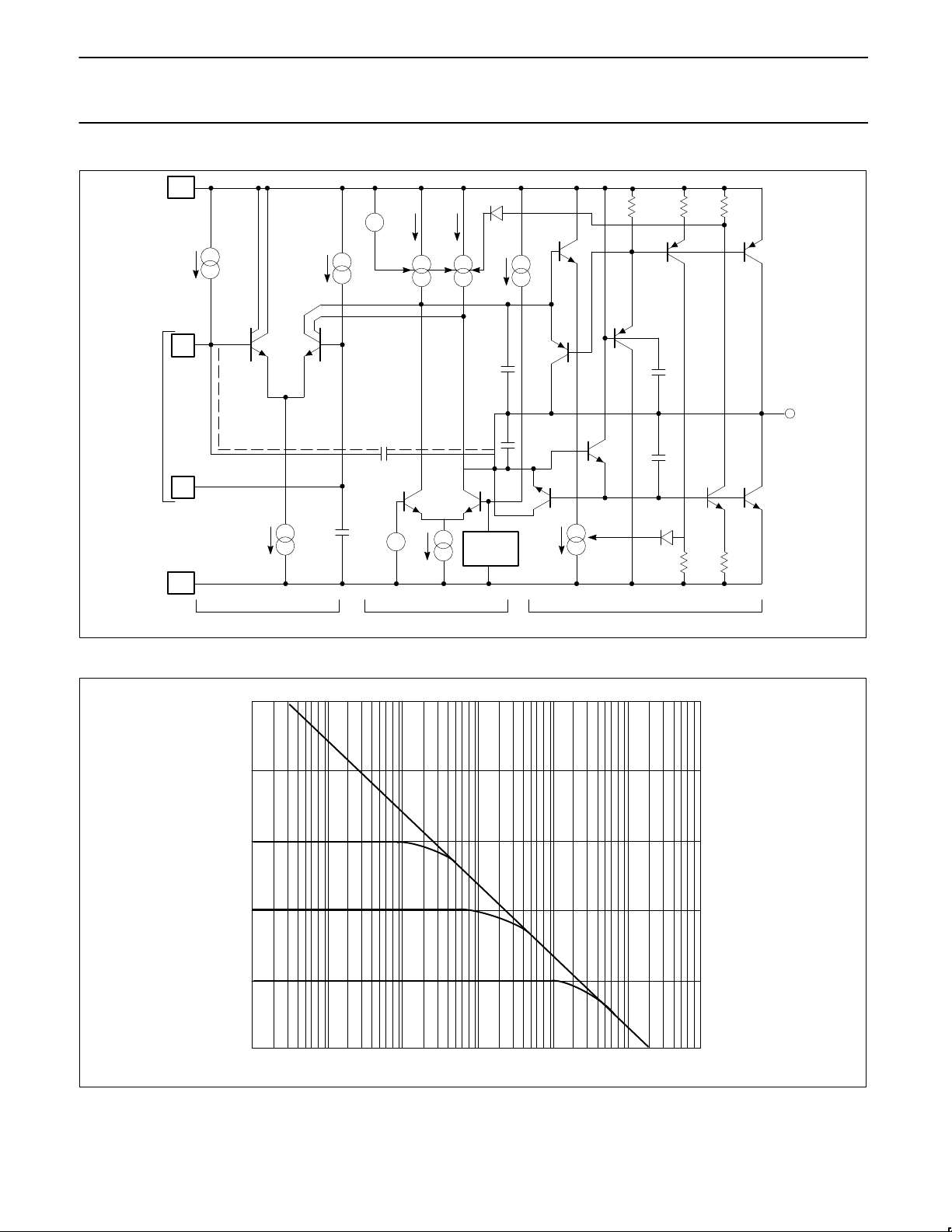
Intermediate Amplifier and Output Stage
(Figure 4)
The intermediate stage is isolated from the input amplifier by emitter
followers
to prevent any adverse loading effect. This stage adds gain to the
over all amplifier and translates levels for the following class-AB
current-control driver. Note that I
2
is the inverting input and I1 the
non-inverting input. The output is taken from multiple collectors on
the non-inverting side and provides matching for the following stage.
Class-AB control of the output stage is achieved by Q61 and Q62
with the associated output current regulators. These act to monitor
the smallest current of the non-load supporting output transistor to
keep it in conduction. Thus, neither Q71 or Q81 is allowed to cutoff
but is forced to remain in the proper Class-AB region.
Overload protection is provided by monitor circuits consisting of
R76-D2 for sinking and R86-D3 for sourcing condition at the output.
When the output current, source or sink, reaches 15 milliamperes,
drive current to the stage is shunted away from current sources IB6
or IB9 reducing base current to driver transistors Q72 and Q82
respectively.
The prevention of saturation in the output stage is achieved by
saturation detectors Q78 and Q88. When either Q71 or Q81
approaches saturation, current is shunted away from the driver
transistors, Q72 or Q83 respectively.
III. CHARACTERISTICS
Internal Frequency Compensation
The use of nested Miller capacitors C2 through C6, in the
intermediate and output sections, provides the overall frequency
compensation for the amplifier. The dominant pole setting capacitor,
C2, provides a constant 6dB/octave roll-off to below the unity gain
frequency of 2.5MHz. Figure 5 shows the measured frequency
response plot for various values of closed-loop gains.
Page 4
Philips Semiconductors Application note
AN1651Using the NE/SA5234 amplifier
1991 Oct
4
D2
I
B2
I
B4
I
B5
I
B6
I
B8
I
B7
I
B9
I
B3
V
B4
V
CC
I
2
I
1
V
EE
D3
CLASS
AB
CONTROL
Q61 Q62
Q83
Q85
Q81
Q82
Q71
Q75
Q72
Q78
Q53,54
Q51,52
C1
C2
C3
C4
C5
R82
C6
Q84
OUTPUT
INPUT
+
–
INTERMEDIATE STAGE CURRENT CONTROL CLASS AB OUTPUT
R85 R76
R86 R75
SL00632
Figure 4.
dB
100
80
60
40
20
0
10Hz 100Hz 1kHz 10kHz 100kHz 1MHz
FREQUENCY
10 10
6
G1000
SL00633
Figure 5. NE5234 Closed Loop Gain vs Frequency
Page 5
Philips Semiconductors Application note
AN1651Using the NE/SA5234 amplifier
1991 Oct
5
4
11
+
–
47k
5234
100
x10
HP
3585
SPECTRUM
ANALYZER
10Ω
600Ω
+2.5V
–2.5V
SL00634
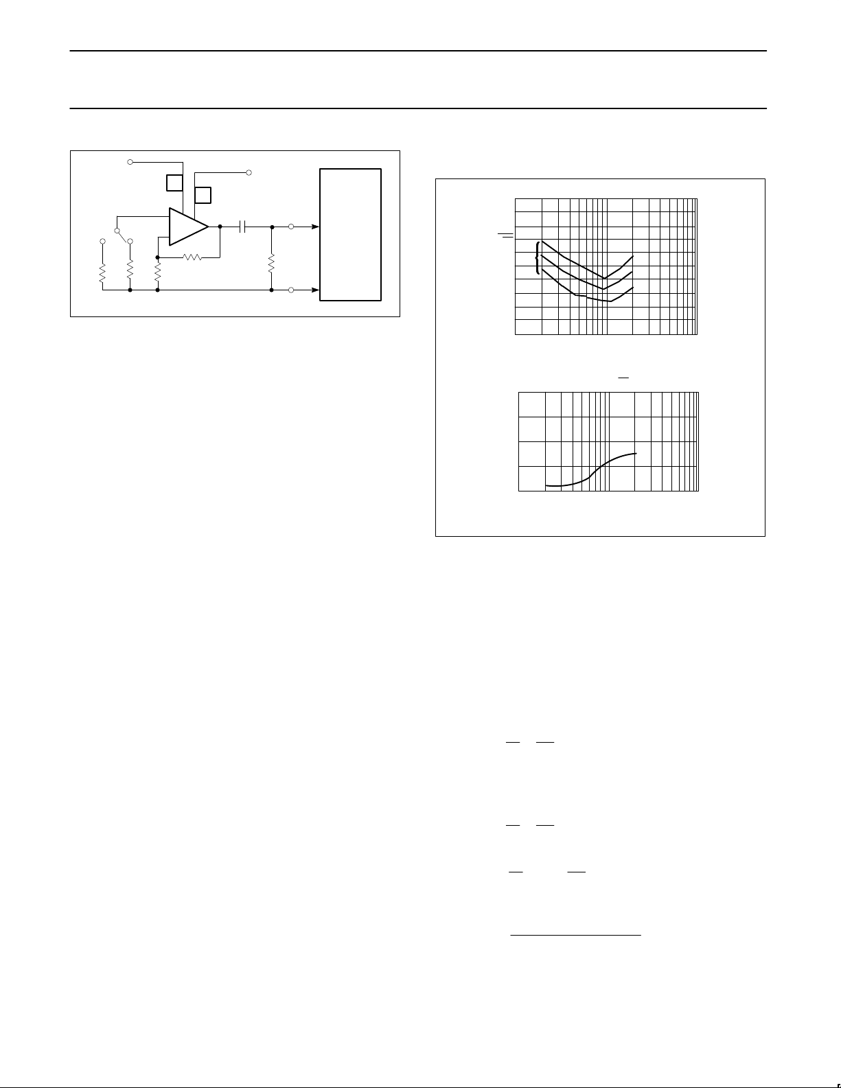
Figure 6. Noise Test Circuit
IV. NOISE REFERRED TO THE INPUT
The typical spectral voltage noise referred to each of the op amps in
the NE/SA5234 is specified to be 25nV/√Hz. Current noise is not
specified. In the interest of providing a balance of information on the
device parameters, a small sample of the standard NE5234s, were
tested for input noise current. While this data does not represent a
specification, it will give the designer a ball park figure to work with
when beginning a particular design with the device. For
completeness I have provided the corresponding spectral noise
voltage data for the same sample. The data was taken using an
HP3585A spectrum analyzer which has the capability of reading
noise in nV/√Hz.
The test circuit is shown in Figure 6. As is typical for such
measurements the amplifier under test is terminated at its input first
with a very low resistance, for the voltage noise reading, followed by
the same test with a high value of resistance to register the effect of
current noise. The amplifier is set to a non-inverting
closed-loop gain of 20dB. Dual supply operation was chosen to
allow direct termination of the input resistors to ground.
The measurements were made over the range from 200Hz to 2kHz.
Each sample is measured at 200Hz, 500Hz, 1kHz and 2kHz. The
data is averaged for each frequency and then the small sample
distribution is derived statistically giving the standard deviation
relative to the mean.
Referring to the graph in Figure 7a, the equivalent voltage noise is
seen to average 18 nV/√Hz. The 95% confidence interval is
determined to be approximately one nV/√Hz. The majority of the
errors which contribute to this measurement are due to the thermal
noise of the parallel combination of the feedback resistor network, in
addition to the 10Ω termination resistor on the non-inverting input.
At 300° Kelvin a 10Ω resistor generates 0.4 nV/√Hz and the
feedback network’s equivalent resistance of 90Ω generates
1.2nV/√Hz. Their order-of-magnitude difference from the main noise
sources allows them to be neglected in the overall calculation of
total stage noise.
Noise current is measured across a 47kΩ resistor and averaged in
the same manner. The thermal noise generated by this large
resistance is not insignificant. At room temperature it is 28nV/√Hz
and must be subtracted from the total noise as measured at the
output of the op amp in order to arrive at the equivalent current
generated noise voltage. Figure 7b shows the derived current
noise distribution for the small sample of 10 NE5234 devices. The
result shows that noise current in the 200Hz to 2kHz frequency is
typically 0.2pA/√Hz. The 1/f region was not determined for either
current or voltage noise.
95%
INT.
En for RS = 10Ω -nV/Hz
22
19
18
17
16
100 200 2000 10000
nV
Hz
Ǹ
a.
pAńHz
Ǹ
0.5
12
0.1
100
200
1k
2k
10000Hz
f
P
in 10
P
b.
SL00635
Figure 7. Typical Noise Current and Voltage vs Frequency
V. GUIDE LINES FOR MINIMIZING NOISE
When designing a circuit where noise must be kept to a minimum,
the source resistances should be kept low to limit thermally
generated degradation in the overall output response.
Orders-of-magnitude should be kept in mind when evaluating noise
performance of a particular circuit or in planning a new design. For
instance, a transducer with a 10kΩ source resistance will generate
2µV of RMS noise over a 20kHz bandwidth. Using the graphical
data above, total noise from a gain stage may be calculated.-
25nVń Hz
Ǹ
@ BWǸ+ 3.5V
RMS
(EQ. 1.)
Amplifier Noise Voltage
BW + 10kHz
Noise from source 10kΩ Resistance –
14nVń Hz
Ǹ
@ BWǸ+ 20V
RMS
(EQ. 2.)
Noise Voltage from source resistance
0.2pAń Hz
Ǹ
@ 103@ BWǸ+ 0.28V
RMS
(EQ. 3.)
Current generated noise
The total noise is the root-to-sum-of-the-squares of the individual
noise voltages –
+
)
)
Ǹ
(EQ. 4.)
+ 4.04V
RMS
En
(3.5)
2
(2.0)
2
(0.28)
2
To determine the signal-to-noise ratio of the stage we must first
choose a stage gain, make it 40dB, and a signal voltage magnitude
from the transducer which we will set at 10mV
. The resulting
RMS
Page 6
Philips Semiconductors Application note
AN1651Using the NE/SA5234 amplifier
1991 Oct
6
signal-to-noise ratio at the output of this stage is determined by first
multiplying the gain times the signal which gives 1V
RMS
with a
resultant noise of 400mV
RMS
. The signal-to-noise ratio is calculated
as
Sń N 20log
10
(1.0ń 4x10
* 4
) + 68dB
(EQ. 5.)
This is quite adequate for good quality audio applications.
Next assume that the bandwidth is cut to 3.0kHz with an input of
1mV
RMS
. The RMS noise is modified by the ratio of the root of the
noise channel bandwidths.
ƪ
Ǹ
20x10
3
Ǹ
ƫ @ EN + 1.6V
RMS
(EQ. 6.)
ƪ
*
*
ƫ
(EQ. 7.)
+ 56dB
+
–
+
–
1mV
RMS
e
n
x100
R
S
= 100Ω
1.6µV
e
n
x10
100kΩ
1mV
RMS
SIGNAL
SL00636
Figure 8.
UNITY GAIN
+
–
10k
100k
3
2
1
600Ω
2.2µF
1µF
R
L
= 600Ω
V
CC
+
V
CC
2
+
–
3
2
1
10k 10k
+
1k
100pF10k
4.7µF
1µF
1µF
600Ω
V
CC
2
40dB CIRCUIT
ST1700
DISTORTION
ANALYZER
V
CC
ST1700
SL00637
Figure 9. NE5234 THD Test Circuits
VI. MULTIPLE STAGE CONSIDERATIONS
Since multiple noise generators are non-coherent, their total effect is
the root-of-the-sum-of-the-squares of the various noise generators
at a given amplifier input.
This makes orders-of-magnitude lower noise sources less important
than the higher magnitude source. Therefore, when considering the
combined signal-to-noise of multiple stages of gain, the first stage in
a chain dominates making its design parameters the most critical.
For this reason it is good practice to make the preamp stage gain as
high as practical to boost signal levels to the second stage allowing
at least an order-of-magnitude above the second-stage noise. For
instance, a signal input which exceeds the input noise of the
following stage by a factor of 10:1 will only be degraded by 0.5% or
-46dB, neglecting the first-stage noise. If we use the preceding
example with a first-stage output signal of 100mV
RMS
and a 56dB
S/N, and an output noise of 0.16mV . Following this with a 10kHz
band limited gain-of-10 second-stage, with a 100kΩ noise source at
the non-inverting input, the combined S/N is calculated as follows:
(assume a 100Ω source resistance from amplifier #1)
The Second stage output noise is:
3
3x10
Amplified Noise = 160µV
RMS
SńN 20 log
10
100x10
1.6x10
3
4
A 56dB S/N will provide superior voice channel communications .
+1.6mV
RMS
NOISE
Page 7

Philips Semiconductors Application note
AN1651Using the NE/SA5234 amplifier
1991 Oct
7
(EQ. 8.)
ƪ
(0.163x10
* 3)2
)
ǒ
4KT @ 100 @ 10,000
Ǹ
Ǔ
2
Ǹ
ƫ
@ 10
+ 1.6mV
+
+
*
The amplified output signal = 1V
RMS
(EQ. 10.)
Sń N + 20 log
10
ǒ
1
1.6x10
* 3
Ǔ
+ 56dB
UNITY GAIN
3
0
0.1
V
1.0
UNITY GAIN
3
0
0.1
V
1.1
a. b.
LM324
NE5234
UNITY GAIN
0.8
0
0.1
V
1.1
c.
SL00638
VCC = 1.8V
VCC = 2.0V
VCC = 3.0V
Figure 10. THD vs Supply Voltage for 1V
RMS
Output
RL = 600Ω
R
L
= 10kΩ
3
P
0
0.1
V 0.9
THD for VCC = 1.8V
-RL = 10k/600Ω
2.5
0
0.1
V 1.1
VCC = 2V
RL = 10k/600Ω
RL = 600Ω
RL = 10kΩ
c.b.
RL = 10kΩ
VCC = 3.0V
GAIN = 40dB
2
0
0.1
V 1.1
a.
SL00639
Figure 11. THD vs Load
A series of tests are shown to allow you to see just how resistant
this device is to generating clipping distortion. Two different gain
configurations were chosen to demonstrate this particular feature:
unity gain non-inverting and 40dB non-inverting. The test set-up
K
BoltzmanȀsConstant
1.38x10
23
Joule
DegKelvin
(EQ. 9.)
T+300oK ; BW+10kHz
Note that there is no effect from the second-stage thermally
generated resistor noise due to the dominating effect of the
first-stage amplified noise being much greater than the input noise of
the second-stage. In addition the equivalent noise resistance of the
second-stage is essentially the output resistance of the first-stage
plus any series resistance used in coupling the two. This is the
parallel combination of source resistance with input terminating or
biasing resistance.
VII. LOW HARMONIC DISTORTION
The NE/SA5234 is extremely well adapted to reducing harmonic
distortion as it relates to signal level and head room in audio and
instrumentation circuits. Its unique internal design limits overdrive
induced distortion to a level much below that experienced with other
low voltage devices. As will be shown, the device is capable of
operating over a wide supply range without causing the typical
clipping distortion prevalent in companion operational amplifiers of
this class.
was as shown in Figure 9. The Harmonic Distortion analyzer used
to make the measurements was a Storage Technology ST1700.
The test frequency is 1kHz. For single supply operation, as
previously covered, the amplifier should be biased to half the supply
voltage to minimize distortion. Operation with dual supplies is
simpler from a parts count standpoint as isolation capacitors are not
required. Also the time constants associated with charging and
discharging these is eliminated . Figure 10a,b and c shows the total
harmonic distortion in percent versus input voltage level at 1kHz in
V
for a non-inverting, unity gain NE5234. The load on the
RMS
amplifier output is 10kΩ. Beginning with a supply voltage of 1.8V
and an input level of 0.1V
remains there up to an input level just over 0.5V
increases to 0.4% for for 0.6V
For a 2V supply, the input levels increase to 0.65V
0.7V
, respectively for similar levels of distortion. With a supply
RMS
voltage of 3.0V the input may be increased to 1V
rises to 0.2% and 1.1V
, distortion is well below 0.2% ad
RMS
(1.7V
RMS
for only 0.8% THD. Operation with a
RMS
P-P
).
(1.4V
RMS
RMS
before THD
RMS
600Ω load will only raise the THD figures slightly . By way of
comparison, Figure 10c shows the greatly reduced dynamic range
experienced when an LM324 is plugged into the test socket in place
of the NE5234. Note that The THD is completely off scale for the
case of 1.8 and 2.0V supply, then is barely usable for the low level
end of the 3.0V supply example. Figure 11a, b, and c demonstrates
the effect on harmonic distortion when closed loop gain is increased
to 40dB in the non-inverting mode. It is evident that little increase in
THD levels result. The graphs for the 2.0 and 3.0V supply case also
include additional information on the effect of a 600Ω load on
distortion.
and
P-P
) and
Page 8

Philips Semiconductors Application note
AN1651Using the NE/SA5234 amplifier
1991 Oct
8
VIII. GAIN-BANDWIDTH VS CLOSED LOOP FREQUENCY RESPONSE
Figure 5 shows the small signal frequency response of the NE5234
versus closed-loop gain in dB. The test circuit is shown in Figure 6.
The plot is taken from measured data and thus shows how each
value of closed-loop gain coincides with the open-loop response
curve. The NE/SA5234’s open-loop gain response has a uniform
6dB/octave roll-off which continues beyond 2.5MHz. This factor
guarantees each op amp in the IC a high stability in virtually any
gain configuration. In making these measurements, dual supplies of
±2.5V were used in order to allow a grounded reference plane and
no coupling capacitors which might cause frequency related errors.
A critical parameter which affects the reproduction quality of
complex waveforms is the gain-bandwidth-product of the operational
amplifier. Essentially, this is a measure of the maximum frequency
handling characteristics of any operational amplifier for a given
closed-loop gain. As is evident from the graph, the NE/SA5234 has
a 2.5MHz unity gain cross-over frequency — much higher than most
other low voltage op amps. For comparison, the µA741 has a
gain-bandwidth-product of 1MHz, as do the LM324 and the
MC3403.
IX. LOOP-GAIN
The dynamic signal response of any closed-loop amplifier stage is a
function of the Loop-gain of that particular stage. Loop-gain is equal
to the open-loop gain in dB, at a given frequency, minus the
closed-loop gain of the stage. The greater the Loop-gain, the lower
the transfer function error of the device. Essentially, any parametric
error is reduced by the factor of the Loop-gain. This includes output
resistance and output signal voltage accuracy. It is good practice
then to maximize Loop-gain to the degree that stage gain may be
sacrificed for bandwidth. In some cases it is actually better to use
two stages of gain in order to preserve signal quality than to use one
high gain stage. Of course, there is a trade-off between the
aforementioned factors that affect the signal-to-noise ratio of the
stage and optimizing the Loop-gain. For example, a voice-band
audio stage which requires 3kHz bandwidth, should be limited to a
closed-loop gain of 40dB for lowest distortion in the output signal.
For higher quality audio applications requiring a 20kHz bandwidth,
the closed-loop gain must be limited to 20dB. This results in a
Loop-gain of 20dB at the highest signal frequency.
A second consideration in the list of frequency dependent
parameters is the effect of amplifier slew rate. Not only is it
frequency dependent but it is also a function of signal amplitude, as
we shall see in the next section.
LOOP
GAIN
A
OL
A
CL
f
S
f
u
-6dB/Octave
SL00640
Figure 12.
X. SLEW RATE RESPONSE
The slew rate of an operational amplifier determines how fast it can
respond to a signal, and is measured in volts-per-microsecond. The
NE5234 has a typical slew rate of 0.8V/µs. Let us see just what this
means in terms of signal handling capability. If a sinusoidal input
signal, V
S
, is used as reference, it is specified by its frequency and
peak amplitude, V
P
as follows:
(EQ. 11.)
V
S
+ VPsin (2p f t)
2
VOLTS PK
0.02
2000 2000000
(Hz)
VPK = 1.096V
VPK = 630mV
VPK = 100mV
SL00641
Figure 13. Slew Rate Limiting Amplitude vs Frequency
Slew Rate (SR) is the time-rate-of-change of the signal voltage
during any complete cycle, that is over the range of 0 to 2π. This
amounts to taking the time derivative of the sine wave which results
in multiplying the cosine by the factor ‘2πf’.
An example of the trade off between signal amplitude and frequency
is shown below for the NE5234 slew rate of 0.8V/µs. As shown in
Figure 13, the maximum allowable amplitude signal which can be
reproduced is determined by the slew rate response line which gives
peak output volts versus frequency in Hertz.
Mathematically, slew rate is determined, by the equation below, as
the derivative of the sine wave signal. The resultant slew rate
function changes with both frequency and amplitude.
Page 9

Philips Semiconductors Application note
AN1651Using the NE/SA5234 amplifier
1991 Oct
9
Slew Rate + V
P
(2p f) cos (2p f t)
Note that maximum slew rate occurs where the input sine wave
signal crosses the values of 0, π, and 2π on the radian axis. To get
a feel for what this means in regards to the typical low voltage
circuit, let us consider a 1V
RMS
sinusoidal input to a unity gain
amplifier. The peak voltage in the above equation is 1.414V. One
can then calculate the required slew rate to faithfully reproduce this
signal for various signal frequencies. Or with a given slew rate and
a required peak signal amplitude, the maximum frequency before
slew rate limiting occurs may be determined. For example using the
above amplitude of 1V
RMS
, and the slew rate of the NE5234 which
is 800,000V/sec, one determines that the highest frequency
component which may be reproduced before slew rate distortion
occurs is:
800,000 V/sec / 2π
• 1.414 volts peak = 90,090Hz. A graphical
representation of this relationship is shown in Figure 13. By using
this graph along with the information in the preceding Figure 10 and
Figure 11, which relate usable signal levels versus power supply
voltage, the dynamic behavior of a particular design may be
predicted. For instance, given a single supply configuration
operating at 2.0V, Figure 10b shows an upper limit to input
amplitude of 0.7V
RMS
, or about 1V peak for 1% THD. Using this
level with the data in Figure 13 leads to a figure of 116kHz as an
upper frequency limit for a unity gain amplifier stage operating at 2V
DC.
(EQ. 12.)
dV
S
d t
+ VPw cos w t
+ Slew Rate
4
R
S
V
CC
+
V
CC
2
R
S
A
1
A
4
C
S
C
L
R
R
+
–
+
A
A
+
V
CC
2
VIN INPUT ISOLATION
R
f
–
SL00642
Figure 14. Single Supply Biasing in Cascade
XI. PROCEDURES
Single Supply Operation
When the NE/SA5234 is used in an application where a single
supply is necessary, input common-mode biasing to half the supply
is recommended for best signal reproduction. Referring to Figure
14, a simplified inverting amplifier input stage is shown with the
simplest form of resistive divider biasing. The value of the divider
resistance R is not critical and may be increased above the 10kΩ
value shown as long as the bias current does not interfere with
accuracy due to DC loading error. However the divider junction
must be kept at a low AC impedance This is the purpose of bypass
capacitor C
S
. Its use provides transient suppression for signals
coming from the supply bus. A low cost 0.1µF ceramic disk or chip
capacitor is recommended for suppressing fast transients in the
microsecond and sub-microsecond region.
Foil capacitors are simply too inductive for any high frequency
bypass application and should be avoided. If low frequency noise
such as 60Hz or 120Hz ripple is present on the supply bus, an
electrolytic capacitor is added in parallel as shown. The
common-mode input source resistance, R
S
, should also be matched
within a reasonable tolerance for maximizing the rejection of induced
AC noise.
The output of the first stage is now fixed at the common mode bias
voltage and the amplified AC signal is referenced to this constant
value. Capacitive coupling to the inverting input is of course
required to prevent the bias voltage from being multiplied by the
stage gain. Second stage biasing may now be provided by the
output voltage of the first stage if non-inverting operation is used in
the former. For lowest noise in a high gain input stage, the
magnitude of the input source resistance is critical; low values of
resistance are preferred over high values to minimize thermally
generated noise.
Non-Inverting Stage Biasing
Non-inverting operation of an amplifier stage with single supply is
similar to the previous example but the bias resistor R
S
must now be
sufficiently high to allow the signal to pass
without significant attenuation. The input source resistance reflects
the output resistance of the preceding stage or other sourcing
device such as a bridge circuit of relatively high impedance. A
simple rule of thumb is to make the bias resistor an order of
magnitude larger than the generator resistance. Again the feed
back network must be terminated capacitively. In this case R1 and
the generator resistance should be matched and then R
S
is matched
to the feedback resistance ,R
F
.
In all cases proper bypassing of the NE5234 supply leads (Pins 4
and 11) is very important particularly in a high noise environment.
Bypass capacitors must be of ceramic construction with the shortest
possible leads to keep inductance low. Chip capacitors are superior
in this respect complimenting the increased use of surface mounted
integrated devices. Note that both the NE5234D and the automotive
grade SA5234D are available and are the surface mount versions of
the device.
Page 10

Philips Semiconductors Application note
AN1651Using the NE/SA5234 amplifier
1991 Oct
10
+
–
10k
4
11
R
S
V
CC
2
RR
R1
R
F
C1
CC
V
CC
SL00643
Figure 15. Non-Inverting Biasing
NE/SA5234
–
+
A1
R
SH
= 250Ω
RECEIVE UNIT
T
R
A
N
S
4700Ω
+
–
A2
SL00644
Figure 16. A 4-20mA Current Loop
+
–
4
11
V
O
1
3
2
1.2M
V2
4.3k
12k
12k
+5.0V
1.2MΩ
4.3k
4.3k
1k
|V2 – V1| V
O
5.9mV
25.6mV
46.6mV
0.5V
2.50V
4.63V
4.3k
S.G. S.G.
+5.0V
S.G.: Matched Strain Gauge elements
SL00645
Figure 17. Strain Gauge Amplifier
+
–
4
11
1
3
2
4.3k
12kΩ
+V
CC
1.2MΩ
4.3k
4.3k
4.3k
SIGNAL
COM
S.G. S.G.
12kΩ
Two-wire, Twisted-pair
Shielded Line
1.2M
SL00646
Figure 18. Remote Strain Gauge
CMOS
+3V
4-6V DC
+
–
+
–
4V
VR
+
–
SL00647
Figure 19. Solar Regulator
Page 11

Philips Semiconductors Application note
AN1651Using the NE/SA5234 amplifier
1991 Oct
11
APPLICATIONS EXAMPLES
Instrumentation
Strain Gauge Bridge Amplifier
The circuit below shows a simple strain gauge circuit with a gain of
100 (40dB) and operated from a single supply. The chart illustrates
the transfer function of the circuit for a single order-of-magnitude
signal differential range from the bridge beginning with 5mV up to
50mV. The circuit is operated from a single 5V supply, but could
equally as well be configured to use a dual balanced supply. It is
immediately evident that the wide common-mode output range of
the NE5234 is very advantageous in handling this wide range of
signals with good linearity due to this feature.
A variation on this particular idea is the remote strain gauge circuit
operating from a three wire line, one of which is the shield. This
full-differential input circuit has balanced
input resistance to afford good common-mode noise rejection
characteristics. Resistors are metal film or deposited carbon.
Supply leads must be carefully bypassed close to the NE/SA5234
with ceramic or chip monolithic capacitors to give optimum noise
performance. As shown, an auxiliary sub-regulator may be added to
improve the overall DC stability of the bridge signal voltage. A
regulator capable of providing the necessary few milliamperes at
somewhat reduced voltage for the transducer is shown in one of the
following examples. This makes use of one of the op amps in the
same device package to provide the voltage regulation. Note that
the use of multiple op amps within a single package minimizes the
possibility of thermal drift and mismatched response from various
DC parameters.
Multiple sets of transducers may be constructed from The
NE/SA5234 or the NE5234D surface mount device to form a
compact and stable instrumentation package. This is useful for
transducer applications in
the measurement of pressure, strain, position and temperature,
which have similar circuit configurations. First order temperature
compensation of the transducers such as semiconductor strain
gauges, or resistive units may be achieved by using one of the
gauges as a reference device only. It is thermally coupled to the
same member as the active gauge, as shown in the example.
(Figure 18)
A 4 to 20mA Current Loop
Some instrumentation installations require the 4-20mA current loop.
This addition to the above bridge transducer circuit examples is
demonstrated in Figure 16.
This circuit makes use of the remote transducer bridge previously
described and adds current loop signaling capability. The
voltage-to-current converter consists of an additional op amp from
the same NE/SA5234 package combined with a single transistor to
drive the current loop. The sensitivity is actually in mA/V, or
transconductance, which is equal to 1/R
SH
. This sensitivity in this
particular example is set to 4mA/V. Thus, with a bridge amplifier
having a differential gain of 100, an input of 10mV will produce a
4mA output current and 50mV will produce a 20mA output. Of
course the line resistance plus receiver resistance must be within
the voltage compliance range of the supply voltage to guarantee
linear operation over the total range. A negative supply may be
used if it is preferred to have the current loop referenced to ground.
DC Regulators and Servos
Closely related to DC and low frequency AC linear transducers are
DC regulators and servo circuits. The proliferation of many battery,
and solar powered remote instrumentation packages results in a
need for adaptable circuits which may readily be made up from
existing stock ICs. The examples given here are quite simple, but
can be very useful to the designer when economy and size are at a
premium.
Solar Regulator for 3-Volt CMOS
Working with small instrumentation packages which are to operate
from solar photovoltaic cells may bring a need for simple
sub-regulators for MOS circuits requiring only a few milliamperes of
drain current. Figure 19 shows a simple low voltage regulator
making use of the particularly excellent DC characteristics of the
NE/SA5234. The regulator becomes an integral part of any
functional analog signal processing package such as an
environmental data instrumentation unit. The low current drain of
the the typical 3V or 5V MOS digital IC allows one sub regulator to
serve up to 10 or more such devices. If the instrument package is to
be subjected to wide temperature variations, the SA5234 is
recommended. A second op amp in the package may serve as a
low battery alarm with tone modulator as in radio links, or simple
logic level comparator. Overcurrent protection is easily added within
the regulator loop to detect short circuit failures and automatically
limit the current.
DC Servo-amps
Servo control systems for low voltage motor drives require high
gain-accuracy and good DC stability for many applications.
Applications such as the position control of air flow vanes, servo
valves, and optical lenses or apertures, are typical examples.
Figure 20 demonstrates one simple DC motor servo application with
position control feedback. The motor is a 3V permanent magnet
rotor type used in micro-position applications and is adaptable to
battery supply environments.
Position information is received from a multi-turn potentiometer to
give adequate resolution. The input voltage may be generated from
another potentiometer which is remote from the motor drive unit
proper, or from a D/A converter output for micro processor controlled
systems. The input voltage range is 1.0 to 3.0V and the supply
voltage is 4.5V.
Page 12

Philips Semiconductors Application note
AN1651Using the NE/SA5234 amplifier
1991 Oct
12
IC-1
NE5234
20kΩ
10kΩ
V
CC
VR1
VR2
10kΩ
150
150
150
150
IC-2
NE5234
BDX45
BDX42
+
–
+
–
+
–
+
–
A3
A2
A4
A5
A6
A1
+
–
+
–
PM
MOTOR
100
1
V
REF
R
S
C
L
C
S
100kΩ
VR1-3 = 1.4V
+4.5VDC
10Ω
10Ω
0.1µF
0.1µF
4
VR2
SL00648
Figure 20. Full Bridge Motor Drive
Active filters
The NE5234 is easily adapted to use in a variety of active filter
applications. Its high open-loop gain and excellent unity gain
stability make it ideal for high-pass,
band-pass and low-pass configurations operated with low voltage
single supplies. Its low output impedance also makes it capable of
obtaining low noise operation without resorting to separate high
current buffers.
Figure 21a shows the circuit for a VCVS low-pass filter with dual
supply biasing and 600Ω output termination. Figure 21b is a
band-pass filter with AC coupled gain network for single supply
operation.
Communications and Audio
Stereo Bridge Amplifier
Figure 22 shows two NE5234 ICs in a bridge amplifier application.
The choice of split supplies allows DC coupling, both from the input
signal source and to the load. The gain is set to a nominal 20dB.
Either inverting or non-inverting operation is available. The inverting
input impedance is chosen as 600Ω in order to match standard
audio impedance lines within a system. The use of two such
amplifiers will provide stereo operation to +10dBm for a 600Ω load.
Voice Operated Microphone
The processing of voice transmissions for communications channels
is generally coupled with the need for keeping the signal-to-noise
ratio high and the intelligibility optimized for a given channel
bandwidth. In addition, when a circuit is battery operated and
portable, the requirement to obtain maximum battery life becomes
important. The circuit example shown here is aimed at filling the
need for a portable voice operated transmitter, cordless phone, or
tape recorder. It utilizes the Philips Semiconductors NE5234 quad
op amp in conjunction with the new low-voltage NE578 compandor
to create an audio processor capable of operating in just such an
environment. Both devices are operational to a low battery voltage
of 2.0V. In addition the design further conserves current by
automatically shifting the NE578 compandor to standby during the
period when no transmissions are being made. Total current
consumption at 3.0V is 2.8mA for the NE5234. In the active mode
the NE578 draws 1.4mA and this drops to 170µA in the standby
mode. This amounts to reducing the supply current demand by
approximately 25% in the ‘listen mode’.
Page 13

Philips Semiconductors Application note
AN1651Using the NE/SA5234 amplifier
1991 Oct
13
Figure 23 shows the VOX audio circuit example. A description of
its operation for voice activated transmission follows.
Audio generated by the electret microphone is fed into the
non-inverting input of preamp A1 and the signal amplified by 12dB.
The biasing is accomplished by the resistive divider which provides
a level of half the supply voltage which is connected through a 100k
resistor to the non-inverting terminal of A1. This automatically
provides ratiometric common mode biasing set at V
CC
/2 for the
device. This level is then transferred directly to the following
amplifier, A2, setting its DC operating point. The DC gain of both
stage A1 and A2 are unity so the cumulative DC error is not
multiplied by stage gain. The peak voice level is approximately
100mV
RMS
at the input to A1 from the microphone and this is
boosted to 400mV
RMS
. The feedback network gain has a low
frequency corner at 160Hz and is flat up to the intersection of the
closed loop gain with the open loop gain curve at nearly 500kHz.
This would increase the noise bandwidth to an excessive degree
unnecessary for voice channel communication. A band limiting
network is, therefore, inserted across the feedback resistor to limit
response to a nominal 5kHz.
Amplifier stage A2 is used to provide high level audio to the
rectifier-filter stage for the rapid generation of a DC control signal for
operating the voice activated switch function. Stage A2 gain is set
to 20dB in order to allow activation of the voice channel on the rising
edge of the first voice syllable. An attack time of 20ms is
implemented by adjusting the input charging impedance (R
S
)
between the rectifier and the A2 amplifier output. AC coupling must
be used to isolate the DC common-mode voltage of the amplifier
from the rectifier/storage capacitor and to allow only audio
frequencies to drive the switching circuit. Amplifier A3 provides a
high impedance unity gain buffer to allow a very slow decay rate to
be applied to the time constant capacitor, C
T
. The output of the
storage capacitor reaches approximately 3.2V for a 250ms duration
600Hz burst signal. Diode D1 (1N914) provides a negative clamp
action which forces the full peak-to-peak voltage from A2 to charge
the storage capacitor. D2 then acts to charge the capacitor to the
peak input voltage minus one diode drop, 0.7V . Finally, the buffered
DC control signal is fed to A4 which acts as a threshold comparator
with extremely high gain and controlled hysteresis. This provides a
positive going signal for releasing the NE578 from its inhibit mode
when voice input is present. The NE578 is switched from standby
mode when voice input is present. The NE578 is switched from
standby mode to the active state by raising the voltage on Pin 8 of
the device above 2V. Shutting the audio channel off requires this pin
to be driven below 100mV. This demands the extremely wide output
voltage swing of the NE5234 in order to reach this near to the
negative rail voltage. The voltage threshold of the comparator, A4,
is adjustable by use of the sensitivity control, R
S
. It is used to allow
the activation level to be raised or lowered depending upon the
ambient audio level in the transmitter vicinity.
+3V
–
+
600Ω
a. VCVS Low Pass Filter
+
–
RR
R1
R4
C1
C1
R5
C2
C2
R2
R3
+5V
b. VCVS Band Pass Filter
R
i
R
f
R1
R2
–3V
V
OUT
V
OUT
V
IN
V
IN
SL00649
Figure 21. Active Filters
6kΩ
600Ω
10kΩ
10kΩ
2
3
1
6
5
7
9
10
8
13
12
14
–
+
AUDIO IN
LEFT
AUDIO IN
RIGHT
4
11+–
LEFT CHANNEL
OUT
RIGHT CHANNEL
OUT
NE/SA5234
#1
BRIDGE AMP #2
NE5234
–
+
–
+
–
+
+3V
PIN
X(–1)
–3V
SL00650
Figure 22. Stereo Bridge Amp
Page 14

Philips Semiconductors Application note
AN1651Using the NE/SA5234 amplifier
1991 Oct
14
10kΩ
10kΩ
10kΩ
12kΩ
40.2kΩ
2.2MΩ
10kΩ
2.2kΩ
220Ω
0.15µF
1µF
4.7µF
1nF
0.47µF
25kΩ
25kΩ
18kΩ
+ –
+
–
+
–
+
–
+
–
A1
A2
A3 A4
100kΩ
4
11
19
8
16
12
11
10
9
74.2V
OFF
ON
0V
X1
D2
D1
C
t
R
A
+4.5V
MIC
R
D
+4.5V
R
3
NE578
NE5234
R
S
SENS.
ADJ.
SL00651
Figure 23. VOX Audio System
Other critical parameters in this type of circuit are the attack and
decay times of the RC network which controls the operation of the
voice operated switch. Attack time determines how quickly the
circuit activates after a quiet period, and the decay time sets how
long the transmitter channel stays active between words. It is
important to reach an optimum balance between the two time
constants in order to allow unbroken transmissions of good quality
and no lost syllables. A 100 to 1 attack/decay ratio is used in this
particular application and this is primarily set by the value of R
A
and
R
D
. A typical delay of two seconds is easily accomplished. Due to
extremely high input impedance of the buffer stage A3, R
D
may be
in the 1 to 2MΩ range allowing a reasonable value of storage
capacitor to be used.
The Audio Channel
Audio input from the preamplifier, A1, is fed directly to Pin 14 of the
NE578 compandor. Referring to Figure 24, which shows the
internal diagram of the device, it can be seen that this is the
compressor portion of the NE578. There is the option in this system
to operate either in a 2:1 compressor mode or an automatic level
control mode, (ALC). The compressor mode simply makes a 2:1
reduction in the amplitude dynamic range of the input signal and
brings it up to the chosen nominal 0dB output level which is
programmable from 10mV
RMS
to 1V
RMS
. In this particular example
it is programmed for a 0dB level of 0.42V
RMS
which is approximately
1V
P-P
. This allows for a standardized output level with good
characteristics for FM modulation where peak deviation must be
controlled. Figure 25 shows the input-output characteristics of the
compressor and ALC.
The compressor also has an attack time determined by capacitor C6
on Pin 11. Attack time is 10k * C6, decay time equals four times this
value. An auxiliary amplifier stage is used following the NE578 in
order to allow bandwidth and special forms of equalization to be
implemented. Note that 2:1 compression in a transmission will
enhance the channel dynamic range and may be used with no
further processing at the receiver, but feeding the received signal
through the complimentary 2:1 expandor will achieve even greater
enhancement of the recovered audio. The NE578 contains both
operations in the same package. Please refer to Philips
Semiconductors applications note AN1762 by Alvin K. Wong for
complete information on these compandor circuits using the NE578.
Fiber Optic Receiver for Low Frequency Data
(Figure 26)
This application makes use of the NE/SA5234 to detect photo-optic
signals from either fiber or air transmitted IR (Infra-red) pulses. The
signal is digitally encoded for the highest signal-to-noise ratio. The
received signal is sensed by an IR photo diode which has its
cathode biased to half the supply voltage (2.5V). The first gain
stage is configured as a transimpedance amplifier to allow
conversion from the microampere diode current signals to a voltage
output of approximately 10mV
0-P
. The second stage provides a
gain-of-ten amplifier to raise this signal level to 1V peak amplitude.
This stage is directly coupled from the preamplifier stage in order to
provide the necessary common-mode voltage of 2.5V . Its gain
control network is capacitively coupled to prevent DC gain as is
required in single supply configurations. Since this is essentially a
pulse gain stage, low frequency gain below the signal repetition rate
is not needed. The third stage acts in a limiting amplifier
Page 15

Philips Semiconductors Application note
AN1651Using the NE/SA5234 amplifier
1991 Oct
15
configuration and its output is squared to swing approximately 5V ,
the standard TTL level. Again common-mode biasing is passed
along from each of the stages up to the last in order minimize parts
and simplify circuit layout. The final stage is a simple buffer
amplifier to allow the receiver to drive a low impedance long wire
line of 600Ω to 900Ω resistance. Some rise time response
adjustment may be required. This is easily achieved following stage
three by using R
T-CT
to limit the rate of change of the signal voltage
prior to the buffer. Note that the last stage acts as a zero-crossing
detector. This maximizes noise immunity by allowing a transition
only after the third stage output voltage has risen above 2/3V
CC
.
Phase inversion may be accomplished, if the logic level signals are
polarity reversed, by making stage 3 inverting and AC coupling the
input signal with a sufficiently large capacitor to reduce droop.
Stage 3 must then be biased by connecting its non-inverting node to
bias point ‘A’. This provides a 2.5V threshold for the proper
switching operation of the stage. However, care must be taken not
allow the network’s time constant to become code dependent as to
the average low frequency signal components or errors will result in
the output signal.
The advantage of this particular circuit is that it has the simplicity of
single supply operation along with the capability of a large output
swing making it fully TTL compatible
REFERENCES:
Philips Semiconductors. Linear Data Manual, Volume 2 : Industrial.
Sunnyvale: 1988.
Wong, Alvin K. Companding with the NE577 and NE578..Philips
Semiconductors Applications Note AN1762 : September 1990.
1
2
3
4
5
6
7
10
11
12
16
15
14
13
V
REF
V
CC
GND
COMP
IN
BANDGAP
I
REF
Σ
Σ
∆G
∆G
EXPANDOR
COMP.
GAINCELL
GAINCELL
RECT.
V
CC
GND
COMP
CAP2
COMP
CAP1
GCELL
IN
COMP
OUT
RECT
IN
V
REF
EXP
OUT
EXP
CAP
RECT
IN
EXP
IN
RECT.
C3
C1
R1*
C2
R2*
C4
10µF
2.2µF
10µF
10µF
C8
C7
C6
R3*
C5
+
+
+
+
+
+
+
10µF
2.2µF
10µF
C9
+
10µF
2.2µF
+
8
9
+
C10
R4
10µF
SUM
IN
PWRDN/
PWRDN
C11
1nF
*R1, R2 and R3 are 1% resistors.
30k 30k 10k
10k
10k
10k
10k
5k
10k
8.6k
MUTE
MUTE
TO
PIN 4
NE578
SL00652
Figure 24. Block Diagram of NE578 Test and Application Circuit
Page 16

Philips Semiconductors Application note
AN1651Using the NE/SA5234 amplifier
1991 Oct
16
42µV
420µV
+16dB
0dB
-20dB
-40dB
-60dB
-80dB
+16.0
0.0
-20
-40
-60
-80
+12.0
A
B C
D
TRANSMISSION
MEDIUM
DB dBM
+10.68
-5.32
-25.32
-45.32
-65.32
-85.32
+6.68
EXPANDOR
OUT
COMPRESSION
IN
V
RMS
2.65V
420mV
42mV
4.2mV
1.67V
(COMPRESSOR
OUT)
(EXPANDOR
IN)
REL LEVEL ABS LEVEL
[ ]
1
2
[ ]
2
INPUT TO ∆G
AND RECT
SL00653
Figure 25. NE570/571/SA571 System Level
+
–
+
–
+
–
+
–
A
R
+5V
1V
1k
5k
10mV
10k
+V
CC
C
T
R
T
100k
2/3 V
CC
I
O
C
S
R
t
R
1
+5V
1.0
+5V
4
1k
SL00654
Figure 26. Fiber Optic Data Receiver
Page 17

Philips Semiconductors Application note
AN1651Using the NE/SA5234 amplifier
1991 Oct
17
+3V
+
–
M
+
–
+
–
+
–
-3V
4
11
1N9683
6
5
7
9
10
8
2
3
1
13
12
14
NE5234
1/100
1N9683
SL00655
Figure 27. Half Bridge Servo
 Loading...