

Page 1
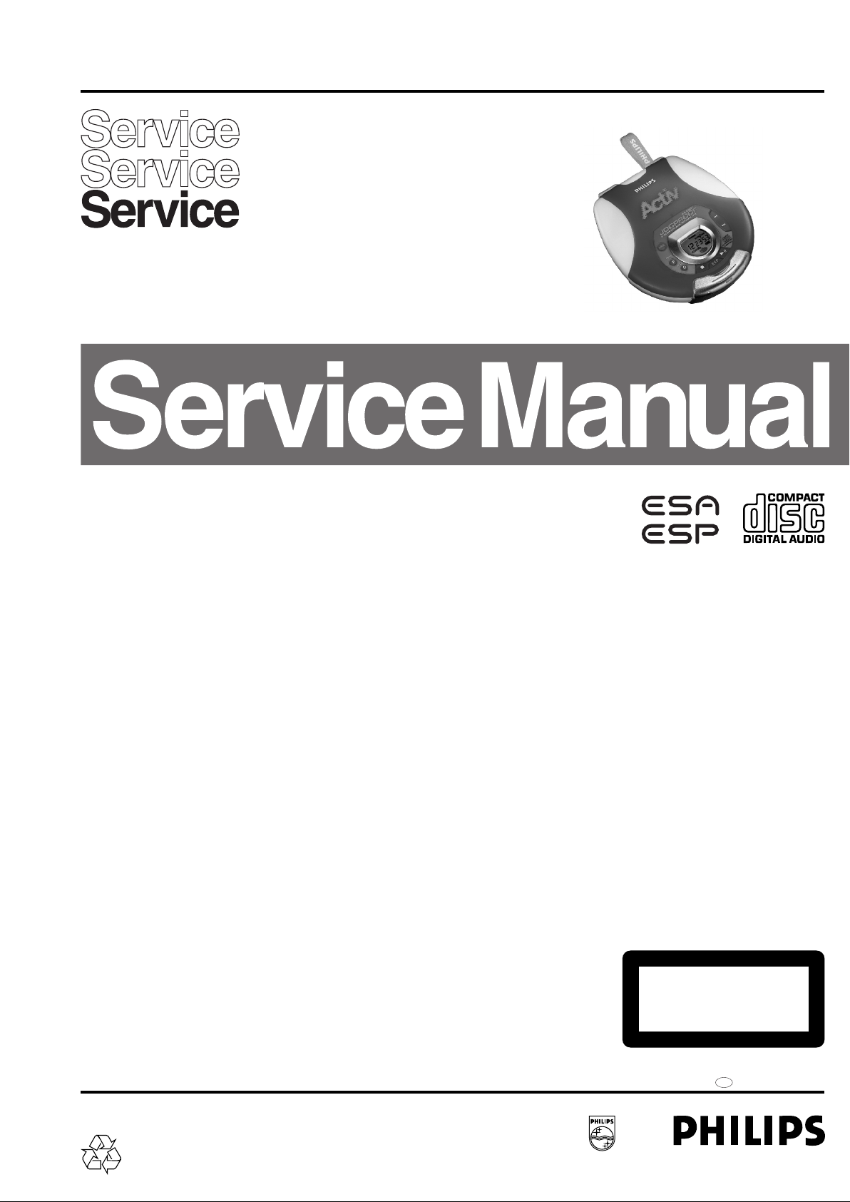
Portable Compact Disc Player
ACT7585
all versions
TABLE OF CONTENTS
chapter
Handling chip components and safety 1 - 1
Technical Specification 2 - 1
Measurement Setup
Connections & Controls
Instructions for use
Accessories 2 - 9
Features Overview
Service Tools 2 - 9
Training Material
.................................................................
................................................................
.................................................
......................................................
................................................
.................................................
.......................................................
...........................................................
.............................................
Service Test Program 3 - 1
Flow Chart
Block Diagram 3 - 3
Startup Procedure
Pinning of Intergated Circuits
...................................................................
....................................................
..............................................................
........................................................
.............................
...................................
2 - 1
2 - 2
2 - 3 to 2 - 8
2 - 9
2 - 9
2 - 9ESD Protection Equipment
3 - 2
3 - 4
3 - 5 to 3 - 7
CIRCUIT DIAGRAMS
Control/Supply part
Audio part
...................................................................
CD part
Membrane Assembly
LAYOUT DIAGRAMS
Component Side View
Copper Side View
Exploded View Diagram
Mechanical partslist
Electrical partslist
.......................................................
..................................................
.................................................
...............................................
..............................................
....................................................
..................................................
6 - 1 to 6 - 3
chapter
4 - 1
4 - 2...............................................................
4 - 3
4 - 6
4 - 4
4 - 5
5 - 1
4 - 6
Safety regulations require that the set be restored to its original
condition and that parts which are identical with those specified
be used.
C
Copyright 1995 Philips Consumer Electroncis B.V. Eindhoven, The Netherlands
All rights reserved. No part of this publication may be reproduced, stored in a retrieval
system or transmitted, in any form or by any means, electronic, mechanical, photocopying,
or otherwise without the prior permission of Philips.
Printed in The Netherlands Copyright reserved Subject to modification
PCS 107 221
CLASS 1
LASER PRODUCT
GB
3140 785 22590Published by SS 0109 Service Audio
Page 2
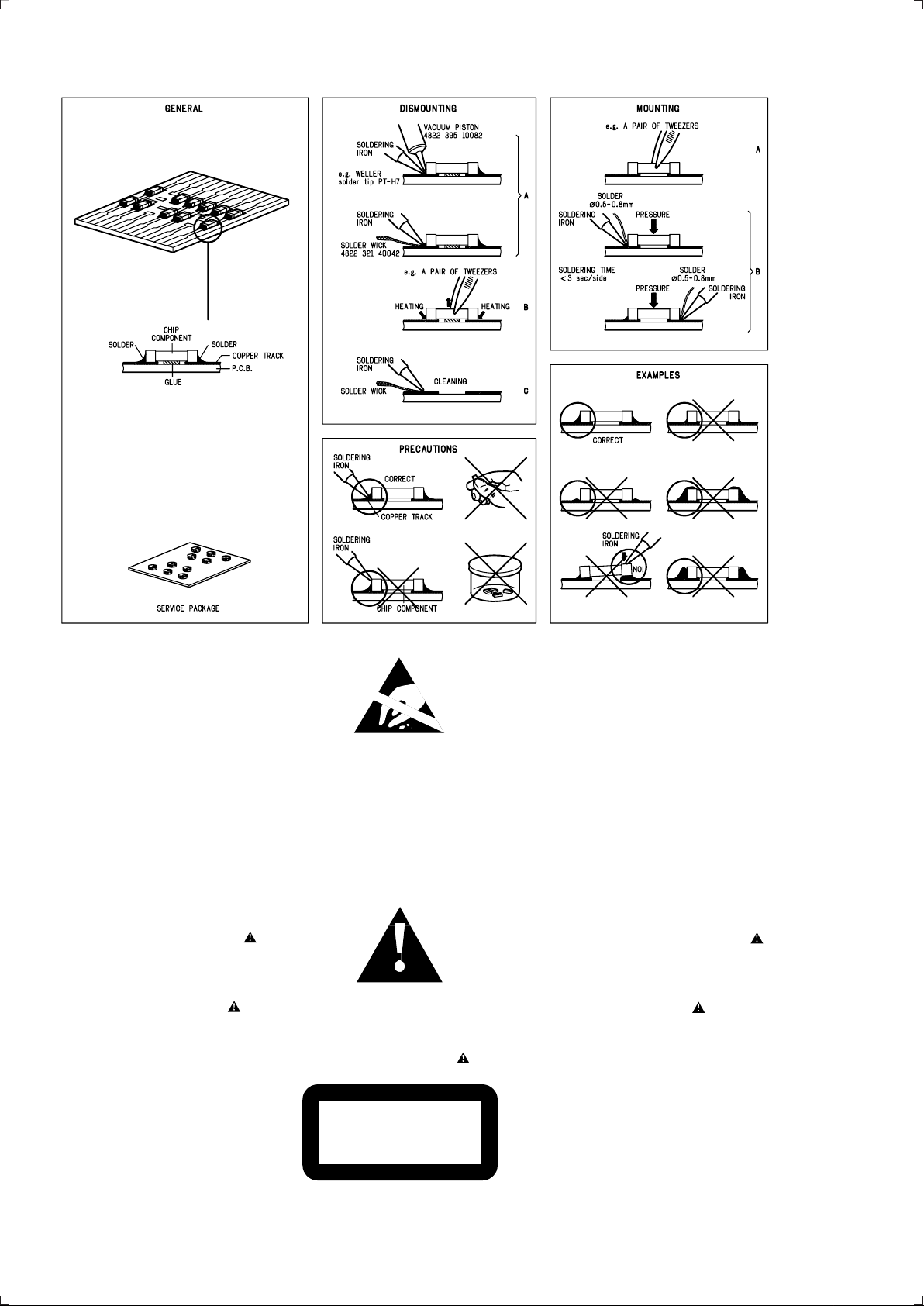
HANDLING CHIP COMPONENTS
1-1
© WARNING
All ICs and many other semiconductors are susceptible to
electrostatic discharges (ESD). Careless handling during
repair can reduce life drastically.
When repairing, make sure that you are connected with the
same potential as the mass of the set via a wristband with
resistance. Keep components and tools at this potential.
f ATTENTION
Tous les IC et beaucoup d ´autres semi-conducteurs sont
sensibles aux d écharges statiques (ESD). Leur long évite
pourrait être consid érablement écourt ée par le fait qu ´aucune
précaution n ést prise à leur manipulation.
Lors de r éparations, s ´assurer de bien être reli é au m ême
potentiel que la masse de l ´appareil et enfileer le bracelet
serti d ´une r ésistance de s écurit é.
Veiller à ce que les composants ainsi que les outils que l ´on
utilise soient également à ce potentiel.
©
Safety regulations require that the set be restored to its
original condition and that parts which are identical with
those specified be used.
Safety components are marked by the symbol
f
Les normes de s écurit é exigent que l`appareil soit remis
à l`état d`origine et que soient utilis ées les pi èces de
rechange identiques à celles sp écifiées.
Les composants de s écurit é sont marqu és
d WARNUNG
Alle ICs und viele andere Halbleiter sind empfindlich
gegen über elektrostatischen Entladungen (ESD).
Unsorgf ältige Behandlung im Reparaturfall kann die
Lebensdauer drastisch reduzieren.
Sorgen Sie daf ür, daß Sie im Reparaturfall über ein Pulsarmband mit Widerstand mit dem Massepotential des
Gerätes verbunden sind.
Halten Sie Bauteile und Hilfsmittel ebenfalls auf diesem
Potential.
d
Bei jeder Reparatur sind die geltenden Sicherheitsvorschriften zu beachten. Der Originalzustand des Ger ätes
darf nicht ver ändert werden. F ür Reparaturen sind Originalersatzteile zu verwenden.
Sicherheitsbauteile sind durch das Symbol markiert.
ESD
SAFETY
ñ WAARSCHUWING
Alle IC ´s en vele andere halfgeleiders zijn gevoelig voor
electrostatische ontladingen (ESD).
Onzorgvuldig behandelen tijdens reparatie kan de levensduur
drastisch doen vermindern. Zorg ervoor dat u tijdens reparat ie
via een polsband met weerstand verbonden bent met hetzelfde
potentiaal als de massa van het apparaat.
Houd componenten en hulpmiddelen ook op ditzelfde potentiaal .
i AVVERTIMENTO
Tutti IC e parecchi semi-conduttori sono sensibili alle scar iche
statiche (ESD).
La loro longevit à potrebbe essere fortemente ridatta in caso di
non osservazione della pi ù grande cauzione alla loro
manipolazione. Durante le riparationi occorre quindi essere
collegato allo stesso potenziale che quello della massa
delápparecchio tramite un braccialetto a resistenza.
Assicurarsi che i componenti e anche gli utensili con quali si
lavora siano anche a questo potenziale.
ñ
Veiligheidsbepalingen vereisen, dat het apparaat in zijn
oorspronkeliijke toestand wordt teruggebracht en dat
onderdelen, identiek aan de gespecificeerde, worden toegepas t.
De Veiligheidsonderdelen zijn aangeduid met het symbool
i
Le norme di sicurezza estigono che l ´apparecchio venga
rimesso nelle condizioni originali e che siano utilizzati i
pezzi di ricambiago identici a quelli specificati.
Componenty di sicurezza sono marcati con
©
DANGER : Invisible laser radiation when open.
AVOID DIRECT EXPOSURE TO BEAM.
s Varning !
Osynlig laserstr ålning n är apparaten är öppnad och
spärren är urkopplad. Betrakta ej str ålen.
∂ Advarsel !
Usynlig laserstr åling ved åbning n år sikkerhedsafbrydere
er ude af funktion. Undg å udsaettelse for str åling.
PCS 104 437
CLASS 1
LASER PRODUCT
ß Varoitus !
Avatussa laitteessa ja suojalukituksen ohitettaessa olet alt tiina
näkymättömälle laseris äteilylle. Älä katso s äteeseen !
©
After servicing and before returning the set to customer
perform a leakage current measurement test from all
exposed metal parts to earth ground, to assure no
shock hazard exists.
The leakage current must not exceed 0.5mA.
f
"Pour votre s écurite, ces documents doivent être utilis és par
des sp écialistes agr éés, seuls habilit és à réparer votre
appareil en panne".
Page 3
TECHNICAL SPECIFICATIONS
2-1
General
Dimension (W x H x D) : 133 x 32 x 148 mm
Weight : 225 g
Power supply modes
DC in socket : 4.5 – 5.5 V
Primary batteries : 1.75 – 3.6 V
Rechargable batteries : 1.75 – 3.6 V
Battery lifetime
Battery Type ESP OFF PSM ON ESP ON
Primary batteries 20 hrs typ. - 20 hrs typ.
Rech. batt. AY3362 9.5 hrs typ. - 9.5 hrs typ.
Battery level detection
Battery level 3 &empty : 0.7 V nom. ±100 mV
Battery level 2 &empty : 0.5 V nom. ±100 mV
Battery level 1 &empty : 0.3 V nom. ±100 mV
Battery empty : 1.8 V nom +100/-50 mV
Shock resistance (ESP off)
+X/-X direction : 2.5 G
+Y/-Y direction : 2.5 G
+Z/-Z direction : 2 G
Shock resistance with car base (ESP off)
+X/-X direction : 10 G
+Y/-Y direction : 10 G
+Z/-Z direction : 10 G
Headphone output (16 Ohm, ESP and DBB off)
Output power (10% THD) : 6 mW (+1/-3 dB)
Output power (10% THD) -/17 : 12 mW (+1/-3 dB)
Frequency response (1mW) : 100 Hz – 20kHz within 6 dB
S/N ratio (unw.) : 80 dB (83 dB typ.)
S/N ratio (A-wght) : 82 dB (85 dB typ.)
THD+N (1kHz, 1mW) : 1 % (0.2 % typ.)
Crosstalk (1kHz, w/o load) : -24 dB (-44 dB typ.)
Channel unbalance (-40dB) : 5 dB
Volume attenuation (1kHz) : > 60 dB
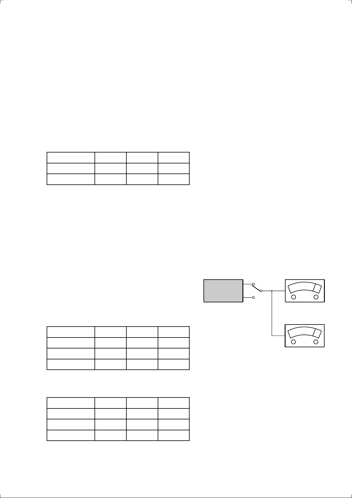
Measurement setup
Charge section
Charge current : 250 mA nom. ±10 %
Charge time for 80% AY3362 : 4.0 hrs nom.
Charge time for 100% AY3362 : 6.0 hrs nom.
Charge time limit : 7.0 hrs nom.
Temperature protection : 50 °C ± 5 °C
Current consumption DC–in supply (4.5 V)
Operation ESP OFF PSM ON ESP ON
Play mode 100 mA typ. - 100 mA typ.
Jump mode 220 mA typ. - 220 mA typ.
Standby 30 mA typ. - 30 mA typ.
Current consumption Battery supply (2.25 V)
Operation ESA OFF PSM ON ESA ON
Play mode 120 mA typ. - 120 mA typ.
Use Audio Signal Disc SBC429 4822 397 30184
(replaces test disc 3)
DUT
L
R
S/N and distortion meter
e.g. Sound Technology ST1700B
LEVEL METER
e.g. Sennheiser UPM550
with FF-filter
Jump mode 400 mA typ. - 400 mA typ.
Standby 0.05 mA typ. - 0.05 mA typ.
PCS 107 222
Page 4
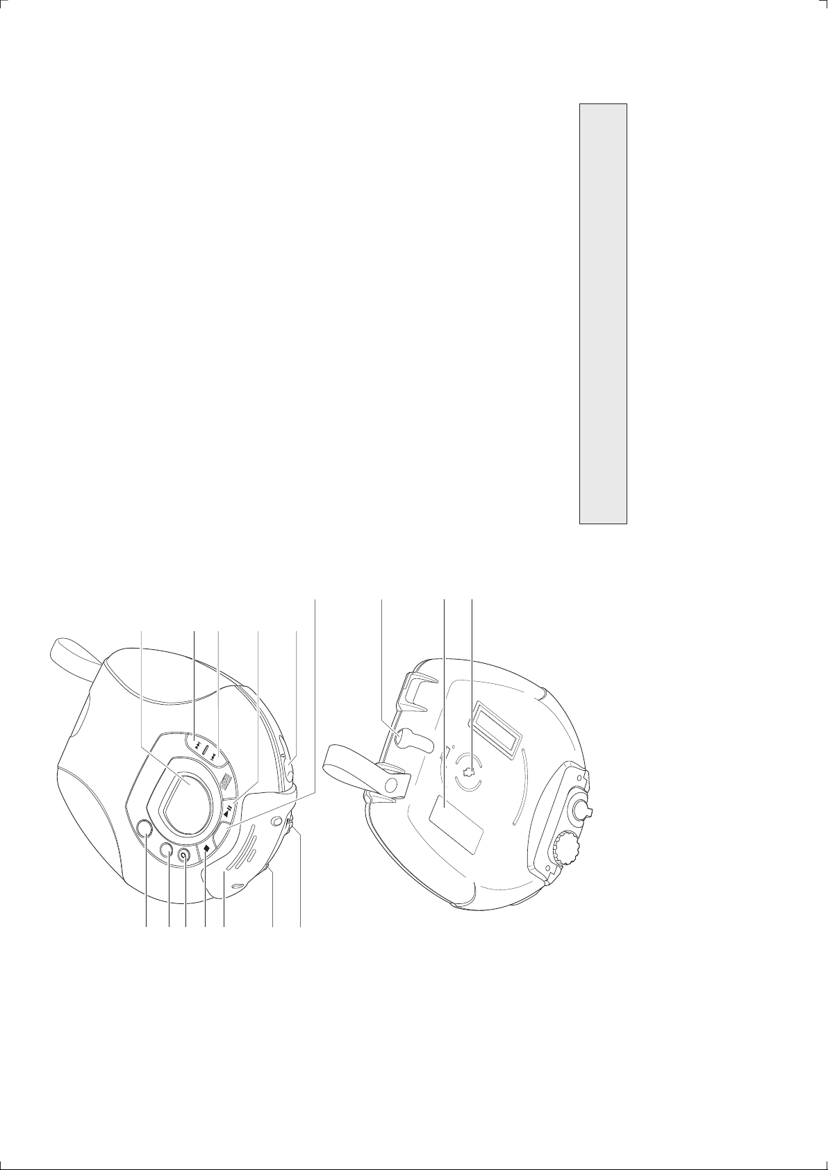
CONNECTIONS AND CONTROLS
on and off This button also switches acoustic feedback (the beep)
on/off when it is pressed for more than 2 seconds
SHUFFLE REPEAT ALL, REPEAT, REPEAT ALL and SCAN
2-2
.
opean Community
Eur
the set off
regardless of vibrations and shocks
1 p /LINE OUT.3.5mm headphone socket
2 2;.................switches the set on, starts and interrupts CD play
HOLD............locks all buttons
OFF.................switches RESUME and HOLD off
3 ∞..................skips and searches backward
4 §..................skips and searches forward
5 .......................display
6 DBB................DIGITAL DYNAMIC BASS BOOST: switches the bass enhancement
5
DBB
PROG
7 PROG P..........programs tracks and reviews the program
8 MODE............selects the different playing possibilities: SHUFFLE,
9 9....................stops CD play, erases a program, activates charging and switches
0 .......................open the CD lid here
! RESUME........stores the last position played
#
3
4
P
MODE
ESP
2
1
/ LINE OUT
VOL
@ VOL E.......adjusts the volume
# ESP ................ELECTRONIC SKIP PROTECTION ensures continuous CD playback
$
$ 4.5V DC..........socket for external power supply
%
% ........................typeplate
^ ........................belt clip holder
^
This set complies with the radio interference requirements of the
PCS 107 223
76890
!
@
Page 5
INSTRUCTIONS FOR USE
2-3
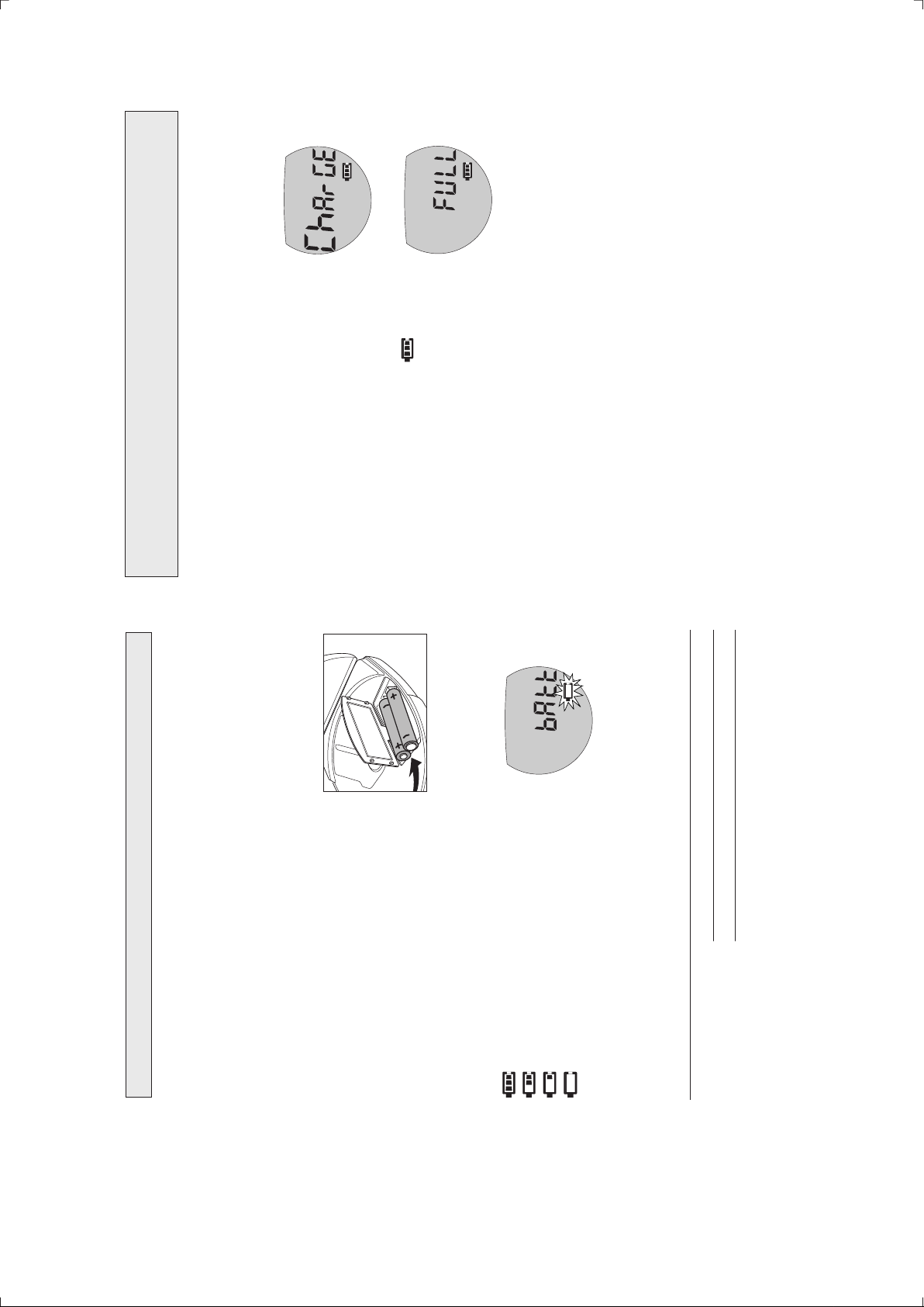
echargeable ECO-PLUS NiMH battery
ECO-PLUS NiMH battery information (for versions supplied with
the rechargeable ECO-PLUS NiMH battery AY 3362)
Recharging works only on players supplied with the rechargeable ECO-PLUS NiMH
battery AY 3362.
during recharging.
approximately 30 minutes and Hot is displayed.
– If the batteries become too warm, recharging will be interrupted for
– To ensure proper recharging on board, take care that contacts are clean.
seconds.
the player and then to the wall socket.
y A is shown and ChArGEis displayed for 5
Recharging the ECO-PLUS NiMH battery on board
1 Insert the rechargeable ECO-PLUS NiMH battery AY 3362.
2 Connect the mains adapter to the 4.5V DC socket of
when you start playback.
• Recharging stops after a maximum of 7 hours, or
3 When the battery is fully recharged, and
FULL appear briefly in the display, before the
display switches off.
Notes: – It is normal for the batteries to become warm
– Use only the ECO-PLUS NiMH battery AY 3362.
Handling instructions
• Recharging already charged or half-charged batteries will shorten their lifetime.
We therefore recommend that you let the r
run till it is completely empty before you recharge it.
• To avoid a short circuit, do not let the battery touch any metal object.
If the battery becomes empty soon after recharging, then either its contacts are
•
dirty or it has reached the end of its lifetime.
(supplied or optionally available)
Batteries
You can use the following batteries with this CD-player:
• normal batteries type LR6, UM3 or AA (preferably Philips), or
• alkaline batteries type LR6, UM3 or AA (preferably Philips).
Note: – Old and new or different types of batteries should not be used in
combination. Remove batteries if they are empty or if the player is
not going to be used for a long time.
Inserting batteries
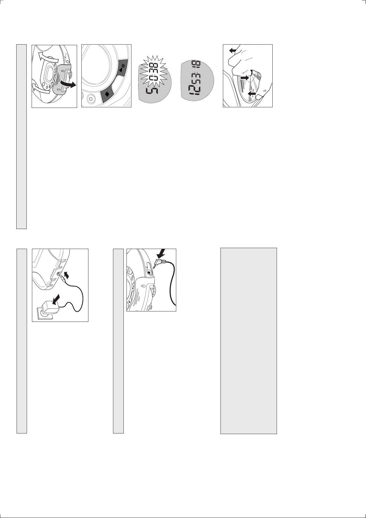
1 Unfasten the buckle.
2 Open the CD lid.
2 alkaline batteries, or the rechargeable NiMH
3 Open the battery compartment and insert either
battery AY 3362 (if supplied).
Batteries contain chemical substances, so they
should be disposed of properly.
Battery full
Battery indication
The approximate power level of your batteries is shown in the display.
Battery two-thirds full
Battery one-third full
Battery dead or empty. When the batteries are
dead or empty, the symbol A flashes,
bAtt is displayed, and the beep tone sounds repeatedly.
Average playing time of batteries under normal conditions
Battery type ESP on ESP off
Normal 7 hours 6 hours
Alkaline 22 hours 19 hours
Rechargeable ECO-PLUS NiMH battery 10 hours 9 hours
PCS 107 224
Page 6
INSTRUCTIONS FOR USE
ESP
/ LINE OUT
VOL
RESUME
HOLD
0
MODE
ESP
PROG
MODE
DBB
ESP
P
/ LINE OUT
VOL
OFF
RESUME
HOLD
2-4
ess the
Playing a CD
This CD-player can play all kinds of Audio Discs such
time are displayed.
CD onto the hub.
as CD-Recordables and CD-Rewritables. Do not try to
play a CD-ROM, CDi, VCD, DVD or computer CD.
1 Unfasten the buckle.
2 Open the CD lid.
3 Insert an audio CD, printed side up, by pressing the
4 Close the lid by pressing it down on the left side.
y The current track number and elapsed playing
5 Press 2; to switch the player on and start playback.
flashing.
y The time at which playback was paused starts
• You can pause playback by pressing 2;.
• You can continue playback by pressing 2; again.
time of the CD are displayed.
y The total number of tracks and the total playing
6 Press 9 to stop playback.
switch off after a while to save energy.
hub gently while lifting the CD.
7 Press 9 again to switch the player off.
• To remove the CD, hold it by its edge and pr
Note: If there is no activity, the set will automatically
e an open-air type
ound you.
PCS 107 225
Mains adapter (supplied or optionally available)
Use only the AY 3170 adapter (4.5 V/300 mA direct
current, positive pole to the centre pin). Any other
player to your HiFi system (with a signal lead) or to
your car radio (with a cassette adapter or signal
lead). In both cases, the volume of the player must
be set to position 8.
corresponds to the local voltage.
the player and to the wall socket.
product may damage the player.
1 Make sure that the adapter’s voltage
2 Connect the adapter to the 4.5V DC socket of
Note: Always disconnect the adapter when you are not using it.
Headphones AY 3678
• Connect the supplied headphones to the p/LINE OUT
socket of the player.
Note: p/LINE OUT can also be used for connecting the
Use your head when using headphones
Hearing safety: Do not play your headphones at a high volume. Hearing experts
advise that continuous use at high volume can permanently damage your hearing.
Traffic safety: Do not use headphones while driving a vehicle. It may create a hazard
and it is illegal in many countries. Even if your headphones ar
designed to let you hear outside sounds, do not turn up the volume so high that you
cannot hear what is going on ar
Page 7
INSTRUCTIONS FOR USE
DBB
PROG
MODE
DBB
P
VOL
OFF
RESUME
HOLD
2-5
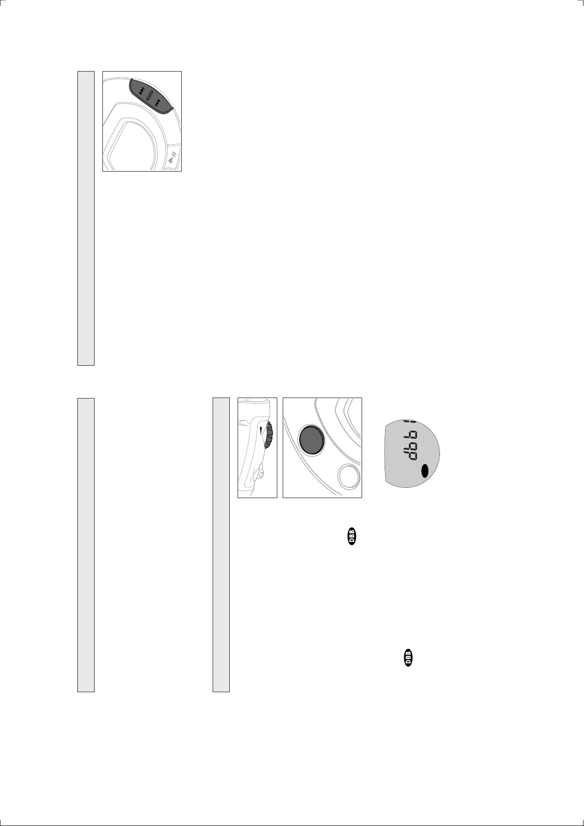
Selecting a track and searching
Selecting a track during playback
while playing a program, searching is only possible within the particular
track.
the track’s number is displayed.
y Playback continues with the selected track, and
Briefly press ∞ or § once or several times to skip to
the current, previous or next track.
Selecting a track when playback is stopped
1 Briefly press ∞ or § once or several times to select
the desired track. The track number is displayed.
2 Press 2; to start CDplay.
y Playback starts with the selected track.
Searching for a passage during playback
1 Keep ∞ or § pressed to find a particular passage in
a backward or forward direction.
y Searching starts while playback continues at low
volume. After 2 seconds the search speeds up.
y Playback continues from this position.
2 Release the button when you reach the desired passage.
– In SHUFFLE, SHUFFLE REPEATALL or REPEAT mode (see MODE chapter), or
Notes: – If the player is in SCAN mode (see MODE chapter), searching is not possible.
f, press BASS
dbb1 and twice
Playback information
• If a CD-Recordable (CD-R) or a CD-Rewritable (CD-RW) is not recorded properly,
nF dISC is displayed, indicating that the CD has not been finalized. In that
case, use FINALIZE on your CD recorder to complete the recording.
after pressing 2; for sound reproduction to start.
• When playing a CD-Rewritable (CD-RW), please note that it takes 3–15 seconds
• Playback will stop if you open the CD lid.
dbb1 or dbb2 of
is shown.
ess BASS once for
for dbb2.
• While the CD is read, 1 -:- flashes in the display.
Volume and bass
Volume adjustment
• Adjust the volume by using VOL E.
Bass adjustment
You can choose between the bass enhancement levels
dbb1 and dbb2.
y dbb1 or dbb2is displayed and
1 Pr
o switch
twice or once, respectively.
2 T
y goes off.
PCS 107 226
Page 8
INSTRUCTIONS FOR USE
PROG
MODE
DBB
P
MODE
P
2-6
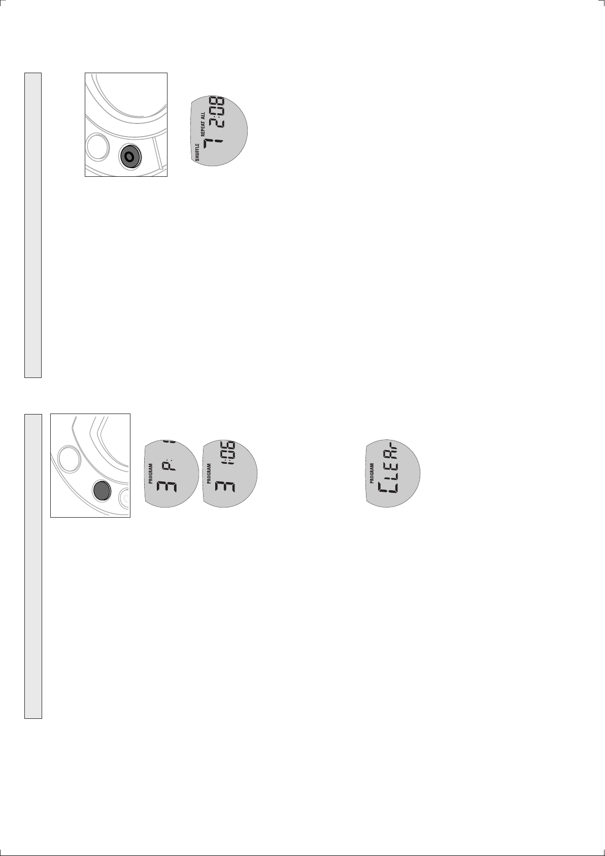
Selecting different playing possibilities – MODE
It is possible to play tracks in random order, to repeat a single track or the entire CD,
and to play the first few seconds of each track.
random order until all of them have been played
once.
played repeatedly in random order.
order to activate one of the following ‘modes’. The
active mode is shown in the display.
y SHUFFLE: All tracks of the CD are played in
y SHUFFLE REPEAT ALL: All tracks of the CD are
y REPEAT: The current track is played repeatedly.
1 Press MODE during playback as often as required in
y REPEAT ALL: The entire CD is played repeatedly.
remaining tracks are played in sequence.
y SCAN: The first 10 seconds of each of the
2 Playback starts in the chosen mode after 2 seconds.
until the display shows no active modes.
• To return to normal playback, press MODE repeatedly
e displayed.
Programming track numbers
PCS 107 227
You can store up to 30 tracks to play in a program.
A single track may be stored more than once in the
program.
1 While playback is stopped, select a track with
SELECt is displayed.
programmed and P with the total number of
stored tracks ar
∞ or §.
2 Press PROG P to store the track.
y PROGRAM lights up; the track number
y PROGRAM is shown and playback starts.
3 Select and store all desired tracks in this way.
4 Press 2; to start playback of your selected tracks.
• You can review the program by pressing PROG P for
y The display shows all the stored tracks in sequence.
more than 2 seconds.
– If you try to store more than 30 tracks, FULL is displayed.
Notes: – If you press PROG P and there is no track selected,
Clearing the program
• While playback is stopped, press 9 to clear program.
and the program is cleared.
y CLEAr is displayed once, PROGRAM goes off,
supply is interrupted, or if the CD-player lid is opened, or if the set switches
off automatically.
Note: The program will also be cleared if the power
Page 9
INSTRUCTIONS FOR USE
HOLD
VOL
OFF
RESUME
HOLD
ESP
ESP
2-7
ESP
Conventional portable CD-players subjected to a shock
or vibration during playback often skip parts of the CD. The
ELECTRONIC SKIP PROTECTION (ESP) feature, with which
your set is equipped, however, prevents such loss of
continuity when your player is subjected to light vibrations.
But ESP does not prevent playback interruptions caused by
vigorous exercise. Nor does it protect against damage
resulting from the player being dropped!
• Press ESP during playback to activate the skip
protection.
y ESP is shown and the protection is activated.
y ESP goes off and the protection is deactivated.
• To deactivate the skip protection, press ESP again.
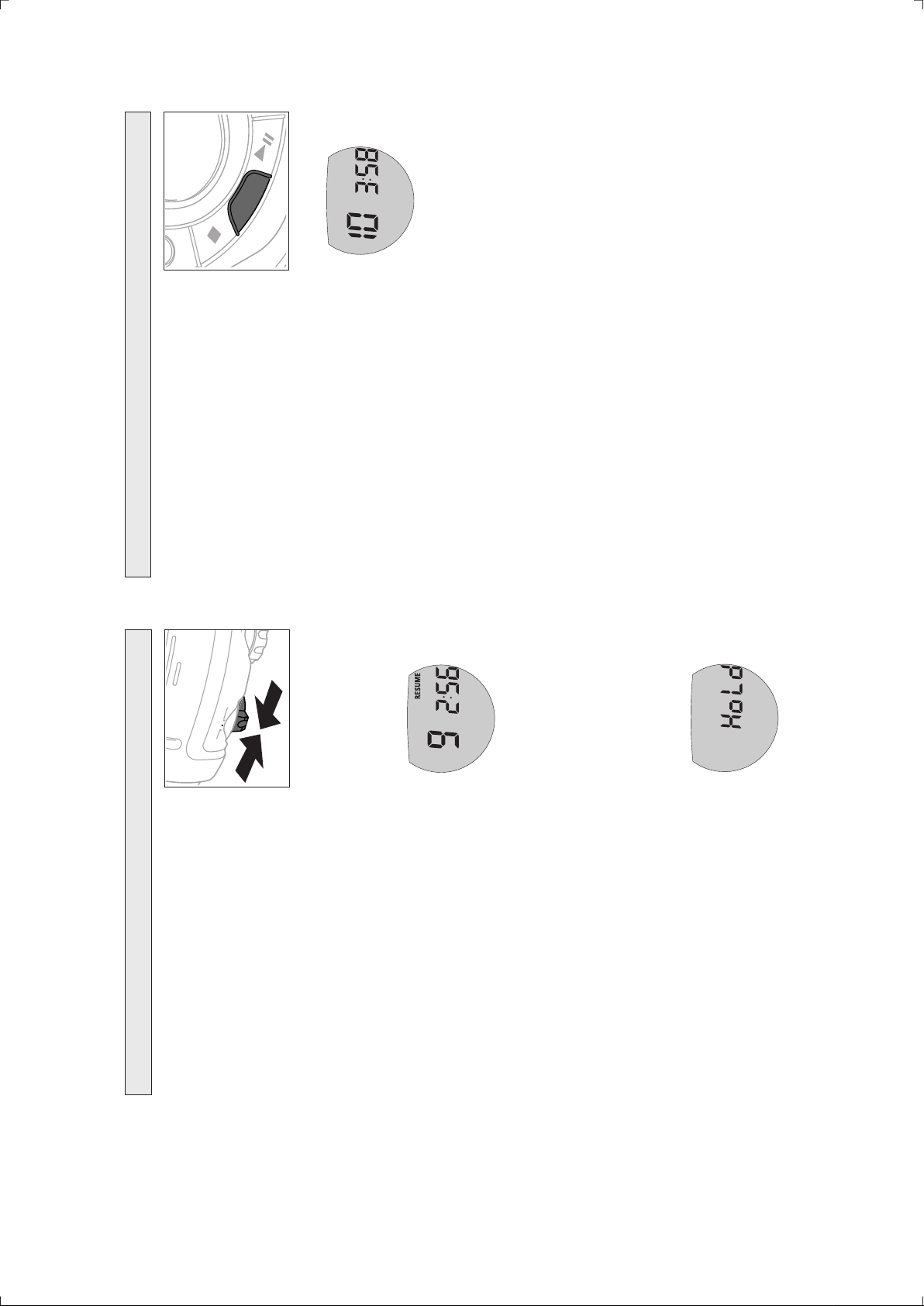
ess any button. If the set is
HOLD is shown when you pr
e locked.
RESUME and HOLD
You can interrupt playback and continue (even after an
extended period of time) from the position where
playback stopped (RESUME) and you can lock all buttons
of the set so that no action will be executed (HOLD).
Use the RESUME–HOLD–OFF slider for these functions.
RESUME – continuing from where you have
stopped
1 Switch the slider to RESUME during playback to activate RESUME.
y RESUME is shown.
2 Press 9 whenever you want to stop playback.
3 Press 2; whenever you want to resume playback.
y RESUME is shown and playback continues from
where you have stopped.
switched off, HOLD will be shown only when 2; is pressed.
y RESUME goes off.
• To deactivate RESUME, switch the slider to OFF.
HOLD – locking all buttons
You can lock the buttons of the set by switching the slider to HOLD. Now, when a key
is pressed, no action will be executed. This is of use, for example, when transporting
the player in a bag. With HOLD activated, you can avoid accidental activation of other
functions.
1 Switch the slider to HOLD to activate HOLD.
y All buttons ar
2 To deactivate HOLD, switch the slider to OFF.
RESUME, you will be activating the RESUME
Note: If you deactivate HOLD by switching the slider to
function.
PCS 107 228
Page 10
INSTRUCTIONS FOR USE
RESUME, SHUFFLE or PROGRAM is Switch RESUME, SHUFFLE
active. or PROGRAM off.
Check and clean
Loose, wrong or dirty
connections connections.
Volume is not adjusted. Adjust the volume.
Malfunctions due to nearness Keep the player away from
of active mobile phones active mobile phones.
Strong magnetic fields near Change the player’s position
2-8
unsafe operation.
the player or connections.
In-car use
cassette adapter is Insert the cassette adapter
inserted incorrectly. correctly.
Temperature inside the car Let the player adjust to the
is too high/low. temperature.
Cigarette lighter socket Clean the cigarette
is dirty. lighter socket.
Wrong playback direction of the Change the autoreverse
car cassette player’s direction.
autoreverse feature
If a fault occurs, first check the points listed, before taking the set for repair.
If you are unable to solve a problem by following these hints, consult your dealer or
service centre.
Problem Possible cause Solution
The CD skips tracks. The CD is damaged or dirty. Replace or clean the CD.
ectly Insert the batteries
No sound or PAUSE is activated. Press 2;.
bad sound quality
Batteries are empty. Change the batteries.
Contact pins are dirty. Clean them with a cloth.
Mains adapter
Loose connection Connect the adapter
securely.
will invalidate the guarantee.
In-car use
Cigarette lighter is not powered Switch on ignition or insert
when ignition is off. batteries.
the recording.
CD is not or incorrectly inserted. Insert a CD, label upwards.
The laser lens is steamed up. Wait until the lens has
cleared.
power supply or take out
ge Disconnect the set from
Electrostatic dischar
the batteries for
a few seconds.
CAUTION
Use of controls or adjustments or performance of procedures other
than herein may result in hazardous radiation exposure or other
WARNING
PCS 107 229
Under no circumstances should you try to repair the set yourself as this
Problem Possible cause Solution
No power, Batteries
playback does Batteries inserted incorr
not start correctly.
nF dISC CD-RW (CD-R) is not recorded Use FINALIZE on the
indication properly. CD recorder to complete
no dISC The CD is badly Replace or clean the CD.
indication scratched or dirty.
HOLD indication HOLD is activated. Deactivate HOLD.
and/or no reaction
to controls
Page 11
2-9
ACCESSORIES
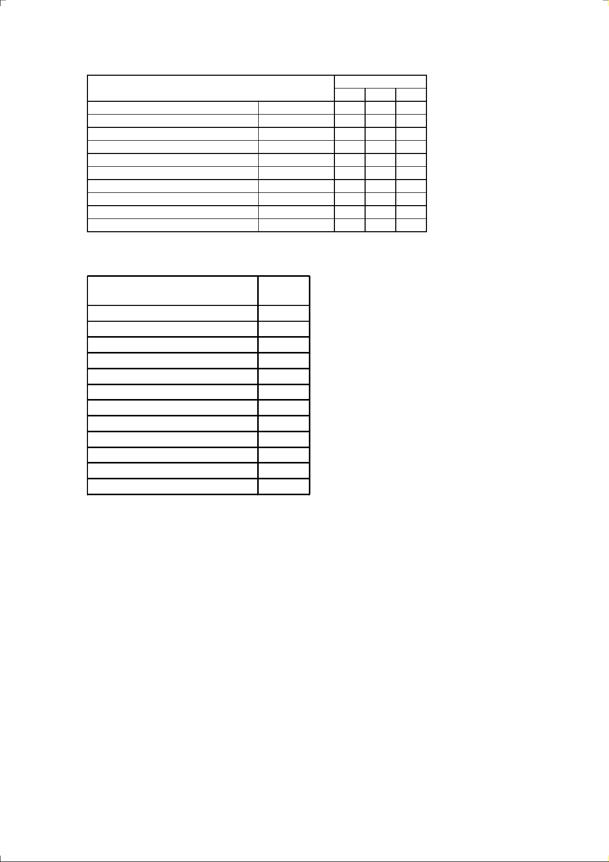
ACCESSORIES FOR CD-PORTABLE ACT7585
/00 /01 /17
AY3170/00 AC/DC ADAPTOR 482221910617 X
AY3160/02 AC/DC ADAPTOR 482221910449 X
AY3170/17 AC/DC ADAPTOR 482221910616 X
AY3266 POUCH 314011310360 X X X
AY3362 BATTERY NIMH-R6 310330884120 X X X
AY3501/00 CAR ADAPTOR CASSETTE 482239710059 O O O
AY3545/00 CAR DC/DC CONVECTER 482221910033 O O O
AY3678V/00 HEADPHONE 482224211007 X X X
AY3860/00 ACTIVE SPEAKER BOX 482244510513 O O O X - SUPPLY WITH THE SET
AY3464 HIFI CORD 482232011881 O O O O - OPTIONAL AVAILABLE
FEATURES OVERVIEW
FEATURES OF CD-PORTABLE
ELECTRONIC SKIP PROTECTION (ESP) 43.2 sec.
CD REWRITABLE COMPATIBLE X
POWER SAVE MODE (ESP) HOLD / RESUME FUNCTION X / X
DBB STAGES 2
ACOUSTIC FEEDBACK X
PROGRAM MEMORY 30
RECHARGE FUNCTION NiCd / NiMH - / X
EXTERNAL BATTERY BOX PREPARED LCD ILLUMINATION CORD REMOTE CONTROL PREPARED LINE / DIGITAL OUTPUT - / -
ACT7585
all versions
SERVICE TOOLS
Audio signal disc SBC429 4822 397 30184
Playability test disc SBC444 4822 397 30245
Test disc 5 (disc without errors) + Test disc 5A (disc with dropout errors,
Black spots and fingerprints) SBC426/SBC426A 4822 397 30096
TRAINING MATERIAL
Portable CD 1994 – Principles of Electronic Shock Absorption System ESA,
Portable CD 1996 – Key components 1996, Battery charging, DC/DC-converter 4822 725 24986
Protable CD 1998 – Key components 1998, Power Save Mode PSM 4822 725 26017
Key components 1994, Remote control system 4822 725 24941
(available from April 1998 onwards)
ESD PROTECTION EQUIPMENT
Anti-static table mat large 1200x650x1.25mm 4822 466 10953
Anti-static wristband 4822 395 10223
Connection box (3 press stud connections, 1M
Extendible cable (2m, 2MW , to connect wristband to connection box) 4822 320 11305
Connecting cable (3m, 2M
Earth cable (1M
KIT ESD3 (combining all 6 prior products – small table mat) 4822 310 10671
Wristband tester 4822 344 13999
small 600x650x1.25mm 4822 466 10958
W ) 4822 320 11307
W , to connect table mat to connection box) 4822 320 11306
W , to connect any product to mat or to connection box) 4822 320 11308
PCS 107 230
Page 12

SERVICE TEST PROGRAM
3-1
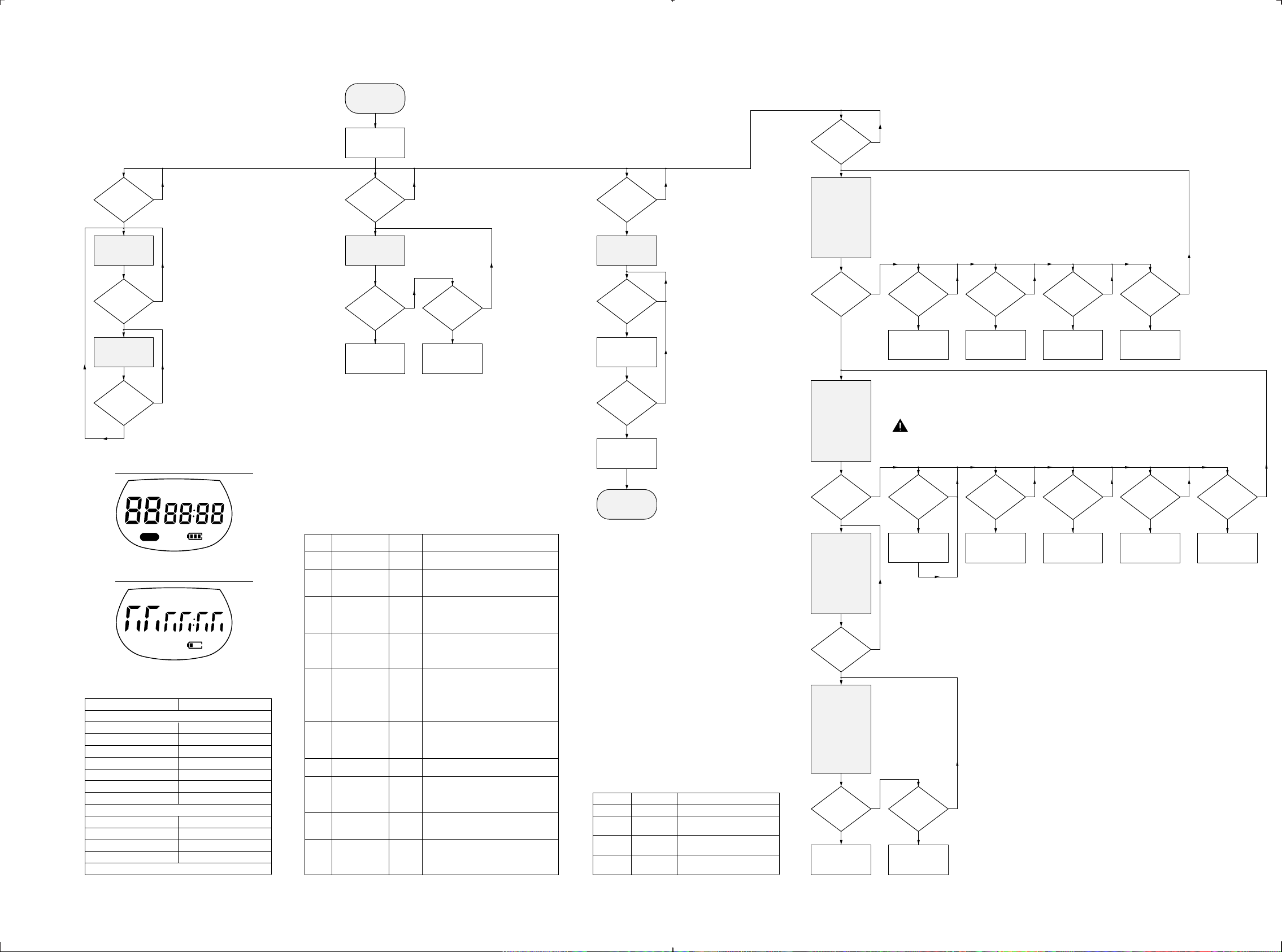
1. PRELIMINARY SETUP
• To enter the service test program disconnect the AC/DC adaptor
and remove batteries, open the CD-door and hold the buttons
“PLAY” & “PREV” depressed while turning power on (i.e.
connecting the AC/DC adaptor).
• The display shows the software version of the built-in µP
(i.e. “S-26”). Versions are counted from “00” onwards; that
means the higher the number the newer the software.
• The program is now in the main menu – various tests can be
entered by pressing the corresponding buttons (see flow chart on
next page or detailed description of available tests below).
• To exit the service test program press the “STOP“ button or
disconnect the set from the power source.
2. DISPLAY TEST
Purpose: Check functionality of display and display driver.
• To enter the display test start the service test program and press
the “NEXT” button.
• The display shows test pattern1. All segments are activated for
finding open circuits (see flow chart on next page).
• To jump to the next pattern press the “NEXT” button.
• The display shows test pattern2. All alternate pins (2, 4, ...) are
activated for finding short circuits (see flow chart on next page).
• To jump back to test pattern1 press the “NEXT” button, to exit the
display test and return to the main menu press the “STOP” button.
3. KEY TEST
Purpose: Check operation of keys and cord remote control.
• To enter the key test start the service test program and press the
“MODE” button.
• The display shows “--”.
• Hold key depressed and check corresponding key code on the
display. Key codes can be found in table1 (see flow chart on next
page).
• To exit the key test and return to the main menu press the “STOP”
button.
4. PLAYBACK TEST WITH ERROR ANALYSIS
Purpose: Analyze errors that occur during playback and search for
intermittent failures.
• To enter the playback test start the service test program and press
the “BASS” button.
• To start the error analysis press the “PLAY” button. Note that the
playback test can only be entered if the CD-door is closed.
• The set will read the TOC and start playback.
As long as the playback is free of errors the display shows track and
time information like in normal play-mode. In case of errors
corresponding error codes will be displayed. The meaning of these
error codes can be found in table2 (see flow chart on next page).
Note: Errors can either be
“fatal”
or
“non fatal”
. Fatal errors always
stop the playback, non fatal errors only cause a short
interruption of the music. Fatal errors are displayed as long
as the set is connected to the power source, non fatal errors
are displayed until a new error occurs or a button is pressed.
• To stop the playback test disconnect the set from the power
source.
5. SERVO TEST
Purpose:
Check door switch, inner switch of CD-drive, movement
of slide and acceleration of discmotor.
• To enter the servo test start the service test program and press
the “PLAY” button.
• The display shows “Cdxy”.
“x” indicates state of door switch;
“y” indicates state of inner switch.
x,y
= “0” means switch is closed; “1” means switch is open.
• To move slide outside hold the “NEXT” button depressed.
• To move slide inside hold the “PREV” button depressed.
• To accelerate the discmotor clockwise hold the “MODE” button
depressed.
• To accelerate the discmotor counter-clockwise hold the “PROG”
button depressed.
• To enter the focus test press the “PLAY” button, to exit the servo
test and return to the main menu press the “STOP” button.
6. FOCUS TEST
Purpose: Check movement of lens and operation of focus servo for
CDDA and CDRW discs.
Since the CDRW reflects much less light than an ordinary CDDA, the gain
of the HF-amplifier stage and the sensitivity of the ADC inside the
Decoder&Digital Servo IC “CD10” must be adapted accordingly.
The gain is switched via the CDRW input of the HF-preamplifier.
The ADC-sensitivity is set via software parameters (sent from µP to
“CD10”). In total, there are 4 sensitivity modes available: 1 for CDDA and
3 for CDRW. The modes are listed in table3 (see next page).
In normal play-mode, the correct focus sensitivity is choosen
automatically during start-up (see “Start-up procedure” on previous page).
In the service test program, the sensitivity can be choosen manually in
order to allow individual measurements in several modes.
• The focus servo loop is switched on and the set starts searching
the focus (“focus ramping”). As soon as the focus has been found
the focus servo loop is closed and the state of the focus is
monitored continuously.
• If the focus is OK the display shows “ Fx”, else “-Fx”.
“x” indicates the sensitivity mode. Details can be found in table3
(see flow chart on next page).
• To toggle between sensitivity modes press the “BASS” button.
• To move slide outside hold the “NEXT” button depressed.
• To move slide inside hold the “PREV” button depressed.
• To accelerate the discmotor clockwise hold the “MODE” button
depressed.
• To accelerate the discmotor counter-clockwise hold the “PROG”
button depressed.
• In case the focus is OK the discmotor test can be entered by
pressing the “PLAY” button, to exit the focus test and return to the
main menu press the “STOP” button.
7. DISCMOTOR TEST
Purpose: Check speed regulation of discmotor.
• The speed regulation is switched on and the discmotor starts
rotating. If the speed reaches 75% of the nom. speed the display
shows “ d”, else “-d”.
• In parallel also the state of the focus is monitored continuously
(display “ Fx” or “-Fx”).
• In case the disc speed is OK and the focus is OK the radial test
can be entered by pressing the “PLAY” button, to exit the
discmotor test and return to the main menu press the “STOP”
button.
8. RADIAL TEST
Purpose: Check if radial loop locks and an audio signal is audible
at the headphone output.
• The radial servo loop is switched on, mute is released and the
audio signal is audible. If the system is on track the display shows
“ r”, else “-r”.
• In parallel also the disc speed (display “ d” or “-d
”) and the state
of the focus (display “ Fx” or “-Fx”) are monitored continuously.
Note: In case of radial errors the audio output is muted and muting
is not released automatically when the systems recovers from the
error. “-r” remains on the display.
To open mute again press the “NEXT” or “PREV” button.
• To jump 16 tracks outside press the “NEXT” button.
• To jump 16 tracks inside press the “PREV” button.
• To exit the radial test and return to the main menu press the
“STOP” button, to exit the service test program disconnect the set
from the power source.
Important remark:
In radial test mode data to the DRAM is written at 1.2 times the
nominal speed, and read from the DRAM at nominal speed.
Because writing is done faster than reading the DRAM gets full after
a certain time.
In normal play mode the system would now wait until the DRAM is
partly emptied again, jump backwards and resume filling at the last
written position. However, in radial test mode the jumps would
disturb measurements on the radial servo loop.
Therefore this function has been disabled and filling restarts
immediately from the current position of the pick-up unit. As a result
“jumps” are audible during playback.
PCS 107 231
Page 13
SERVICE TSET PROGRAM
3-2 3-2
“NEXT”
pressed?
DISPLAY TEST 1
display shows
test pattern 1
“NEXT”
pressed?
DISPLAY TEST 2
display shows
test pattern 2
“NEXT”
pressed?
N
Y
N
Y
N
Y
test pattern1
REPEAT ALL
ESP
RESUMESHUFFLE
HOLD
PROGRAM
DBB
test pattern2
RESUME
table1 – key test
DISPLAY SET
KEYS OF SET
DBB
PROGRAM
MODE
PLAY
NEXT
PREVIOUS
ESP
1
2
3
5
6
7
8
KEYS OF CORD REMOTE CONTROL
STOP
PLAY
NEXT
PREVIOUS
4 rc
5 rc
6 rc
7 rc
Press “STOP” on the CD-player to exit the key test.
PRELIMINARY
SETUP
Display shows
software-v
ersion
26”)
(e.g. “S-
“MODE”
pressed?
Y
KEY TEST
Display shows
“--”
key on
cd-player
depressed?
YY
Display shows
keycode
(see table1)
table2 – playback error analysis
CODE
E 1000
E 1001
E 1002
E 1003
E 1004
E 1005
E 1006
E 1008
E 1009
E 1020
ERROR
focus error
radial error
sledge in error
sledge out error
DRAM filling
error
jump error
subcode error
turntable motor
error
audio error
(error flag)
focus search
error
TYPE
non fatal
non fatal
non fatal
non fatal
non fatal
non fatal
non fatal
fatal
non fatal
fatal
To enter the service test program
1. Disconnect the AC/DC adaptor and remove batteries
2. Open the CD-door
3. Hold “PLAY” & “PREV” buttons depressed
Connect the AC/DC adaptor or insert batteries
4.
MAIN MENU
N
on
N
key
remote control
depressed?
Display shows
keycode + “rc”
(see table1)
CAUSE
Focus point lost for at least 3ms.
The radial servo was offtrack for a
certain amount of time.
The slide did not reach it´s inner pos.
(inner switch of CD-drive does not close)
within approx. 6s.
The slide did not come out of it´s inner
pos. (inner switch of CD-drive is open)
within approx. 250ms.
The DRAM controller was not able to
connect two consecutive audio frames.
The microcontroller had to perform a
direct audio connection that produces
audible clicks.
The offtrack values do not decrease
properly when jumping tracks, the jump
destination could not be found.
No valid subcode for approx. 230ms.
During start-up, the disc speed did not
reach 75% of the nom. speed within
approx. 6 seconds.
Uncorrectable audio error (EF error flag
from CD-Decoder).
The focus point could not be found
within approx. 10s (no valid TOC info),
resp. 30s (valid TOC info).
Remark: Playback test can only
be entered if CD-door
is closed!
N
“DBB"
pressed?
PLAYBACK
TEST
Error during
playback?
Display shows
error-code
(see table2)
Fatal error?
N
Y
N
Y
N
Y
Stop playback
EXIT
SERVICE TEST
PROGRAM
table3 – focus sensitivity
DISPLAY
-F 01
-F 02
-F 03
-F 04
ESP-FLAG
off
on
on
on
FOCUS SENSITIVITY
Normal focus sensitivity for CDDA
Low focus sensitivity for
high-reflective CD-RW
Medium focus sensitivity for
normal-reflective CD-RW
High focus sensitivity for
low-reflective CD-RW
“PLAY”
pressed?
Y
SERVO TEST
Display shows:
xy”
“Cd
• State of switches
x = door switch
y = inner switch
“0” = closed
“1” = open
“PLAY”
pressed?
Y
FOCUS TEST
• Focus status
x” = focus OK
“ F
x” = focus error
“-F
x = focus sensitivity
(see table3)
Note: If focus has
been lost, focus
start-up procedure
is entered (ramping).
“PLAY”
pressed and
focus OK?
Y
DISC MOT. TEST
• Disc speed status
“ d” = speed OK
“-d” = speed error
• Focus status
” = focus OK
x
“ F
x” = focus error
“-F
x = focus sensitivity
(see table3)
“PLAY”
and focus OK
and speed
OK?
Y
RADIAL TEST
• On track status
“ r” = on track
“-r” = not on track
• Disc speed status
“ d” = speed OK
“-d” = speed error
• Focus status
x” = focus OK
“ F
“-F x” = focus error
x = focus sensitivity
“NEXT”
depressed?
Y
CUE-MODE
Track servo jumps
16 tracks forwards
N
“NEXT”
N
depressed?
Y
Slide moves
outside
ATTENTION: FROM THIS TEST ONWARDS THE
N
N
N
Track servo jumps
LASER IS SWITCHED ON !!
Æ AVOID DIRECT EXPOSURE TO BEAM !!
“BASS”
pressed?
Y
Toggle focus
sensitivity
(see table 3)
“PREV”
depressed?
Y
REVIEW-MODE
16 tracks backw.
N
N
N
“PREV”
depressed?
Y
Slide moves
inside
“NEXT”
depressed?
Y
Slide moves
outside
N
depressed?
Disc motor turns
(accelerate)
N
depressed?
Slide moves
“MODE”
Y
clockwise
“PREV”
Y
inside
N
depressed?
Disc motor turns
counter-clockwise
N
depressed?
Disc motor turns
clockwise
(accelerate)
“PROG”
Y
(brake)
“MODE”
Y
N
N
depressed?
Disc motor turns
counter-clockwise
“PROG”
Y
(brake)
N
PCS 107 232
Page 14
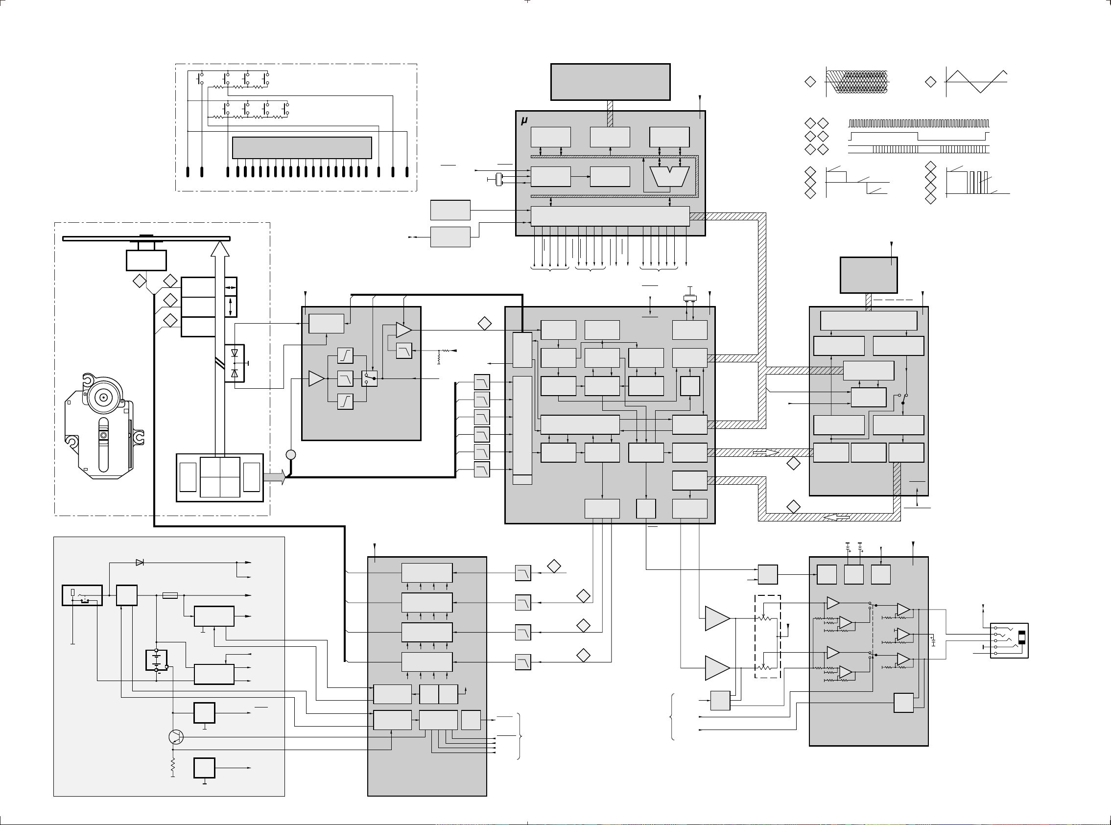
BLOCK DIAGRAM
DISC
a
t
b
n
r
u
t
DA23-L(N)PH
CD-DRIVE
SUPPLY/CHARGE CIRCUIT
DC-in socket
+
PCS 107 233
l
e
TURNTABLE
+A STAB.
MOTOR
ACCU or
BATTERY
T630mA
+
CHARGE
SWITCH
GND2
1
1012
TRACK
SERVO
9
FOCUS
SERVO
11
SLIDE
SERVO
PHOTO DIODE
ARRAY
charge
PLAY
PREVSTOP
R11 R12 R13
R1 R2 R3 R4
PLAY
KEY2
CD
BA
DC/DC
CONVERTER
RECH. BATT.
MEASURING
PART
ACCU
DETECT.
TEMP.
DETECT.
3-3 3-3
DBB
NEXT
MEMBRANE-KEYBOARD & LCD
PROG
ESP
MODE
LCD
(connected via zebra-strip)
+2.6V
VCC2, VCCL
LASER
LD
SUPPLY &
PROTECT.
Laser
diode
Monitor
diode
MON
DIN
TZA1024
HF-PREAMPLIFIER
SUM (A + B + C + D)
+
EF
FLEX
+DC
DC_IN
(TO m P)
+A
+2.6V
DM_PWM
(FROM m P)
BATT_LEVEL
(TO m P)
CHG_DET
(TO m P)
ACCU
(TO m P)
TEMP
(TO m P)
1x
4x
2x
GND1
KEY1
VDD
24
RC (FROM/TO
RC-SOCKET)
EQSEL
PWRON
CDRW
+DC
DCIN
DM±
SL±
Focus±
Track±
VC
VOUT
VIN
RF2
CHGSW
RS
DC/DC
CONVERTER
CONST.VOLT.
CURRENT &
CHARGE
MOTOR DRIVER 2
MOTOR DRIVER 4
MOTOR DRIVER 1
MOTOR DRIVER 3
SC111259FTA
SERVO DRIVER &
POWER MGT. IC
RESET (FROM
SERVO DRIVER)
MEMBRANE
KEYBOARD
RC-CIRCUIT
RFEQO
CMFB
RFFB
H-BRIDGE
H-BRIDGE
H-BRIDGE
H-BRIDGE
SAW
SAW
GEN.2
GEN.1
CONTROL RESET
+2.6V
SAWVG VLG VR
SAWVG VLG VR
SAWVG VLG VR
SAWVG VLG VR
1)
(TO NPC)
E
F
B
A
C
D
SAW
YFLAG
1
DM_IN
SLIDE_IN
FOCUS_IN
TRACK_IN
RESET
4MHz
HFIN
R1
R2
D1
D2
D3
D4
RESET
S_MUTE
CHGON
SLEEP
WAKE
P TMP86C829
CLOCK GEN.
& TIMING
RC
ACCU
CHG_DET
BAT_LEVEL
FROM/TO SUPPLY/
CHARGE CIRCUIT
FRONT END TIMING
DIGITAL PLL
VERSATILE
INTERFACE
EFM
DEMOD.
A/D-CONVERTER
PRE-PROC.
Vref
SAA7324H
CD10
FROM/TO m P
16
(PWM signal)
SL
(PWM signal)
FO
RA (PWM signal)
L.P.F.
L.P.F.
L.P.F.
L.P.F.
TEMP
DC_IN
S_MUTE
CHG_ON
TO SERVO &
POWER MGT.
INTERFACE
CORRECT.
CONTROL PART
FUNCTION
CONTROL
DM_PWM
(FROM m P)
15
13
14
LCD
F
LCD DRIVER
16bit TIMER
COUNTER
I/O PORTS
WAKE
SLEEP
EBU
ERROR
SRAM
OUTPUT
STAGES
SL FO RA KILL
PORES
(TO NPC)
(TO CD10)
NPC_RESET
CONTROL
ADDRESS.
PROCESS.
BEEP
TO HEADPHONE AMP.
PORES
(FROM m P)
RESET
MOTOR
RAM
AUDIO
KILL
DBB_ON
DBB_STEP
ROMRAM
ALU
MUTE
LF_POW
SUBCODE
PROCESS.
INTERFACE
INTERFACE
LOOPBACK
BITSTREAM
DBB_STEP
FROM m P
DM_PWM
(TO SERVO)
8.4MHz
PEAK
DET.
m P
SERIAL
SERIAL
DAC
DBB_ON
BEEP
> 800 mVpp
eye-pattern signal
1
+2.6V
AVDD
YMLD
YMCLK
YMDATA
SILD
RAB
SCL
SDA
SFSY
SCLK
2
5
WCLK
3
6
DAT A
4
7
3V
10
0
11
-3V
12
TB=0.5m s
TRANSFER OF AUDIO SAMPLES VIA SERIAL INTERFACE CD10 ´ NPC
left channel
MSB
servo in or
disc motor cw
not moving
servo out or
disc motor ccw
+2.6V
DRAM
+2.6V
VDD VDD
A0...A10, D0...D3
CAS, RAS, WE, OE
DRAM INTERFACE
SBSY
SFSY
SILD
RAB
SCL
SDA
YMLD
YMCLK
YMDATA
ZSENSE
SBSY
YFLAG
(FROM
CD10)
CONTROLLER
INTERFACE
SHOCK
CONTROL
DECODERENCODER
ATTENUATORINPUT BUFFER
SCLK
WCLK
DATA
SCLI
WCLI
SDI
YSCK
YLRCK
YSRDATA
2-4
INPUT
INTERFACE
EXTENSION
SM5903BF
I/O
NPC
ZSCK
ZLRCK
ZSRDATA
LF_POW
(FROM m P)
POW.
SW.
E_KILL
MUTE
(FROM m P)
MUTE
CONT.
5-7
Switch
MUTE
RIPPLE
FILTER
VOLUME
IN A
Vref
IN B
Low-pass
boost
DBB
DBB
CONT.
Switch
Beep in
BA3574BFS
HEADPHONE AMP.
VCC
OUTPUT
INTERFACE
RESET
NPC_RESET
(FROM m P)
+A
BEEP
LSB
+2.6V
VCC
during focus search
2,5V
0
9
-2,5V
right channel
MSB
13
3V
14
15
0
16
LEFT
Vref
RIGHT
1)
TB=0.1s
LSB
servo out or disc motor cw
not moving
servo in or
disc motor ccw
RC
(FROM/TO
RC-CIRCUIT)
HEADPHONE&
RC-SOCKET
not on all versions
Page 15
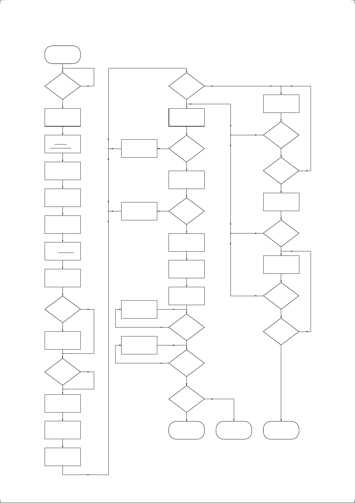
START-UP PROCEDURE
3-4
POWER OFF
(stand-by)
PLAY
pressed ?
Y
DC/DC converter
is switched on
(via WAKE)
m P resets
CD10 and NPC
PORES=L
NPC_RESET=L
m P initializes
CD10 and NPC
with default
parameter/settings
m P switches
headphone amplifier
on (via LF_POW)
m P outputs servo
signal for disc motor
(DM_PWM 50% duty)
m P switches
servo driver on
(via S_MUTE)
m P sends
command to CD10:
“move slide inside”
Start-up procedure for ext.DC supply,
no accu inserted, hold-switch in off pos.,
ESP on, resume-mode off, CD-door closed.
N
re-initialize CD10
and restart focus
search procedure
re-initialize CD10
and restart focus
search procedure
focus found
during ramping
m P calculates
ramping offset and
sends play-params
to CD10
N
stability test
m P accelerates
disc to nom. speed
(~330ms)
disc at nom.
N
speed within
m P initializes
radial servo loop
cycle ?
m P releases
(via MUTE)
cycle ?
Y
focus
ok ?
~10s ?
muting
N
m P sends new focus
parameters to CD10
(switch to higher
focus sensitivity)
focus found
Y
during ramping
cycle ?
N
Y
Y
already
looped through
all (4) focus
sensitivities
?
switch back to
normal focus
sensitivity
focus found
Y
during ramping
N
m P sends new focus
parameters to CD10
(switch to higher
focus sensitivity)
N
Y
inner switch
closed within
~6s ?
Y
m P sends
command to CD10:
“move slide outside”
inner switch
open within
~0.25s ?
Y
m P sends
commands to CD10:
“slide servo off”
m P accelerates
disc motor for
~200ms
m P sends
commands to CD10:
“laser on”
“focus servo on”
m P sends command
to CD10: “jump
10 tracks inside”
N
N
radial
error handler
subcode
error handler
N
N
jump
ok ?
Y
subcode
ok ?
Y
TOC
found within
~30s ?
Y
PLAY-MODE
N
display shows
“nF d1SC”
start-up stopped
Y
during ramping
looped through
display shows
start-up stopped
focus found
cycle ?
N
already
all (4) focus
sensitivities
?
Y
“no d1SC”
N
PCS 107 234
Page 16

3-5
PIN DESCRIPTION OF INTEGRATED CIRCUITS
TZA1024 – HF-PREAMPLIFIER AND LASER SUPPLY CIRCUIT
Pin Name Direction Description
–––––––––––––––––––––––––––––––––––––––––––––––––––––––––––––––––––––––––––––––––––––––––––––––––––––––––––
1 LD HF-preamp Æ CD-drive current output to laser diode
2 VCCL +2.6V laser supply voltage
3 CFIL Æ HF-preamp external filter capacitor
4 MON CD-drive Æ HF-preamp laser monitor diode input
5 DIN CD-drive Æ HF-preamp central diode input
6 GND
7 PWRON CD10 Æ HF-preamp power-on select input
8 CMFB +2.6V / 2 common mode feedback voltage input
9 RFFB Æ HF-preamp external RF feedback resistor
10 RFEQO HF-preamp Æ RF amplifier output
11 CDRW CD10 Æ HF-preamp gain select input for CDDA/CDRW
12 EQSEL CD10 Æ HF-preamp equalizer/speed select input
13 VCC2 +2.6V supply voltage
14 RGADJ GND external laser supply gain adjust resistor
SC111259FTA – SERVO DRIVER & POWER MANAGEMENT IC
Pin Name Direction Description
–––––––––––––––––––––––––––––––––––––––––––––––––––––––––––––––––––––––––––––––––––––––––––––––––––––––––––
1 SLEEP µP Æ servo driver sleep input
2 WAKW µP Æ servo driver wake input
3 VR +VR reference voltage input (motor driver)
4 ERR4 CD10 Æ servo driver control signal input (slide error signal)
5 CF4 Æ servo driver phase correction capacitor connect (CH4)
6 CF3 Æ servo driver phase correction capacitor connect (CH3)
7 ERR3 CD10 Æ servo driver control signal input (radial error signal)
8 ERR2 CD10/µP Æ servo driver control signal input (disc speed error signal)
9 CF2 Æ servo driver phase correction capacitor connect (CH2)
10 CF1 Æ servo driver phase correction capacitor connect (CH1)
11 ERR1 CD10 Æ servo driver control signal input (focus error signal)
12 OUT1A servo driver Æ CD-drive positive drive output (CH1)
13 PGND1 GND H-bridge driver ground
14 OUT1B servo driver Æ CD-drive negative drive output (CH1)
15 VIN12 +A CH1 and CH2 H-bridge driver supply voltage
16 OUT2B servo driver Æ CD-drive negative drive output (CH2)
17 PGND2 GND H-bridge driver ground
18 OUT2A servo driver Æ CD-drive positive drive output (CH2)
19 OUT3A servo driver Æ CD-drive positive drive output (CH3)
20 PGND2 GND H-bridge driver ground
21 OUT3B servo driver Æ CD-drive negative drive output (CH3)
22 VIN34 +A CH3 and CH4 H-bridge driver supply voltage
23 OUT4B servo driver Æ CD-drive negative drive output (CH4)
24 PGND4 GND H-bridge driver ground
25 OUT4A servo driver Æ CD-drive positive drive output (CH4)
26 VG +VG charge pump output
27 C2H Æ servo driver charge pump capacitor connect
28 C1H Æ servo driver charge pump capacitor connect
29 C1L Æ servo driver charge pump capacitor connect
30 C2L Æ servo driver charge pump capacitor connect
31 VIN battery Æ servo driver battery supply voltage
32 RSTB servo driver Æ µP reset block output
33 CHGSW servo driver Æ charge circuit transistor drive output for battery charger
34 RS charge circuit Æ servo driver OpAmp non-inverting input for battery charger
35 INM2 +A stabilizer Æ servo driver error amplifier inverting input
36 RF2 +A stabilizer Æ servo driver error amplifier output
37 DCIN +DC DC power supply from AC/DC adaptor
38 VDET servo driver Æ DCIN over voltage and VIN low voltage detect output
39 VREF servo driver Æ Voltage reference circuit output
40 DTC Æ servo driver max. duty control voltage input for power management
41 VOUT servo driver Æ DC/DC converter PWM output for power management
42 VC Æ servo driver power management power supply
43 CGND GND internal ground
44 RF1
45 INM1 Æ servo driver OpAmp inverting input for power management
46 CLK Æ servo driver clock input
47 OE µP Æ servo driver output enable for motor drivers
48 CHGON µP Æ servo driver charge enable for battery charger
GND ground
servo driver
Æ OpAmp output for power management
PCS 107 235
Page 17

3-6
SAA7324 – DECODER, DIGITAL SERVO IC AND D/A-CONVERTER CD10 (low voltage version)
Pin Name Direction Description
–––––––––––––––––––––––––––––––––––––––––––––––––––––––––––––––––––––––––––––––––––––––––––––––––––––––––––
1 HFREF Æ CD10 comparator common mode input
2 HFIN Æ CD10 comparator signal input
3 ISLICE CD10 Æ current feedback from data slicer
4 VSSA1 GND analog ground 1
5 VDDA1 +2.6V analog supply voltage 1
6 IREF CD10 Æ reference current output pin
7 VRIN CD10 Æ reference voltage for servo ADC’s
8 D1 CD-drive Æ CD10 unipolar current input (central diode signal input)
9 D2 CD-drive Æ CD10 unipolar current input (central diode signal input)
10 D3 CD-drive Æ CD10 unipolar current input (central diode signal input)
11 D4 CD-drive Æ CD10 unipolar current input (central diode signal input)
12 R1 CD-drive Æ CD10 unipolar current input (satellite diode signal input)
13 R2 CD-drive Æ CD10 unipolar current input (satellite diode signal input)
14 VSSA2 GND analog ground 2
15 CROUT CD10 Æ X-TAL crystal/resonator output
16 CRIN X-TAL Æ CD10 crystal/resonator input
17 VDDA2 +2.6V analog supply voltage 2
18
LN CD10
19 LP CD10 Æ DAC left channel differential output - positive
20 VNEG GND DAC negative reference input
21 VPOS +2.6V DAC positive reference input
22 RN CD10 Æ DAC right channel differential output - negative
23 RP CD10 Æ DAC right channel differential output - positive
24 SELPLL CD10 Æ selects whether internal clock multiplier PLL is used
25 TEST1 GND test control input 1; this pin should be tied low
26 CL16 CD10 Æ NPC 16.9344 MHz system clock output
27 DATA CD10 Æ NPC serial data output (3-state)
28 WCLK CD10 Æ NPC word clock output (3-state)
29 SCLK CD10 Æ NPC serial bit clock output (3-state)
30 EF CD10 Æ NPC C2 error flag output (3-state)
31 TEST2 GND test control input 2; this pin should be tied low
32 KILL CD10 Æ Mute control kill output (programmable; open-drain)
33 VSSD1 GND digital ground 2
34 V2/V3 CD10 Æ NPC versatile I/O: input versatile pin 2 or output versatile pin 3 (open-drain)
35 WCLI NPC Æ CD10 word clock input (for data loopback to DAC)
36 SDI NPC Æ CD10 serial data input (for data loopback to DAC)
37 SCLI NPC Æ CD10 serial bit clock input (for data loopback to DAC)
38 RESETn µP Æ CD10 power-on reset input (active low)
39 SDA µP ´ CD10 microcontroller interface data I/O line (open-drain output)
40 SCL µP Æ CD10 microcontroller interface clock line input
41 RAB µP Æ CD10 microcontroller interface R/W and load control line input (4-wire bus mode)
42 SILD µP Æ CD10 microcontroller interface R/W and load control line input (4-wire bus mode)
43 STATUS CD10 Æ servo interrupt request line/decoder status register output (open-drain)
44 TEST3 GND test control input 3; this pin should be tied low
45 RCK Æ CD10 subcode clock input
46 SUB CD10 Æ P-to-W subcode bits output (3-state)
47 SFSY CD10 Æ µP subcode frame sync output (3-state)
48 SBSY CD10 Æ NPC subcode block sync output (3-state)
49 CL11/4 CD10 Æ 11.2896 MHz or 4.2336 MHz (for microcontroller) clock output
50 VSSD2 GND digital ground 3
51 DOBM CD10 Æ bi-phase mark output (externally buffered; 3-state)
52 VDDD1P +2.6V digital supply voltage 2 for periphery
53 CFLG CD10 Æ correction flag output (open-drain)
54 RA CD10 Æ servo driver radial actuator output
55 FO CD10 Æ servo driver focus actuator output
56 SL CD10 Æ servo driver slide control output
57 VDDD2C +2.6V digital supply voltage 3 for core
58 VSSD3 GND digital ground 4
59 MOTO1
60 MOTO2
61 V4 CD10 Æ HF-preamp versatile output pin 4
62 V5 CD10 Æ HF-preamp versatile output pin 5
63 V1 innerswitch Æ CD10 versatile input pin 1
64 LDON CD10 Æ HF-preamp laser drive on output (open-drain)
Æ DAC left channel differential output - negative
CD10
Æ servo driver motor output 1; versatile (3-state)
Æ motor output 2; versatile (3-state)
CD10
PCS 107 236
Page 18

3-7
SM5903BF – COMPRESSION-TYPE ANTI-SHOCK MEMORY CONTROLLER NPC
Pin Name Direction Description
–––––––––––––––––––––––––––––––––––––––––––––––––––––––––––––––––––––––––––––––––––––––––––––––––––––––––––
1 VDD +2.6V supply voltage
2 UC1 NPC ´ µP interface extension I/O line 1
3 UC2 NPC ´ µP interface extension I/O line 2
4 UC3 NPC ´ µP interface extension I/O line 3
5 UC4 NPC ´ µP interface extension I/O line 4
6 UC5 NPC ´ µP interface extension I/O line 5
7 TEST1/DIT NPC Æ digital audio interface output
8 TEST2 +2.6V test pin
9 CLK CD10 Æ NPC 16.9344MHz clock input
10 VSS GND ground
11 YSRDATA CD10 Æ NPC audio serial data input
12 YLRCK CD10 Æ NPC audio serial L/R clock input
13 YSCK CD10 Æ NPC audio serial bit clock input
14 ZSCK NPC Æ CD10 audio serial bit clock output
15 ZLRCK NPC Æ CD10 audio serial L/R clock output
16 ZSRDATA NPC Æ CD10 audio serial data output
17 YFLAG CD10 Æ NPC signal processor IC RAM overflow flag
18
YFCLK GND crystal-controlled frame clock input
19 YBLKCK CD10 Æ NPC subcode block clock signal output
20 RESET µP Æ NPC system reset input (active low)
21 ZSENSE NPC Æ µP interface status output
22 VDD2 +2.6V supply voltage
23
24 YMLD µP Æ NPC µP interface latch clock input
25 YMDATA µP Æ NPC µP interface serial data input
26 YMCLK µP Æ NPC µP interface shift clock input
27 OE NPC Æ DRAM DRAM OE control output (active low)
28 CAS NPC Æ DRAM DRAM CAS control output (active low)
29 D2 NPC ´ DRAM DRAM data input/output 2
30 D3 NPC ´ DRAM DRAM data input/output 3
31 D0 NPC ´ DRAM DRAM data input/output 0
32 D1 NPC ´ DRAM DRAM data input/output 1
33 WE NPC Æ DRAM DRAM WE control output (active low)
34 RAS NPC Æ DRAM DRAM RAS control output (active low)
35 A9 NPC Æ DRAM DRAM address output 9
36 A8 NPC Æ DRAM DRAM address output 8
37 A7 NPC Æ DRAM DRAM address output 7
38 A6 NPC Æ DRAM DRAM address output 6
39 A5 NPC Æ DRAM DRAM address output 5
40 A4 NPC Æ DRAM DRAM address output 4
41 A0 NPC Æ DRAM DRAM address output 0
42 A1 NPC Æ DRAM DRAM address output 1
43 A2 NPC Æ DRAM DRAM address output 2
44 A3 NPC Æ DRAM DRAM address output 3
Æ NPC forced mute input
YDMUTE
PCS 107 237
Page 19
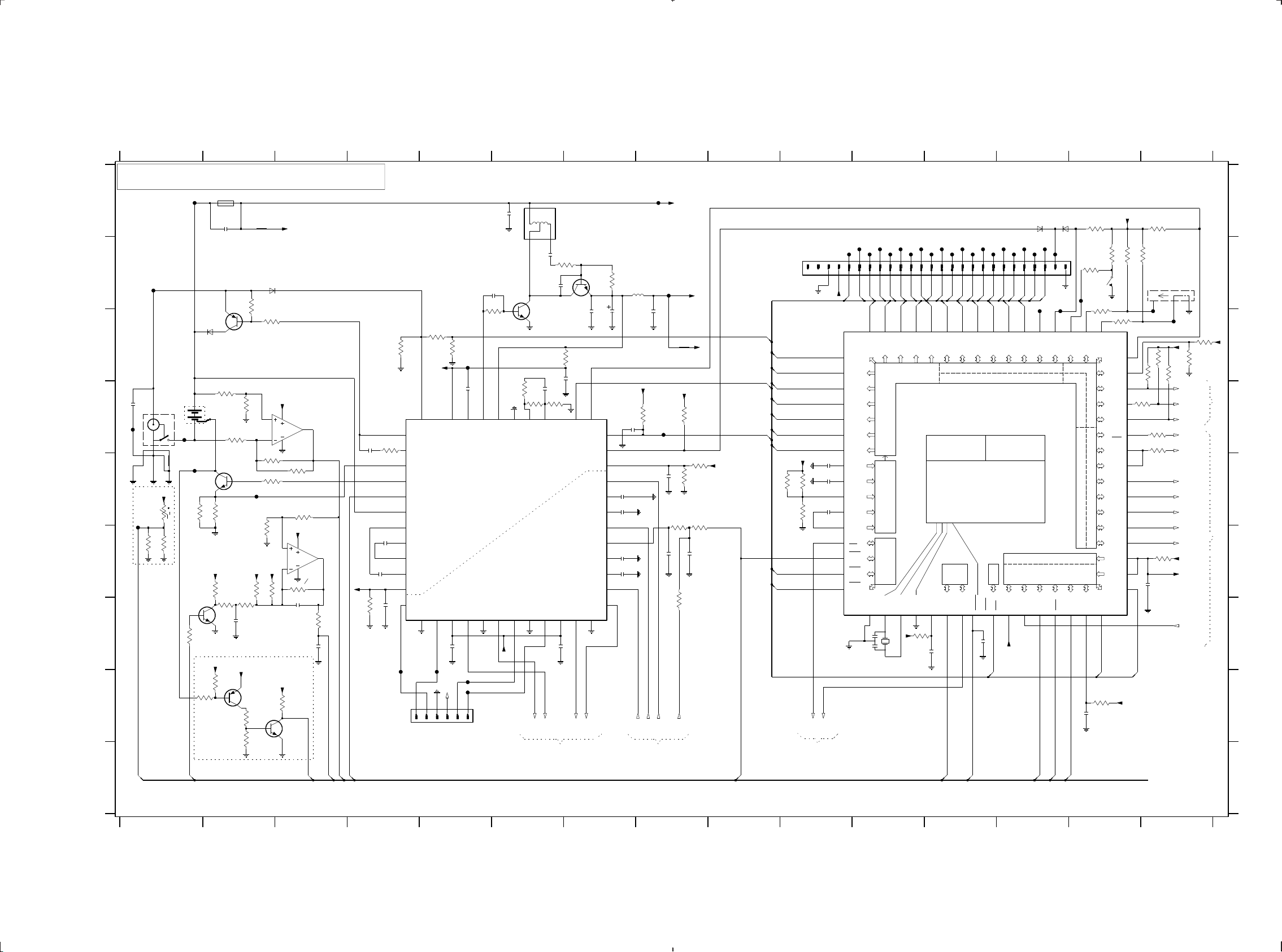
4-1 4-1
CONTROL / SUPPLY PART - CIRCUIT DIAGRAM
1250 H4
1251 A2
1252 D1
1400 B10
1401 B14
1402 B15
1403 G11
2250 A6
2251 A2
2252 B6
2253 B6
2255 C7
2256 C7
2257 C8
2258 D5
2259 C6
2260 D6
1 2
2261 D1
2262 D4
2263 E7
2264 E7
2265 F4
2266 F7
2267 F4
2268 F7
2269 G4
2270 G3
2271 G2
2272 G5
2273 G6
2274 G3
2275 F8
2276 F8
2277 E8
2278 D7
3 4
CONTROL / SUPPLY-PART
1251
+2.6V
150K
F252
T630mA
SP391
2251
1u
6252
SB140
3258
100K
F261
F253
M
7255
C
C
C
3271
3284
C
3286
t
10K
2R7
7258
C
BC847BW
C
3287
10K
+2.6V
3270
2R7
3272
4K7
3276
18K
ACCU_IN DETECTION - SE40
+A
3279
2M2
3280
C
470K
BC869
3264
100K
C
C
C
C
7252
BC868
3273
100K
3277
18K
2271
1u
+A
3251
270R
3259
68K
F254
3265
330K
+1.25V
3274
C
100K
C
C
7259
C
BC857BW
3282
470K
3283
470K
6251
BAT254
C
+2.6V
C
C
C
3253
270R
3
2
3267
68K
3293
330R
VCC-M
+2.6V
C
+2.6V
7254-A
8
TC75W51FU
4
3296
1M
3263
22K
+2.6V
5
6
4
3275
330K
2270
470p
3281
C
47K
7260
C
BC847BW
1
X
C
7254-B
8
TC75W51FU
0R for
non charging
C
C
2274
1n
7
3278
10K
A
B
F251
C
2261
1252
100n
D
F250
E
DC JACK
ESD
TEMP.
F426
X
3285
F
G
H
2262
3n3
2267
100n
3294
470K
2265
100n
2701 H14
3250 B7
3251 B2
3252 B6
3253 C2
3254 C5
3,4V
3266
10K
0V
0V
2,6V
4,4V
1,2V
5,5V
7,4V
8,4V
2269
100n
2400 F15
2401 G12
2402 E10
2403 E10
2404 E10
2405 G12
+VG
C
0,4V
1,4V
2,2V
B-ZR
1250
3261
F257
10K
3255 C5
3256 C6
3257 D6
3258 D2
3259 D2
3260 D6
3261 C4
3263 E3
3264 D2
3265 F2
3266 D4 3417 C15
3267 E2
5 6
3254
10K
3255
47K
+1.25V
2,6V
4,8V
37
RF236
DCIN
INM235
RS34
CHGSW33
RSTB32
VIN31
C2L30
C1L29
C1H28
C2H27
VG26
OUT4A25
24
2,2V
0V
M
F258
2
1
SL+
SL-
F262
1,2V 0,2V 0,3V
39
38
40
VREF
VDET
SUPPLY MANAGER
VIN34
OUT4B
PGND4
22
21
23
4,4V
2,3V
2272
1u
M
F259
F260
INNERSWITCH
M
6
3 4 5
DM+
DM-
3268 E8 3419 C15
3269 E8
3270 E2
3271 E1
3272 F2
3273 F2
3274 F2
3275 F3
3276 G2
3277 G2
3278 G3
3279 H2
3280 H2
3281 H3
3282 H2
3283 H2
3284 E1
3286 F1
3288 B7
3289 E8
3290 G8
3291 D8
3292 D8 F401 B13
3293 E2
3294 G4
3295 D6
3296 E3
7 12 13 14
5251
10u
2.6V-D
3292
10K
2278
1u
Focus
Radial
to CD-PART
F255
2257
4u7
F263
Sledge
F256
2275
2250
4u7
2254
4n7
3252
0V
330R
2258
1u
DTC
3257
220K
2,6V
41
42
43
VC
VOUT
SERVODRIVER
PGND3
OUT3A
OUT3B
20
19
2,2V
1,2V
M M
VCC-M
4 6
5250
6RG
40uH
3
12
2253
22n
2252
330p
4,4V
BC337-40
7251
BC368
2260
100p
3260
1M
3295
270K
0,6V
1,6V
44
45
46
RF1
INM1
CGND
PGND2
OUT2A18OUT2B
17
15
16
1,8V0V0V
4,4V
Track-
Track+
to 1830 CD-PART
3288
10R
X
0V
2273
1u
M
7250
3256
4K7
2259
10n
47
CLK
VIN12
14
2,3V
2255
1u
2,6V
OE
OUT1B
Focus-
0V
48
CHGON
SLEEP 1
WAKE 2
ERR4 4
ERR3 7
ERR2 8
ERR1
OUT1A 12
PGND1
M
13
0V
Focus+
3250
680R
2256
100u
7256
MPC17A253
0V
4,4V
1,3V
VR 3
1,3V
CF4 5
1,3V
CF3 6
1,3V
1,3V
1,5V
CF2 9
1,3V
CF1 10
1,3V
11
0V
2,2V
2263
220p
2264
220p
2266
220p
2268
220p
3401 B14
3403 B14
3404 B14
3405 B14
3406 C14
3407 E10
3408 E10
3409 E10
3410 G11
3411 F15
3412 D15
8 9 10 11
+A
+2.6V
DC_IN
S_MUTE
SLEEP
2277
1u
3901
10K
2.6V-D
+A
3291
100K
3268
+VR
%
10K
3269
%
10K
3289
5K6
2276
10n
100n
3290
X
5K6
DM
3413 D15
3414 A15
3415 C15
3416 C15
3418 C15
S2
S1
S0
C3
C2
C1
C0
2.6V-D
3407
3408
150K
12K
3409
5K6
S_MUTE
SLEEP
to AUDIO-PART
6251 B2
6252 C2
6400 A13
6401 A13
7250 B7
7251 C6
F407
F400
24
2526 3
Key1
C3
+AVDD
7400
TMP86C829F
1,3V
49
SEG2
1,3V
50
SEG1
1,3V
51
SEG0
1,3V
52
COM3
1,3V
53
COM2
1,3V
54
COM1
1,3V
55
COM0
56
2402
V3
2,6V
100n
57
2403
V2
1,7V
100n
58
0,9V
V1
2404
59
C1
0,7V
100n
60
1,5V
C0
1,3V
61
P30
DV0
1,5V
PD03
62
P31
TC3
2,6V
PD04
63
P32
TC4
0V
PD06
64
P33
TC6
D
4.233MHZ
MUTE
D
3420 D15
3701 H14
3901 E8
5250 B6
5251 B7
1400
ESD
D
D
BEEP
7252 C2
7254-A D3
7254-B F3
7255 E2
7256 D7
7258 G13285 F1
F411
F409
F408
F410
F412
C2
C1
C0S9S2
S6
S5
S4
S3
1,3V
48 47 46 45 44
1 2 3
0V
CST
{C0,C1,C2,C3,S0,S1,S2,S3,S4,S5,S6,S7,S8,S9,S10,S11,S12,S13,Key1,Key2,S_MUTE,SLEEP,DC_IN}
SEG3
SEG4
LCD - DRIVER
LCD VOLTAGE
BOOSTER CIRCUIT
P3
XIN
VSS
1,0V 1,1V0V2,6V
1403
1,3V1,3V1,3V
SEG5
XOUT
4
2.6V-D
F413
SEG6
S13
7259 H2
7260 H33287 G1
7400 C10
F250 D1
F251 B1
F252 A13400 A14
F414
S10
S7
SEG7
F253 E1
F254 E23402 B14
F255 A8
F256 B8
F257 H4
F258 H5
F417F415
F416
F418
10111213141516171819220212223
S0
S1
S11
S12
S9
S8
1,3V1,3V
S10
1,3V1,3V
P77
P76
SEG8
SEG9
F259 H5
F260 H5
F261 D1
F262 C5
F263 D8
F400 B102254 B6
F421
F419
F422
F420
S3S4S5S6S8
S12
S11
P75
P74
P73
SEG10
SEG11
LCD - DRIVER
I/O PORT P7
TMP86C829
ROM RAM
8-BIT-CPU
VDD
XTOUT
XTIN
P21
TEST
5 11 12 13 14 15 16
6 7
2,6V
3410
10R
D
2401
4u7
D
0V 2,6V
P20
STOP
INT5
RESET
P22
8
D
2405
3,2V
9
100n
DC_IN
P60
10
1,3V 1,5V
+RCREF
4,4V
BAS216
F423
F424
S7
S13
P72
SEG12
SEG13
8 BIT A/D Converter
ADC INPUT I/O PORT P6P2P2
ECIN
P61
2,6V
6400
456789
F401
F402
P71
P62
Key2
3637383940414243
SEG14
ECNT
1,8V
F402 B13
F403 B13
F404 B14
F405 C15
F406 C15
6401
BAT254
F427
F403
P70
SEG15
INT0
P63
1,4V
1
D
P57
P64
2701
F407 B11
F408 B11
F409 B11
F410 B11
F411 B11
F412 B11
3400
2,7V4,3V
100K
3404
1K
SPPB51
F404
2,6V0V2,7V0V1,3V1,3V1,3V
P56
SEG16
SEG17
I/O PORT P5
I/O PORT P1
STOP2
P65
STOP3
1,4V 2,6V
1n
D
3401
220K
1
1401
2
D
3405
3406
1K
2,6V
333435
P55
SEG18
P54
SEG19
P53
SEG20
P52
SEG21
P51
SEG22
LCD - DRIVERLCD - DRIVER
P50
SEG23
P17
SEG24
SCK
P16
SEG25
TXD/SO
SEG26
P15
RXD/SI
SEG27
P14
INT3
SEG28
P13
INT2
SEG29
P12
INT1
SEG30
P11
SEG31
P10
AVDD
VAREF
STOP5
P67
P66
STOP4
Key2
3701
100K
2.6V-D
1K
F413 B11
F414 B12
F415 B12
F416 B12
F417 B12
F418 B12
3402
220K
chg_on
32
0V
31
2,6V
30
2,0V
3420
29
2,4V
2K7
28
1,6V
27
1,9V
26
1,8V
25
1,8V
2,6V
24
2,6V
23
2,6V
22
21
0,3V
2,6V
20
19
2,6V
18
2,6V
17
2,6V
Key1
2.6V-D
3414
47K
3403
220K
1402
1 2 3 4
F405
3416
10K
3415
3412
100R
3413
100R
3411
10R
2400
1u
D
F419 B12
F420 B12
F421 B13
F422 B13
F423 B13
F424 B13
15
ESD-11H130
F406
2.6V-D
4K7
3417
10K
LF_POW
DBB_STEP
DBB_ON
SCL
SDA
PORES
NPC_RESET
YMLD
RAB
SILD
2.6V-D
+AVDD
SFSY
D
3419
0R
D
F426 E1
F427 B13
3418
0R
L
LN
2.6V-D
A
B
C
D
to AUDIO-PART
E
to CD-PART
F
G
H
TEMP
I
C....only for charging version
E....only for DORIS2 (ESP)
X....component only foreseen (not in use)
%....tolerance 1%
1
DM_PWM
2 3
ACCU
CHG_DET
BATT_LEVEL
RESET
4 5
6 7 8 9
DM_PWM
RESET
ACCU
10 11 12 13
BATT_LEVEL
CHG_DET
TEMP
{TEMP,ACCU,BATT_LEVEL,CHG_DET,RESET,WAKE,DM_PWM}
14 15
I
PCS 107 238
Page 20
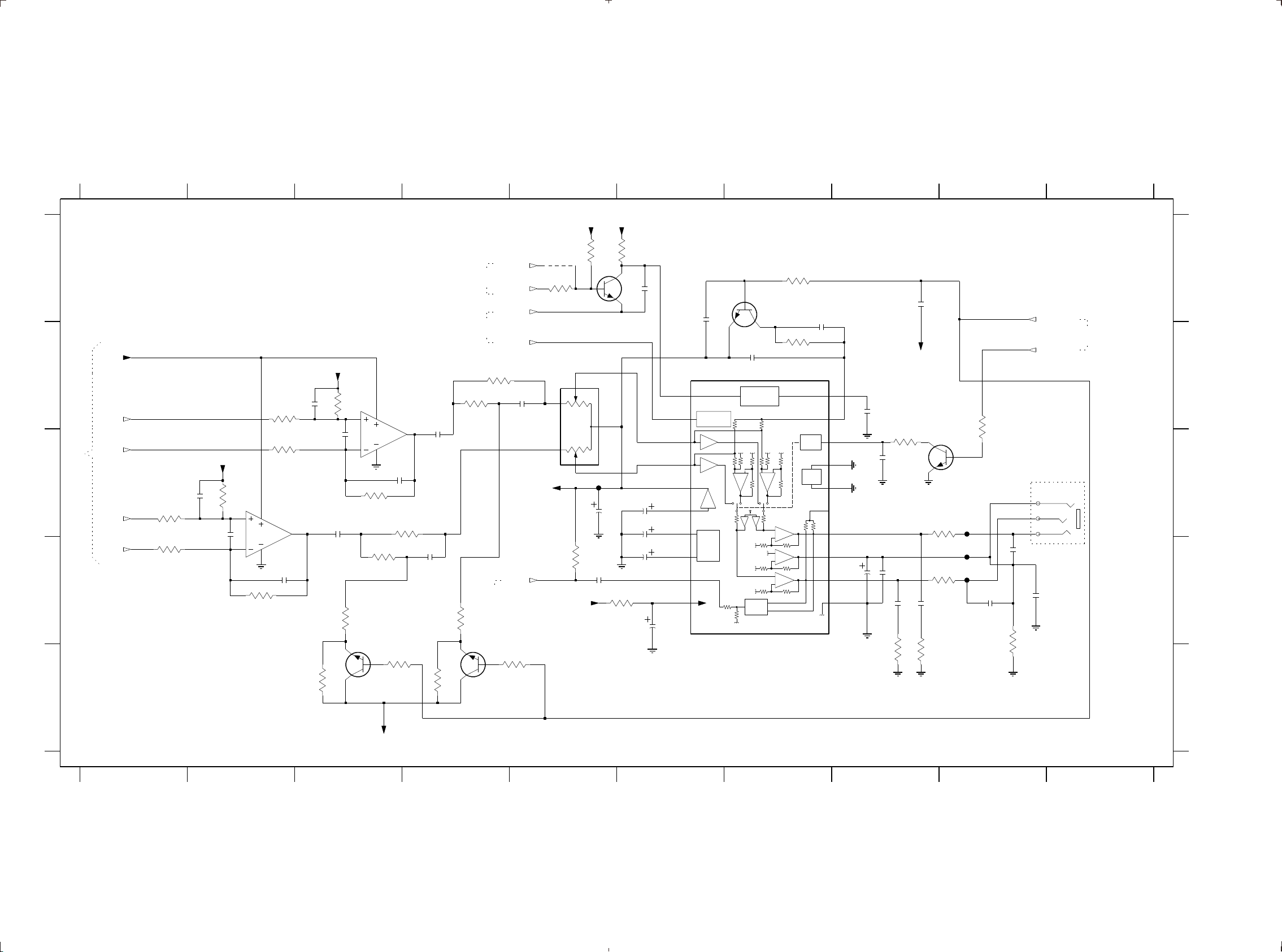
AUDIO PART - CIRCUIT DIAGRAM
4-2 4-2
A
B
C
D
E
1300 C10
2300 B3
2301 C2
2302 C3
2303 D2
2304 C3
2307 D4
2308 B4
2309 C3
2310 A6
2311 C5
2312 C6
2313 C6
1 2 3
AUDIO-PART
+Audio
RP
RIGHT Channel
RN
from CD-PART
LP
LEFT Channel
LN
3301
33K
3303
33K
2301
220p
2303
100p
VREF
1,3V
1,3V
2314 D6
2315 D5
2316 D6
2317 B7
2318 B8
3305
15K
5
6
A
3309
15K
3300
33K
3302
33K
2,5V
7300-B
8
TC75W51FU
4
2305
220p
2319 C8
2320 D82305 D2
2321 D8
2322 D8
2323 D8
2300
7
1,3V
220p
2325 D9 3325 E8
2326 D9
2327 A7
2328 A6
2892 A8
3300 B2
3301 C12306 B5
3302 C2
3303 D1
3304 B3
3305 C2
3306 D4
3307 D3
3308 C3
3309 D2
3310 B4
3311 D3
3312 E4
3313 E3
3314 E5
3315 E3
3316 A5
3317 A5
3318 C8
4 5
+2.6V
+2.6V
X
3331
10K
X
PART
3320
RK10J
VREF
PART
3332
3317
4K7
4
5
3
2x10K
2
0,8V
7303
BC847BW
7
1
6
F304
2311
22u
A
3335
4K7
2315
100n
+A
2310
A
3319
2R2
VREF
1,3V
1,3V
2309
4u7
3313
1M
3304
15K
2302
3
100p
2
A
3307
2K2
1,9V
BC847BW
1,9V
3308
15K
3311
1,3V
7301
7300-A
2,7V
TC75W51FU
8
4
2304
220p
5K6
3315
3K3
1,3V
3333
18K
E_KILL
from CD-PART
from CONTROL
3310
5K6
2308
1
4u7
2307
3n3
3306
2K2
1,9V
3312
1M
1,9V
KILL
MUTE
LF_POW
3334
18K
2306
3n3
BEEP
from CONTROL
3314
1,3V
3K3
BC847BW
7302
3316
10K
0V
1u
2313
1u
3319 D6
3320 B5
3321 B9
3322 C9
3323 D9
6 7
2312
2u2
2314
22u
2316
220u
3324 E8
3327 B7
3328 A7
3330 D9
2328
100n
2317
7305
BA3574BFS
Switch
11
0V
12
Power on
Switch
2,0V
13
+
1,3V
in
14
+
1,3V
in
out
15
1,3V
BIAS
16
in
1,3V
RF out
17
4,2V
Ripple
Filter
18
1,2V
RF in
19 2
Beep in
1,3V
Vcc
20
4,4V
1,7-3,6V
100n
+ - + -
+ +
27k
2k
BC847BW
MUTE
Beep
43k43k
3331 A52324 D9
3332 A5
3333 C4
3334 B4
3335 D5
3328
47K
7307
3327
+
+
-
+
-
2327
100n
1M
time
Low-pass
boost
DBB
Switch
time
AVC
Mix out
in
out
Vref
out
7300-A B3
7300-B C2
7301 E3
7302 E4
7303 A5
10
9
1,3V
8
0,7V
7
0V
6
0V
5
1,3V
4
1,3V
3
1,3V
1,3V
1
0V
0,7V
A
A
A
2320
2318
1u
A
2u2
8
A
2319
1u
2321
1u
A
7305 B6
7306 C9
7307 A7
F300 C9
F301 D9
3318
100K
2323
100n
3325
2R2
2892
4u7
VREF
7306
BC847BW
A
3322
1R
3323
1R
2322
100n
3324
2R2
A
F302 D9
F304 C5
9 10
DBB_STEP
from CONTROL
3321
10K
1
3
2324
33n
3330
22K
A
2
ESD
F300
F302
F301
33n
2325
DBB_ON
1300
TC38
2326
10n
A
PART
B
C
D
E
PCS 107 239
X...COMPONENT ONLY PROVIDEED (NOT IN USE)
1
2
VREF
3
4 5
6 7
8 9 10
Page 21
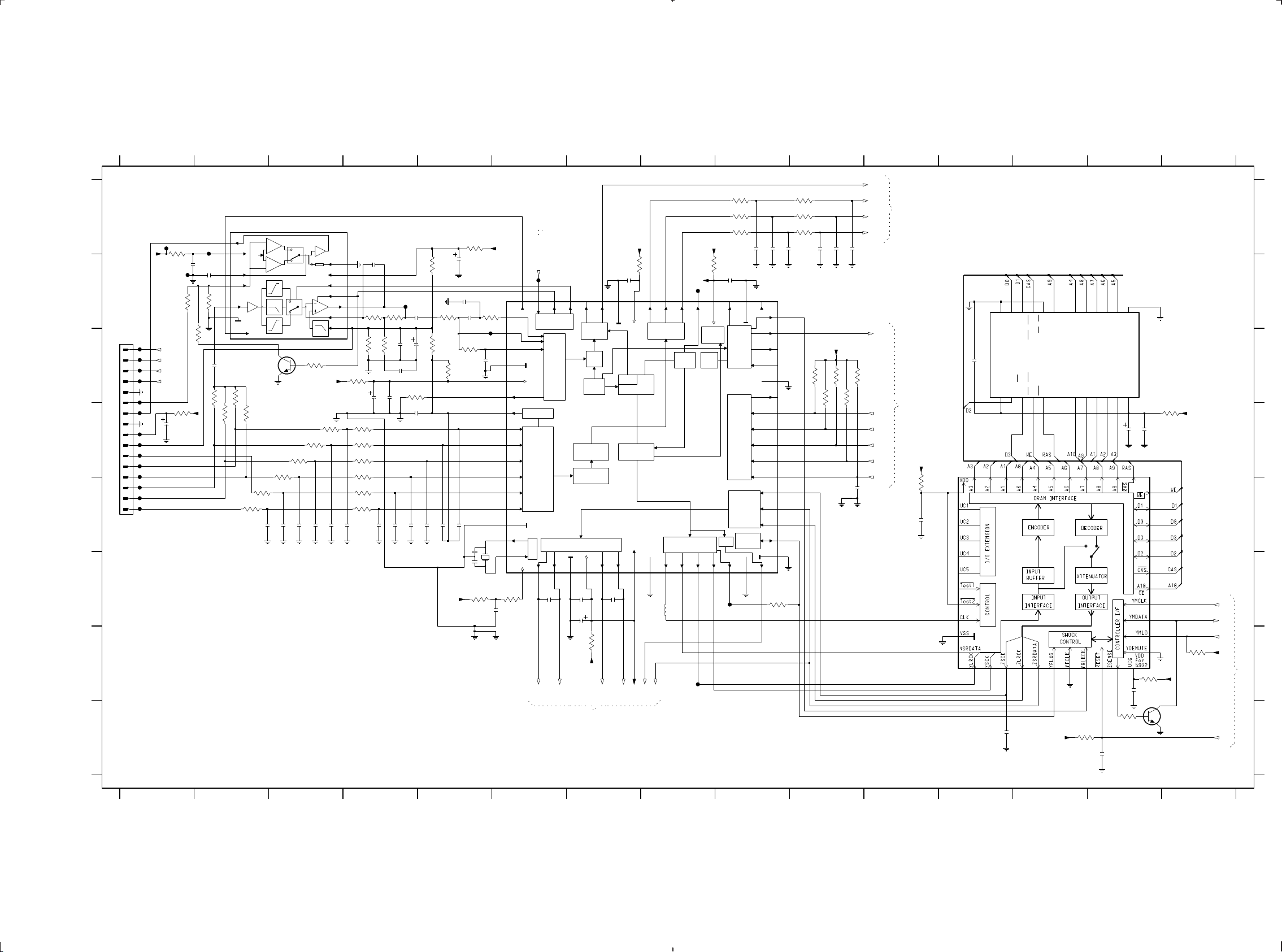
CD PARTD - CIRCUIT DIAGRAM
4-3 4-3
2802 B5
1830 C1
2803 C4
1840 E5
2800 B1
2804 C4
2801 B2
2805 C2
CD-PART
A
B
1830
F830
16
F831
15
C
D
E
F
G
H
F832
14
F833
13
H
12
F834
11
F835
10
H
9
F836
8
F837
7
F838
6
F841
5
F842
4
F839
3
F840
2
F843
1
FMN
2830 D1 2846 B4
2834 E3
2835 E3
2831 E2
2836 E3
2832 E3
2837 E4
2833 E3
2838 E4
2839 E4
2840 E5
2841 E5
2842 E5
2843 C4
2844 C4
2845 D4
2847 B5
2848 B5
2849 C5
2850 A9
2851 A9
2852 A9
2853 A10
2854 A10
2856 E10
2857 F5
2858 F6
2859 F7
2860 F7
2861 B7
2862 B9
2880 E11
2881 H14
2885 D14
2886 D14
2887 C12
2888 F7
2889 H12
2890 B4
2891 C4
3800 A1
1 2 3 4 5 6
7800
+2.6V
F848
Track+
Focus+
FocusTrack-
3800
4R7
F850
3801
2830
22u
H
15K
3830
10R
H
+2.6V
2800
4u7
3809
F849
2801
4n7
56K
TZA1024
LD1
1,8V
VCCL2
2,5V
CFIL3
0,8V
MON4
0,2V
3802
68K
DIN5
0,7V
GND6
0V
PWRON7
2,4V
H
2805
100n
5K6
5K6
3832
5K6
3833
3831
3835
27K
3834
5K6
Vgap
3836
27K
V/I
V/I
1x
4x
2x
3808
220K
7801
BC847BW
H
3839
33K
3838
33K
3837
33K
2833
2832
2831
180p
180p
330p
H
H
H
H
2834
180p
+2.6V
RGADJ 14
VCC2
EQSEL 12
CDRW 11
RFEQO 10
RFFB
CMFB 8
3840
33K
2835
180p
H
0V
H
2890
4p7
13
2,5V
0V
0V
1,4V
0,8V
9
1,3V
H
3847
33R
3841
10K
3842
10K
3843
10K
3844
10K
3845
10K
3846
10K
2836
220p
180p
2837
H
3875
4K7
3806
3K3
2843
22u
H
3805
X
3876
4K7
4K7
2844
100n
H
2891
22p
220p
2838
F851
H
2803
100n
3803
3K3
2846
1n
2804
47u
X
3848
33K
2845
47n
220p
220p
2839
2840
H
H
H
3807
470R
3849
1K
220p
+2.6V
2841
H
3874
1M
2847
22n
2842
220p
22u
2802
2848
3850
3804
47R
27p
22K
CSTCC
8.46MHz
1840
3867
22R
7830
SAA7324
3851
F844
H
1K
1,2V
2849
10n
2,5V
1,2V
1,3V
1,3V
1,3V
1,3V
+2.6V
LDON
1,2V
HFREF1
1,2V
HFIN2
ISLICE3
0V
VSSA14
VDDA15
IREF6
1,3V
VRIN7
1,3V
D18
1,3V
D29
1,3V
D310
D411
R112
R213
0V
VSSA214
CROUT15
CRIN16
1,2V
VDDA2
3868
22R
2857
100n
A
3801 B1
3802 B2
3803 B5
3804 A5
INNERSWITCH
F852
2,4V 2,6V
63
64
V1
VREF GEN.
ADC
TIMING
LN18LP
17
2,6V 1,3V
3805 B4
3806 C4
3807 C5
3808 C3
to CONTROL / SUPPLY-PART
0V 0V
62
V461V5
VERSATILE
INTERFACE
FRONT
END
BITSTREAM DAC
VNEG20VPOS
19
1,3V 0V 2,5V 1,3V
2858
1n5
A
LPLN
to AUDIO-PART
3809 C2
3830 D1
3831 C2
3832 C2
7 8
D
0,4V
0,4V
60
VSSD3
MOTO159MOTO2
MOTOR
CONTROL
DIG.
PLL
EFM
DEMOD
CONTROL
FUNCTION
PRE-
PROCESSING
RN22RP
21
2888
2860
100n
1n5
2859
47u
3869
47R
+2.6V
3833 D2
3834 D2
3835 E2
3836 E2
2.6V-D
3852
10R
2861
1u
0V
2,6V
57
58
VDDD2C
ADDR
SRAM
AUDIO
PROCESSOR
SELPLL
24
23
1,3V 2,5V
E_KILL
RPRN
+Audio
3837 D3
3838 D3
3839 D3
3840 D32882 G14
1,3V
56
SL
OUTPUT
STAGES
TEST1
25
0V
D
KILL
55
FO
CL16
26
5800
100M
3841 D4
3842 D4
3843 D4
3844 D4
+VR
F846
54
RA
ERROR
CORR.
SER. DATA
INTERFACE
DATA
27
F847
3861 C10
3853 B8
3845 E4
3849 B5
3846 E4
3850 C5
3847 C4 F832 C1
3851 B5
3852 B7
3848 C4
3854 A9
3855 A9
3856 A9
3857 A10
3858 A10
3859 A10
3860 C10
3862 C102855 A10
3863 C10
3864 C10
3865 F9
3867 F5
3868 F6
3869 G7
9 10 11
3874 C5
3875 B4
3876 C4
3880 E11
3885 H13
3890 D15
3886 H14
5800 F8
3887 G14
7800 A2
3888 G15
7801 C3
12 13 14 15
DM
2851
3n3
D
SUB 46
RAB 41
SCL 40
SDA 39
SDI
3865
3K3
2852
3n3
3857
2K2
3858
2K2
3859
2K2
2853
1n5
2854
1n5
2855
3n3
Sledge
to CONTROL / SUPPLY-PART
Focus
Radial
D
25
26
D
D
GND | GND
2887
33n
VCC | I/01
2
1
0V 0V 0V 0V
7880
2,6V
1
2,5V
3
2,5V
2,5V
5
2,5V
6
0V
7
2,5V
8
2,6V
1,3V
9
10
0V
1,3V
11
12 13 14 15 16 17 18 19220 21 22
1,3V 1,3V 1,3V
0V
1,5V
3860
10K
3861
2.6V-D
3862
10K
0V
2,1V
0V
D
0V
2,0V
0,3V
1,9V
1,8V
2,6V
1,3V
1,0V
36
1,3V
0,1V
0V
10K
10K
3863
SFSY
3864
10K
SILD
RAB
SCL
SDA
PORES
2856
33n
D
2.6V-D
from/to CONTROL / SUPPLY-PART
3880
22R
2880
100n
D
D
0V1,4V1,2V
53
CFLG
WCLK
28
2.6V-D
EBU
INTERF.
PEAK
DET.
3853
10R
2,6V
52
VDDD1P
KILL
SCLK
29
2862
1u
F845
3854
2K2
3855
2K2
3856
2K2
2850
3n3
D
0V
D
0V
50
51
DOEM
VSSD2
SUBCODE
PROCESSOR
STATUS 43
INTERFACE
MICROCONTROLLER
RESETn 38
SER. DATA
LOOPBACK
INTERF.
VERSAT.
INTERF.
VSSD1 33
TEST2
EF
31
30
D
0V
49
CL11|4
SBSY 48
SFSY 47
RCK 45
TEST3 44
SILD 42
SCLI 37
WCLI 35
V2|V3 34
KILL
32
2,6V
D
7830 B5
7880 D12
7881 C12
7882 H14
23
24
I/04 | I/04
I/03 | I/03
CAS | CAS
WE | RAS
I/02 | WE
I/01 | I/02
345
0V
1,3V 0,9V 0,1V
2889
22p
F830 C1
F834 C1
F831 C1
F835 D1
F836 D1
F833 C1
F837 D1
{A1,A2,A3,A4,A5,A6,A7,A8,A9,A10,D0,D1,D2,D3,A0,RAS,WE,CAS}
22
OE | OE
RAS | A9
0V
18
19
21
A9 | NC
A8 | NC
7881
DRAM_16/4 BIT
16 MBit | 4 MBit
A10 | NC
NC | NC
8
9
6
383944041424344
0V 0V 0V
0V
0V
D
2.6V-D
3885
10K
17
A7 | A8
A0 | A0
2,6V
D
F838 D1
F839 E1
F840 E1
F841 D1
16
A6 | A7
A5 | A6
A1 | A1
A2 | A2
101112
0V
0V
2881
100n
15
A4 | A5
A3 | A3
14
GND | A4
VCC | VCC
13
2886
22u
D
34353637
0V
D
3886
10K
F842 D1
F843 E1
F844 C5
F845 F9
D
3887
22R
2882
100n
2885
100n
33
32
31
30
29
28
27
26
25
24
23
D
3890
22R
2,5V
1,2V
1,3V
1,2V
1,2V
2,5V
2,4V
2,0V
1,8V
2,7V
0V
D
2.6V-D
1,8V
7882
BC847BW
D
F846 B8
F847 G8
F848 A1
F849 A2
2.6V-D
3888
10K
F850 B1
F851 B4
F852 B6
2.6V-D
NPC_RESET
SCL
SDA
YMLD
A
B
C
D
E
F
G
from/to CONTROL / SUPPLY-PART
H
1 2 3
4
5
6 7 8
9 10 11 12
13 14 15
PCS 107 240
Page 22
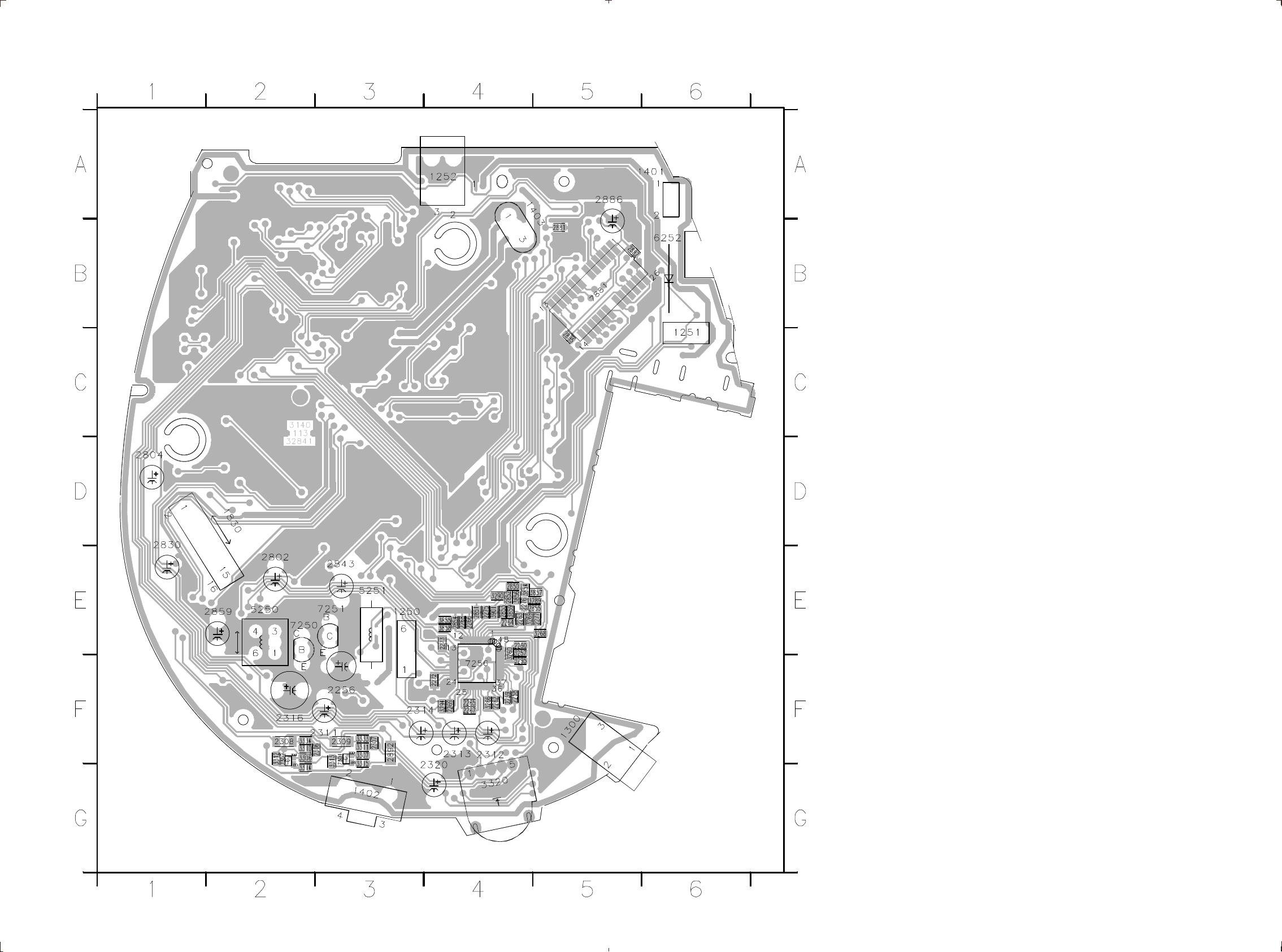
LAYOUT DIAGRAM - COMPONENT SIDE VIEW
4-4 4-4
1250 F4 2802 E1 3313 H3
1251 C8 2804 E1 3314 H3
1252 A5 2830 F1 3315 H4
1300 H6 2843 F4 3320 I5
1401 B8 2850 F6 3322 H6
1402 H4 2851 F5 3323 H6
1403 A6 2852 F6 3324 H6
1830 F2 2853 F5 3325 H6
2256 G3 2854 G5 3333 H4
2258 G6 2855 F6 3334 H3
2259 G6 2859 F2 3704 A7
2260 G6 2881 B6 3708 A7
2262 H5 2885 C6 3854 F6
2263 F6 2886 A7 3855 G5
2264 F6 2887 B7 3856 F6
2265 H5 2892 H4 3857 F6
2266 G5 2893 A7 3858 G5
2267 H5 3257 G6 3859 F6
2268 G5 3260 G6 3901 F5
2269 H5 3265 C5 5250 F2
2270 C5 3266 H5 5251 F4
2272 G5 3268 F6 6252 B7
2273 G5 3269 G6 7250 F3
2274 C5 3272 C5 7251 F4
2275 F5 3273 C5 7256 G5
2276 F6 3274 C5 7300 G2
2277 G6 3275 C5 7301 H4
2278 H6 3276 C5 7302 H3
2300 G2 3277 C5 7701 A7
2301 G2 3278 D5 7881 B7
2302 G2 3289 A7
2303 G2 3290 F5
2304 G2 3294 H5
2305 G2 3295 G6
2306 H3 3300 G2
2307 H4 3301 G2
2308 H3 3302 G2
2309 H3 3303 G2
2311 H3 3304 G2
2312 H5 3305 G2
2313 H5 3306 H3
2314 H4 3307 H4
2316 G3 3308 G2
2320 H5 3309 G2
2322 H6 3310 H3
2323 H6 3311 H4
2702 A7 3312 H3
PCS 107 241
Page 23
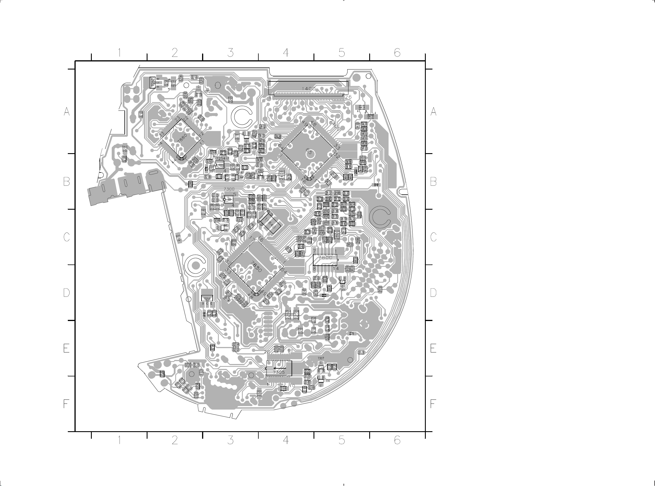
LAYOUT DIAGRAM - COPPER SIDE VIEW
4-5 4-5
1400 A4 2846 C5 3318 F4 3837 B5 7306 E5
1840 C4 2847 C4 3319 E5 3838 B5 7307 E5
2250 D4 2848 C4 3321 E5 3839 B5 7400 A4
2251 A1 2849 C4 3327 E4 3840 C5 7800 C5
2252 D5 2856 D3 3328 E5 3841 C5 7801 D5
2253 D5 2857 B3 3331 B3 3842 B5 7830 C3
2254 E3 2858 C3 3332 C3 3843 B5 7880 A2
2255 E4 2860 C3 3335 E4 3844 B5 7882 A2
2257 D4 2861 D4 3400 A5 3845 B5
2261 A3 2862 D4 3401 A5 3846 B5
2271 A3 2880 B2 3402 A5 3847 D4
2310 C2 2882 A2 3403 A5 3848 C4
2315 E4 2888 C3 3404 A5 3849 C5
2317 E4 2889 A2 3405 A5 3850 C4
2318 F4 2890 D5 3406 A5 3851 C4
2319 F4 2891 D4 3407 A4 3852 D4
2321 F4 3250 D5 3408 A4 3853 D4
2324 E2 3251 A2 3409 A4 3860 D3
2325 E2 3252 E3 3410 A3 3861 D3
2326 E2 3253 A1 3411 B5 3862 D3
2327 E4 3254 A2 3412 B5 3863 D3
2328 E5 3255 A2 3413 B5 3864 D3
2400 B5 3256 E3 3414 A5 3865 C3
2401 B4 3258 B3 3415 B5 3867 B3
2402 A4 3259 B3 3416 B5 3868 C3
2403 A4 3261 A2 3417 B5 3869 C3
2404 A4 3263 B3 3418 A5 3874 C4
2405 B4 3264 A3 3419 A5 3875 D5
2701 B4 3267 B3 3420 B5 3876 D5
2800 C5 3270 D3 3701 B4 3880 A2
2801 C5 3271 D3 3800 C5 3885 A2
2803 C5 3279 B2 3801 C5 3886 A2
2805 B5 3280 B2 3802 C5 3887 A2
2831 B5 3281 B3 3803 C5 3888 A2
2832 B5 3282 B3 3804 D6 3890 A2
2833 B5 3283 B3 3805 D5 5800 C3
2834 B5 3284 C2 3806 C5 6251 A2
2835 B5 3285 B4 3807 C5 6400 A6
2836 C5 3286 B4 3808 D5 6401 A5
2837 B5 3287 A3 3809 C5 7252 A2
2838 B5 3288 D5 3830 D6 7254 B3
2839 B5 3291 A1 3831 C5 7255 D3
2840 B5 3292 B6 3832 C5 7258 A3
2841 C4 3293 D3 3833 B5 7259 B3
2842 C5 3296 B3 3834 B5 7260 B3
2844 C4 3316 B3 3835 B5 7303 B3
2845 C5 3317 D3 3836 B5 7305 E4
PCS 107 242
Page 24
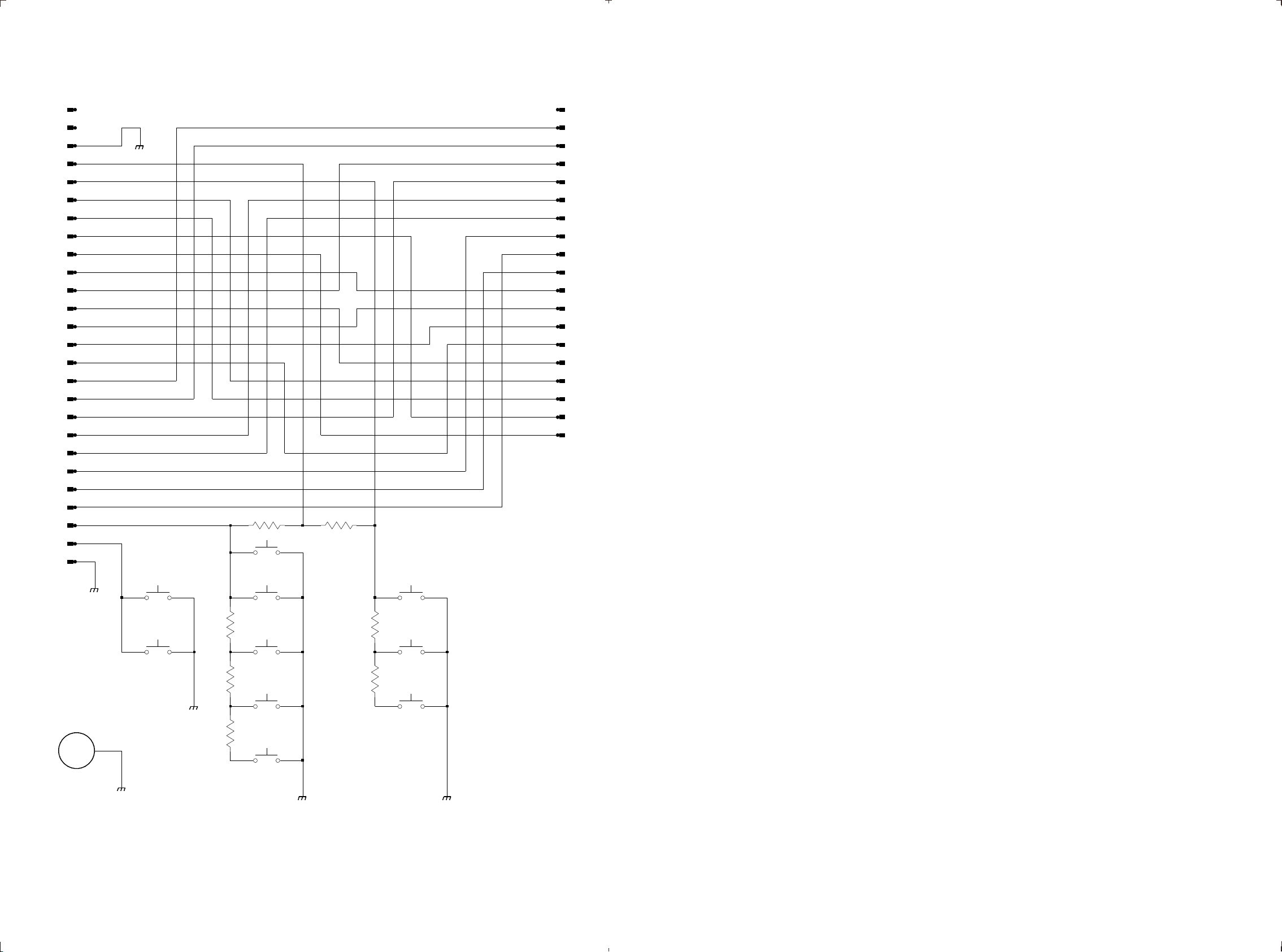
MEMBRANE ASSEMBLY
NC
26
NC
25
ESD-GND
24
+2.6V
23
KEY1
22
C0
21
C1
20
C2
19
C3
18
S13
17
S12
16
S11
15
S10
14
S9
13
S8
12
S7
11
S6
10
S5
9
S4
8
S3
7
S2
6
S1
5
S0
4
KEY2
3
PLAY
2
ESD-GND
1
4-6 4-6
MECHANICAL PARTSLIST
401 3140 114 37310 Decorative Cover
NC
S12
S13
S10
S11
S7
S6
S5
S4
S3
S2
S0
S1
S9
S8
C0
C1
C2
C3
19
18
17
16
15
14
13
12
11
10
9
8
7
6
5
4
3
2
1
402 3140 114 37400 Door-ACT-DA23
403 4822 401 11793 Metal Clip Door
404 3140 117 60660 Menbrane LCD Assy
406 4822 466 12154 Plate Door
407 4822 532 13114 O Ring Door
408 3140 114 36610 Cabinet-DA23
409 3103 309 05340 CD DA23L Drive Assy
411 4822 463 11241 Slider Resume
412 3140 117 60640 Bottam-DA23 Assy (For -/00/01)
412 3140 117 60650 Bottam-DA23 Assy (For -/17)
413 4822 401 11794 Metal Clip
414 4822 401 11792 Clip
416 4822 417 11402 Hinge Assy
417 3140 114 36620 Door Battery
418 4822 492 11525 Spring Battery Short
419 3103 304 69590 Suspension
421 4822 492 11517 Spring Battery Minus
422 4822 492 11516 Spring Battery Plus
423 3103 301 45430 Spring Battery Charge
424 4822 402 11253 Bracket Clip
426 3140 114 37320 Belt Clip
3140 115 28100 Instruction Manual (For -/00/01)
3140 115 28110 Instruction Manual (For -/00)
3140 115 28120 Instruction Manual (For -/17)
Note:Only these parts mentioned in the list are
normal service parts.
CONTACT AREA X
PCS 107 243
Page 25
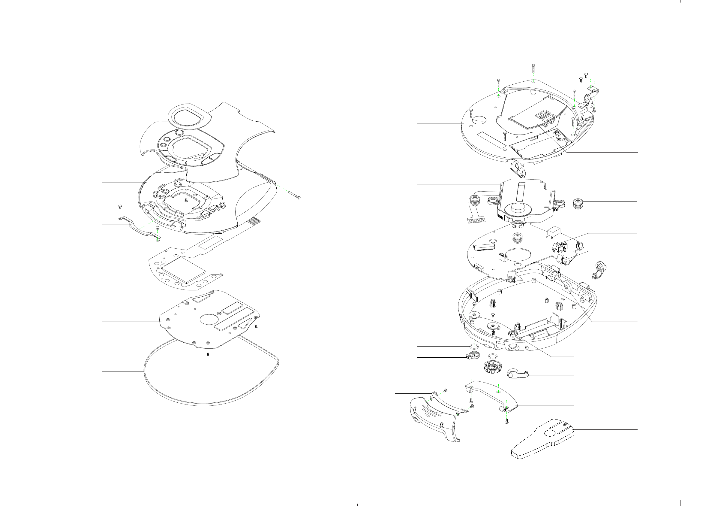
EXPLODED VIEW DIAGRAM
5-1 5-1
SCREWS LIST
1 C M1.3 x 2.5
2 C M1.5 x 3
3 C M1.5 x 4.5
4 C M1.6 x 9
5 C M1.6 x 15
401
402
403
2 (2x)
501
5 (2x)
4 (6x)
3 (4x)
416
408
417
418
409
419
421
404
406
407
1 (7x)
413
414
411
412a
412b
412c
412d
412e
2 (2x)
422
412f
2
2
423
412g
412h
424
3 (3x)
426
PCS 107 244
Page 26

ELECTRICAL PARTSLIST
6-1 6-1
ELECTRICAL PARTSLIST
- CAPACITORS - - CAPACITORS -
2250 4822 126 14083 4µ7 10V 2321 4822 126 14472 1µF 10% X7R 10V
2251 4822 126 14472 1µF 10% X7R 10V 2322 4822 126 14305 100nF 10% X7R 16V
2252 4822 126 14241 330pF NPO 50V 2323 4822 126 14305 100nF 10% X7R 16V
2253 4822 126 14494 22nF 10% X7R 25V 2324 4822 126 14549 33nF 16V X7R
2254 4822 126 13193 4,7nF 10% X7R 63V 2325 4822 126 14549 33nF 16V X7R
2255 4822 126 14472 1µF 10% X7R 10V 2326 5322 126 11583 10nF 10% X7R 50V
2256 4822 124 12248 100µF 20% 4V 2327 4822 126 14305 100nF 10% X7R 16V
2257 4822 126 14083 4µ7 10V 2328 4822 126 14305 100nF 10% X7R 16V
2258 3198 017 41050 1µF Y5V 10V 2400 4822 126 14472 1µF 10% X7R 10V
2259 5322 126 11583 10nF 10% X7R 50V 2401 4822 126 14083 4µ7 10V
2260 4822 122 31765 100pF 2% NP0 63V 2402 4822 126 14305 100nF 10% X7R 16V
2261 4822 126 14305 100nF 10% X7R 16V 2403 4822 126 14305 100nF 10% X7R 16V
2262 5322 126 11579 3,3nF10% X7R 63V 2404 4822 126 14305 100nF 10% X7R 16V
2263 4822 126 13883 220pF 5% 50V 2405 4822 126 14305 100nF 10% X7R 16V
2264 4822 126 13883 220pF 5% 50V 2701 5322 126 11578 1nF 10% X7R 50V
2265 4822 126 14305 100nF 10% X7R 16V 2702 5322 126 11583 10nF 10% X7R 50V
2266 4822 126 13883 220pF 5% 50V 2800 4822 126 14083 4µ7 10V
2267 4822 126 14305 100nF 10% X7R 16V 2801 4822 126 13193 4,7nF 10% X7R 63V
2268 4822 126 13883 220pF 5% 50V 2802 4822 124 40998 22µF 20% 6,3V
2269 4822 126 14305 100NF 10% X7R 16V 2803 4822 126 14305 100nF 10% X7R 16V
2270 4822 126 13881 470pF 5% 50V 2804 4822 124 12362 47µF 20% 4V
2271 4822 126 14472 1µF 10% X7R 10V 2805 4822 126 14305 100nF 10% X7R 16V
2272 4822 126 14472 1µF 10% X7R 10V 2830 4822 124 40998 22µF 20% 6,3V
2273 4822 126 14472 1µF 10% X7R 10V 2831 4822 126 14508 180pF 5% 50V NP0
2274 5322 126 11578 1nF 10% X7R 50V 2832 4822 126 14241 330pF NPO 50V
2275 5322 126 11583 10nF 10% X7R 50V 2833 4822 126 14508 180pF 5% 50V NP0
2276 4822 126 14305 100nF 10% X7R 16V 2834 4822 126 14508 180pF 5% 50V NP0
2277 3198 017 41050 1µF Y5V 10V 2835 4822 126 14508 180pF 5% 50V NP0
2278 3198 017 41050 1µF Y5V 10V 2836 4822 126 14508 180pF 5% 50V NP0
2300 4822 126 13883 220pF 5% 50V 2837 4822 126 13883 220pF 5% 50V
2301 4822 126 13883 220pF 5% 50V 2838 4822 126 13883 220pF 5% 50V
2302 4822 122 31765 100pF 2% NP0 63V 2839 4822 126 13883 220pF 5% 50V
2303 4822 122 31765 100pF 2% NP0 63V 2840 4822 126 13883 220pF 5% 50V
2304 4822 126 13883 220pF 5% 50V 2841 4822 126 13883 220pF 5% 50V
2305 4822 126 13883 220pF 5% 50V 2842 4822 126 13883 220pF 5% 50V
2306 5322 126 11579 3,3nF 10% X7R 63V 2843 4822 124 40998 22µF 20% 6,3V
2307 5322 126 11579 3,3nF 10% X7R 63V 2844 4822 126 14305 100nF 10% X7R 16V
2308 4822 126 14083 4µ7 10V 2845 3198 017 34730 47nF X7R 16V
2309 4822 126 14083 4µ7 10V 2846 5322 126 11578 1nF 10% X7R 50V
2310 4822 126 14472 1µF 10% X7R 10V 2847 4822 126 14494 22nF 10% X7R 25V
2311 4822 124 40998 22µF 20% 6,3V 2848 4822 126 11669 27pF
2312 4822 124 22652 2,2µF 20% 50V 2849 5322 126 11583 10nF 10% X7R 50V
2313 4822 124 22651 1,0µF 20% 50V 2850 5322 126 11579 3,3nF 10% X7R 63V
2314 4822 124 40998 22µF 20% 6,3V 2851 5322 126 11579 3,3nF 10% X7R 63V
2315 4822 126 14305 100nF 10% X7R 16V 2852 5322 126 11579 3,3nF 10% X7R 63V
2316 4822 124 12052 220µF 20% 6,3V 2853 4822 126 14247 1,5nF X7R 50V
2317 4822 126 14305 100nF 10% X7R 16V 2854 4822 126 14247 1,5nF X7R 50V
2318 4822 126 14472 1µF 10% X7R 10V 2855 5322 126 11579 3,3nF 10% X7R 63V
2319 3198 017 41050 1µF Y5V 10V 2856 4822 126 14549 33nF 16V X7R
2320 4822 124 22652 2,2µF 20% 50V 2857 4822 126 14305 100nF 10% X7R 16V
- CAPACITORS - - RESISTORS -
2858 4822 126 13344 1,5nF 5% 63V 3281 4822 117 12925 47K 1% 0.063W
2859 4822 124 12362 47µF 20% 4V 3282 4822 051 30474 470K 5% 0,062W
2860 4822 126 13344 1,5nF 5% 63V 3283 4822 051 30474 470K 5% 0,062W
2861 3198 017 41050 1µF Y5V 10V 3284 4822 116 30467 10K 5%
2862 3198 017 41050 1µF Y5V 10V 3286 4822 051 30103 10K 5% 0,062W
2880 4822 126 14305 100nF 10% X7R 16V 3287 4822 051 30103 10K 5% 0,062W
2881 4822 126 14305 100nF 10% X7R 16V 3288 4822 051 30109 10R 5% 0,062W
2882 4822 126 14305 100nF 10% X7R 16V 3289 4822 051 30562 5K6 5% 0,063W
2885 4822 126 14305 100nF 10% X7R 16V 3291 4822 117 13632 100K 1% 0.62W
2886 4822 124 40998 22µF 20% 6,3V 3292 4822 051 30103 10K 5% 0,062W
2887 4822 126 14549 33nF 16V X7R 3293 4822 051 30331 330R 5% 0,062W
2888 5322 126 11583 10nF 10% X7R 50V 3294 4822 051 30474 470K 5% 0,062W
2889 4822 122 33761 22pF 5% NP0 50V 3295 4822 117 12889 270K 1% 0,063W
2892 4822 126 14083 4µ7 10V 3300 4822 051 30333 33K 5% 0,062W
3301 4822 051 30333 33K 5% 0,062W
- RESISTORS -
3302 4822 051 30333 33K 5% 0,062W
3250 4822 051 30681 680R 5% 0,062W 3303 4822 051 30333 33K 5% 0,062W
3251 4822 051 30271 270R 5% 0,062W 3304 4822 051 30153 15K 5% 0,062W
3252 4822 051 30331 330R 5% 0,062W 3305 4822 051 30153 15K 5% 0,062W
3253 4822 051 30271 270R 5% 0,062W 3306 4822 051 30222 2K2 5% 0,062W
3254 4822 051 30103 10K 5% 0,062W
3307 4822 051 30222 2K2 5% 0,062W
3255 4822 117 12925 47K 1% 0.063W 3308 4822 051 30153 15K 5% 0,062W
3256 4822 051 30272 2K7 5% 0,062W 3309 4822 051 30153 15K 5% 0,062W
3257 4822 117 12891 220K 1% 3310 4822 051 30562 5K6 5% 0,063W
3258 5322 117 13019 100K 1% 0.063W 3311 4822 051 30562 5K6 5% 0,063W
3259 5322 117 13035 68K 1% 0.063W
3312 4822 051 30105 1M 5% 0,062W
3260 4822 051 30105 1M 5% 0,062W 3313 4822 051 30105 1M 5% 0,062W
3261 4822 051 30103 10K 5% 0,062W 3314 4822 051 30332 3K3 5% 0,062W
3263 4822 051 30223 22K 5% 0,062W 3315 4822 051 30332 3K3 5% 0,062W
3264 5322 117 13019 100K 1% 0.063W 3316 4822 051 30103 10K 5% 0,062W
3265 4822 051 30334 330K 5% 0,062W
3317 4822 051 30472 4K7 5% 0,062W
3266 4822 051 30103 10K 5% 0,062W 3318 4822 117 13632 100K 1% 0.62W
3267 5322 117 13035 68K 1% 0.063W 3319 4822 117 13613 2R2 5%
3268 4822 117 12706 10K 1% 0.063W 3320 4822 101 11936 Var Resistor 10K
3269 4822 117 12706 10K 1% 0.063W 3321 4822 051 30103 10K 5% 0,062W
3270 2322 702 70278 2R7 5%
3322 2322 702 60688 6R8 5% 0.062W
3271 2322 702 70278 2R7 5% 3323 2322 702 60688 6R8 5% 0.062W
3272 4822 051 30472 4K7 5% 0,062W 3324 4822 117 13613 2R2 5%
3273 4822 117 13632 100K 1% 0.62W 3325 4822 117 13613 2R2 5%
3274 4822 117 13632 100K 1% 0.62W 3327 4822 051 30105 1M 5% 0,062W
3275 4822 051 30334 330K 5% 0,062W
3328 4822 117 12925 47K 1% 0.063W
3276 4822 051 30183 18K 5% 0,062W 3333 4822 051 30183 18K 5% 0,062W
3277 4822 051 30183 18K 5% 0,062W 3334 4822 051 30183 18K 5% 0,062W
3278 4822 051 30103 10K 5% 0,062W 3335 4822 051 30472 4K7 5% 0,062W
3279 3198 021 32250 2M2 5% 3400 4822 117 13632 100K 1% 0.62W
3280 4822 051 30474 470K 5% 0,062W
3401 4822 117 12891 220K 1%
3402 4822 117 12891 220K 1%
3403 4822 117 12891 220K 1%
3404 4822 051 30102 1K 5% 0,062W
3405 4822 051 30102 1K 5% 0,062W
PCS 107 245
Page 27

6-2
ELECTRICAL PARTSLIST
- RESISTORS - - RESISTORS -
3406 4822 051 30102 1K 5% 0,062W 3853 4822 051 30109 10R 5% 0,062W
3407 4822 051 30154 150K 5% 0,062W 3854 4822 051 30222 2K2 5% 0,062W
3408 4822 051 30123 12K 5% 0,062W 3855 4822 051 30222 2K2 5% 0,062W
3409 4822 051 30562 5K6 5% 0,063W 3856 4822 051 30222 2K2 5% 0,062W
3410 4822 051 30109 10R 5% 0,062W 3857 4822 051 30222 2K2 5% 0,062W
3411 4822 051 30109 10R 5% 0,062W 3858 4822 051 30222 2K2 5% 0,062W
3412 4822 051 30101 100R 5% 0,062W 3859 4822 051 30222 2K2 5% 0,062W
3413 4822 051 30101 100R 5% 0,062W 3860 4822 051 30103 10K 5% 0,062W
3414 4822 117 12925 47K 1% 0.063W 3861 4822 051 30103 10K 5% 0,062W
3415 4822 051 30103 10K 5% 0,062W 3862 4822 051 30103 10K 5% 0,062W
3416 4822 051 30472 4K7 5% 0,062W 3863 4822 051 30103 10K 5% 0,062W
3417 4822 051 30103 10K 5% 0,062W 3864 4822 051 30103 10K 5% 0,062W
3419 4822 051 30008 Jumper 3865 4822 051 30332 3K3 5% 0,062W
3420 4822 051 30272 2K7 5% 0,062W 3867 4822 117 12139 22R 5% 0,062W
3701 4822 117 13632 100K 1% 0.62W 3868 4822 117 12139 22R 5% 0,062W
3704 4822 051 30105 1M 5% 0,062W 3869 4822 051 30471 470R 5% 0,062W
3708 4822 051 30103 10K 5% 0,062W 3874 4822 051 30105 1M 5% 0,062W
3800 4822 117 13608 4,7R 5% 0,0016W 3875 4822 051 30472 4K7 5% 0,062W
3801 4822 051 30153 15K 5% 0,062W 3880 4822 117 12139 22R 5% 0,062W
3802 4822 051 30683 68K 5% 0,062W 3885 4822 051 30103 10K 5% 0,062W
3803 4822 051 30332 3K3 5% 0,062W 3886 4822 051 30103 10K 5% 0,062W
3804 4822 051 30479 47R 5% 0,062W 3887 4822 117 12139 22R 5% 0,062W
3805 4822 051 30472 4K7 5% 0,062W 3888 4822 051 30103 10K 5% 0,062W
3806 4822 051 30332 3K3 5% 0,062W 3890 4822 117 12139 22R 5% 0,062W
3807 4822 051 30471 470R 5% 0,062W 3901 4822 051 30103 10K 5% 0,062W
3808 4822 117 12891 220K 1% 4201 4822 051 30008 Jumper
3809 4822 051 30563 56K 5% 0,062W
3830 4822 051 30109 10R 5% 0,062W - COIL & FILTER -
3831 4822 051 30562 5K6 5% 0,063W
3832 4822 051 30562 5K6 5% 0,063W 5251 4822 157 51462 Coil 10µH 10%
5800 4822 157 11781 Filter BLM11A601SPT1
3833 4822 051 30562 5K6 5% 0,063W
3834 4822 051 30562 5K6 5% 0,063W - DIODES -
3835 4822 051 30273 27K 5% 0,062W
3836 4822 051 30273 27K 5% 0,062W 6251 4822 130 10654 Diode BAT254
3837 4822 051 30333 33K 5% 0,062W 6252 5322 130 81917 Diode SB140
6400 4822 130 83757 Diode BAS216
3838 4822 051 30333 33K 5% 0,062W 6401 4822 130 10654 Diode BAT254
3839 4822 051 30333 33K 5% 0,062W
3840 4822 051 30333 33K 5% 0,062W - IC & TRANSISTORS -
3841 4822 051 30103 10K 5% 0,062W
3842 4822 051 30103 10K 5% 0,062W 7250 9322 003 64676 Trans TBC337-40
7251 5322 130 44647 Trans BC368
3843 4822 051 30103 10K 5% 0,062W 7252 4822 130 60142 Trans BC869
3844 4822 051 30103 10K 5% 0,062W 7254 9322 142 72685 IC SM TC75W51FU
3845 4822 051 30103 10K 5% 0,062W 7255 5322 130 61569 Trans BC868
3846 4822 051 30103 10K 5% 0,062W
3847 4822 051 30339 33R 5% 0,062W 7256 9322 160 31669 IC SC111259FTA
7258 3198 010 42310 Trans BC847BW
3848 4822 051 30333 33K 5% 0,062W 7259 5322 130 42756 Trans BC857C
3849 4822 051 30102 1K 5% 0,062W 7260 3198 010 42310 Trans BC847BW
3850 4822 051 30223 22K 5% 0,062W 7300 9322 142 72685 IC SM TC75W51FU
3851 4822 051 30102 1K 5% 0,062W
3852 4822 051 30109 10R 5% 0,062W
PCS 107 246
Page 28

6-3
ELECTRICAL PARTSLIST
- IC & TRANSISTORS -
7301 3198 010 42310 Trans BC847BW
7302 3198 010 42310 Trans BC847BW
7303 3198 010 42310 Trans BC847BW
7305 4822 209 16083 IC BA3574BFS
7306 3198 010 42310 Trans BC847BW
7307 3198 010 42310 Trans BC847BW
7400 8203 303 11110 IC SM TMP86C8296-UP
7701 3198 010 42310 Trans BC847BW
7800 4822 209 17286 IC TZA1024T/N1
7801 3198 010 42310 Trans BC847BW
7830 9352 641 80557 IC SAA7324H/M2B
7880 9322 142 87671 IC SM SM5903BF
7881 9322 138 26668 IC SM MSM51V17405D-60TS-K
7882 3198 010 42310 Trans BC847BW
-MISCELLANEOUS -
1250 2422 025 12272 Connector 6P
1251 2422 086 10946 Fuse Rad 630mA 65V
1252 2422 026 05086 DC Jack
1300 2422 026 05085 Headphone Jack
1400 2422 025 16707 Connector 26P
1401 4822 276 12889 Push Switch
1402 4822 277 21643 Slide Switch
1403 2422 540 98516 Filter 4MHz CSTS MG03
1830 4822 267 11028 Connector 16P
1840 4822 242 81546 Filter CSTCS8,46MT-TC
5250 2422 536 00141 Transformer 40µH
Note: Only these parts mentioned in the list are
normal service parts.
PCS 107 247
 Loading...