

Philips A723CN, A723CD Datasheet
Philips Semiconductors Product specification
µA723/723CPrecision voltage regulator
1
1994 Aug 31 853-1063 13721
DESCRIPTION
The µA723/µA723C is a monolithic precision voltage regulator
capable of operation in positive or negative supplies as a series,
shunt, switching, or floating regulator. The 723 contains a
temperature-compensated reference amplifier, error amplifier, series
pass transistor, and current limiter, with access to remote shutdown.
FEATURES
•Positive or negative supply operation
•Series, shunt, switching, or floating operation
•0.01% line and load regulation
•Output voltage adjustable from 2V to 37V
•Output current to 150mA without external pass transistor
•µA723 MIL-STD-883A, B, C available
PIN CONFIGURATION
D,F, N Packages
1
2
3
4
5
6
7 8
14
13
12
11
10
9
NC
CURRENT LIMIT
CURRENT SENSE
INVERTING INPUT
NON-INVERTING INPUT
V–
V
REF
NC
FREQUENCY COMPENS.
NC
V+
V
C
V
OUT
V
Z
SL00503
Figure 1. Pin Configuration
ORDERING INFORMATION
DESCRIPTION TEMPERATURE RANGE ORDER CODE DWG #
14-Pin Ceramic Dual In-Line Package (CERDIP) -55°C to 125°C µA723F 0581B
14-Pin Plastic Dual In-Line Package (DIP) 0 to 70°C µA723CN SOT27-1
14-Pin Plastic Small Outline (SO) Package 0 to 70°C µA723CD SOT108-1
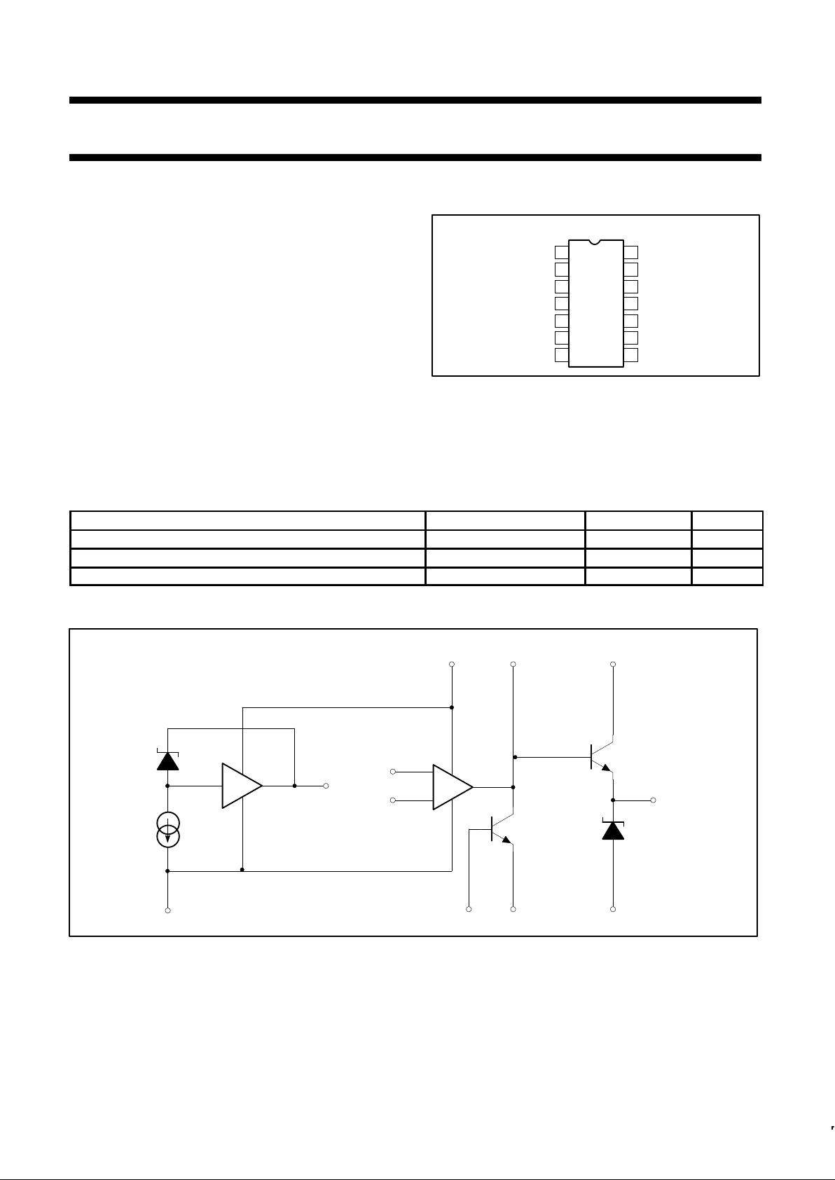
EQUIVALENT CIRCUIT
TEMPERATURE
COMPENSATED
ZENER
7
V–
VOLTAGE
REFERENCE
AMPLIFIER
INVERTING
INPUT
4
ERROR AMP
NON INVERTING
INPUT
–
+
CURRENT
LIMIT
2
3
CURRENT
SENSE
FREQUENCY
COMPENSATION
V+
12
13 11
SERIES PASS
TRANSISTOR
10
9
V
C
V
Z
V
OUT
8
V
REF
V
IN
SL00504
Figure 2. Equivalent Circuit

Philips Semiconductors Product specification
µA723/723CPrecision voltage regulator
1994 Aug 31
2
ABSOLUTE MAXIMUM RATINGS
SYMBOL PARAMETER RATING UNIT
Pulse voltage from V+ to V- (50ms) 50 V
Continuous voltage from V+ to V- 40 V
Input-output voltage differential 40 V
V
DIFF
Error amplifier maximum input differential voltage ±5 V
V
CM
Error amplifier non-inverting input (Pin 5) to -V (Pin 7) 8 V
I
OUT
Maximum output current 150 mA
Current from V
REF
15 mA
Current from V
Z
25 mA
P
MAX
Maximum power dissipation TA=25°C (still-air)
1
F package 1190 mW
N package 1420 mW
D package 1040 mW
T
A
Operating ambient temperature range
µA723
µA723C
-55 to +125
0 to 70
°C
°C
T
STG
Storage temperature range -65 to +150 °C
T
SOLD
Lead soldering temperature (10sec max) 300 °C
NOTES:
1. The following derating factors should be applied above 25°C
F package at 9.5mW/°C
N package at 11.4mW/°C
D package at 8.3mW/°C
 Loading...