

Philips 87LPC768 Datasheet

INTEGRATED CIRCUITS
87LPC768
Low power, low price, low pin count
(20 pin) microcontroller with 4 kB OTP
8-bit A/D,and Pulse Width Modulator
Preliminary specification 2000 May 02

Philips Semiconductors Preliminary specification
Low power, low price, low pin count (20 pin) microcontroller
with 4 kB OTP 8-bit A/D, Pulse Width Modulator
GENERAL DESCRIPTION 1. . . . . . . . . . . . . . . . . . . . . . . . . . . . . . . . . . . . . . . . . . . . . . . . . . . . . . . . . . . . . . . . . . . . . . . . . . . . . . . .
FEATURES 1. . . . . . . . . . . . . . . . . . . . . . . . . . . . . . . . . . . . . . . . . . . . . . . . . . . . . . . . . . . . . . . . . . . . . . . . . . . . . . . . . . . . . . . . . . . . .
ORDERING INFORMATION 2. . . . . . . . . . . . . . . . . . . . . . . . . . . . . . . . . . . . . . . . . . . . . . . . . . . . . . . . . . . . . . . . . . . . . . . . . . . . . . .
PIN CONFIGURATION, 20-PIN DIP AND SO PACKAGES 2. . . . . . . . . . . . . . . . . . . . . . . . . . . . . . . . . . . . . . . . . . . . . . . . . . . .
LOGIC SYMBOL 2. . . . . . . . . . . . . . . . . . . . . . . . . . . . . . . . . . . . . . . . . . . . . . . . . . . . . . . . . . . . . . . . . . . . . . . . . . . . . . . . . . . . . . . . .
BLOCK DIAGRAM 3. . . . . . . . . . . . . . . . . . . . . . . . . . . . . . . . . . . . . . . . . . . . . . . . . . . . . . . . . . . . . . . . . . . . . . . . . . . . . . . . . . . . . . .
PIN DESCRIPTIONS 5. . . . . . . . . . . . . . . . . . . . . . . . . . . . . . . . . . . . . . . . . . . . . . . . . . . . . . . . . . . . . . . . . . . . . . . . . . . . . . . . . . . . .
FUNCTIONAL DESCRIPTION 9. . . . . . . . . . . . . . . . . . . . . . . . . . . . . . . . . . . . . . . . . . . . . . . . . . . . . . . . . . . . . . . . . . . . . . . . . . . . .
Enhanced CPU 9. . . . . . . . . . . . . . . . . . . . . . . . . . . . . . . . . . . . . . . . . . . . . . . . . . . . . . . . . . . . . . . . . . . . . . . . . . . . . . . . . . . . . . . .
Analog Functions 9. . . . . . . . . . . . . . . . . . . . . . . . . . . . . . . . . . . . . . . . . . . . . . . . . . . . . . . . . . . . . . . . . . . . . . . . . . . . . . . . . . . . . .
Analog to Digital Converter 9. . . . . . . . . . . . . . . . . . . . . . . . . . . . . . . . . . . . . . . . . . . . . . . . . . . . . . . . . . . . . . . . . . . . . . . . . . . . . .
A/D Timing 10. . . . . . . . . . . . . . . . . . . . . . . . . . . . . . . . . . . . . . . . . . . . . . . . . . . . . . . . . . . . . . . . . . . . . . . . . . . . . . . . . . . . . . . . . . . .
The A/D in Power Down and Idle Modes 11. . . . . . . . . . . . . . . . . . . . . . . . . . . . . . . . . . . . . . . . . . . . . . . . . . . . . . . . . . . . . . . . . .
Code Examples for the A/D 12. . . . . . . . . . . . . . . . . . . . . . . . . . . . . . . . . . . . . . . . . . . . . . . . . . . . . . . . . . . . . . . . . . . . . . . . . . . . .
Analog Comparators 13. . . . . . . . . . . . . . . . . . . . . . . . . . . . . . . . . . . . . . . . . . . . . . . . . . . . . . . . . . . . . . . . . . . . . . . . . . . . . . . . . . .
I2C Serial Interface 20. . . . . . . . . . . . . . . . . . . . . . . . . . . . . . . . . . . . . . . . . . . . . . . . . . . . . . . . . . . . . . . . . . . . . . . . . . . . . . . . . . . .
Interrupts 24. . . . . . . . . . . . . . . . . . . . . . . . . . . . . . . . . . . . . . . . . . . . . . . . . . . . . . . . . . . . . . . . . . . . . . . . . . . . . . . . . . . . . . . . . . . . .
I/O Ports 26. . . . . . . . . . . . . . . . . . . . . . . . . . . . . . . . . . . . . . . . . . . . . . . . . . . . . . . . . . . . . . . . . . . . . . . . . . . . . . . . . . . . . . . . . . . . . .
Keyboard Interrupt (KBI) 28. . . . . . . . . . . . . . . . . . . . . . . . . . . . . . . . . . . . . . . . . . . . . . . . . . . . . . . . . . . . . . . . . . . . . . . . . . . . . . . .
Oscillator 30. . . . . . . . . . . . . . . . . . . . . . . . . . . . . . . . . . . . . . . . . . . . . . . . . . . . . . . . . . . . . . . . . . . . . . . . . . . . . . . . . . . . . . . . . . . . .
Power Monitoring Functions 32. . . . . . . . . . . . . . . . . . . . . . . . . . . . . . . . . . . . . . . . . . . . . . . . . . . . . . . . . . . . . . . . . . . . . . . . . . . . .
Power Reduction Modes 33. . . . . . . . . . . . . . . . . . . . . . . . . . . . . . . . . . . . . . . . . . . . . . . . . . . . . . . . . . . . . . . . . . . . . . . . . . . . . . . .
Reset 35. . . . . . . . . . . . . . . . . . . . . . . . . . . . . . . . . . . . . . . . . . . . . . . . . . . . . . . . . . . . . . . . . . . . . . . . . . . . . . . . . . . . . . . . . . . . . . . .
Timer/Counters 36. . . . . . . . . . . . . . . . . . . . . . . . . . . . . . . . . . . . . . . . . . . . . . . . . . . . . . . . . . . . . . . . . . . . . . . . . . . . . . . . . . . . . . . .
UART 39. . . . . . . . . . . . . . . . . . . . . . . . . . . . . . . . . . . . . . . . . . . . . . . . . . . . . . . . . . . . . . . . . . . . . . . . . . . . . . . . . . . . . . . . . . . . . . . .
Watchdog Timer 49. . . . . . . . . . . . . . . . . . . . . . . . . . . . . . . . . . . . . . . . . . . . . . . . . . . . . . . . . . . . . . . . . . . . . . . . . . . . . . . . . . . . . . .
Additional Features 51. . . . . . . . . . . . . . . . . . . . . . . . . . . . . . . . . . . . . . . . . . . . . . . . . . . . . . . . . . . . . . . . . . . . . . . . . . . . . . . . . . . .
EPROM Characteristics 52. . . . . . . . . . . . . . . . . . . . . . . . . . . . . . . . . . . . . . . . . . . . . . . . . . . . . . . . . . . . . . . . . . . . . . . . . . . . . . . .
ABSOLUTE MAXIMUM RATINGS 53. . . . . . . . . . . . . . . . . . . . . . . . . . . . . . . . . . . . . . . . . . . . . . . . . . . . . . . . . . . . . . . . . . . . . . . . .
DC ELECTRICAL CHARACTERISTICS 54. . . . . . . . . . . . . . . . . . . . . . . . . . . . . . . . . . . . . . . . . . . . . . . . . . . . . . . . . . . . . . . . . . . .
COMPARATOR ELECTRICAL CHARACTERISTICS 55. . . . . . . . . . . . . . . . . . . . . . . . . . . . . . . . . . . . . . . . . . . . . . . . . . . . . . . . .
A/D CONVERTER DC ELECTRICAL CHARACTERISTICS 55. . . . . . . . . . . . . . . . . . . . . . . . . . . . . . . . . . . . . . . . . . . . . . . . . . .
AC ELECTRICAL CHARACTERISTICS 57. . . . . . . . . . . . . . . . . . . . . . . . . . . . . . . . . . . . . . . . . . . . . . . . . . . . . . . . . . . . . . . . . . . .
87LPC768
2000 May 02
i

Philips Semiconductors Preliminary specification
Low power, low price, low pin count (20 pin) microcontroller with 4 kB
OTP 8-bit A/D, Pulse Width Modulator
GENERAL DESCRIPTION
The 87LPC768 is a 20-pin single-chip microcontroller designed for
low pin count applications demanding high-integration, low cost
solutions over a wide range of performance requirements. A
member of the Philips low pin count family, the 87LPC768 of fers
programmable oscillator configurations for high and low speed
crystals or RC operation, wide operating voltage range,
programmable port output configurations, selectable Schmitt trigger
inputs, LED drive outputs, and a built-in watchdog timer. The
87LPC768 is based on an accelerated 80C51 processor
architecture that executes instructions at twice the rate of standard
80C51 devices.
FEA TURES
•An accelerated 80C51 CPU provides instruction cycle times of
300–600 ns for all instructions except multiply and divide when
executing at 20 MHz. Execution at up to 20 MHz when
V
= 4.5 V to 6.0 V, 10 MHz when VDD = 2.7 V to 6.0 V.
DD
•Four-channel 10-bit Pulse Width Modulator
•Four-channel multiplexed 8-bit A/D converter. Conversion time of
9.3µS at f
= 20 MHz.
osc
•2.7 V to 6.0 V operating range for digital functions.
•4 K bytes EPROM code memory.
•128 byte RAM data memory.
•32-byte customer code EPROM allows serialization of devices,
storage of setup parameters, etc.
•Two 16-bit counter/timers. Each timer may be configured to toggle
a port output upon timer overflow.
•Two analog comparators.
•Full duplex UART.
2
•I
C communication port.
•Eight keypad interrupt inputs, plus two additional external interrupt
inputs.
•Watchdog timer with separate on-chip oscillator , requiring no
external components. The watchdog timeout time is selectable
from 8 values.
•Active low reset. On-chip power-on reset allows operation with no
external reset components.
•Low voltage reset. One of two preset low voltage levels may be
selected to allow a graceful system shutdown when power fails.
May optionally be configured as an interrupt.
•Oscillator Fail Detect. The watchdog timer has a separate fully
on-chip oscillator, allowing it to perform an oscillator fail detect
function.
•Configurable on-chip oscillator with frequency range and RC
oscillator options (selected by user programmed EPROM bits).
The RC oscillator option allows operation with no external
oscillator components.
•Programmable port output configuration options:
quasi-bidirectional, open drain, push-pull, input-only.
•Selectable Schmitt trigger port inputs.
•LED drive capability (20 mA) on all port pins.
•Controlled slew rate port outputs to reduce EMI. Outputs have
approximately 10 ns minimum ramp times.
•15 I/O pins minimum. Up to 18 I/O pins using on-chip oscillator
and reset options.
•Only power and ground connections are required to operate the
87LPC768 when fully on-chip oscillator and reset options are
selected.
•Serial EPROM programming allows simple in-circuit production
coding. Two EPROM security bits prevent reading of sensitive
application programs.
•Idle and Power Down reduced power modes. Improved wakeup
from Power Down mode (a low interrupt input starts execution).
Typical Power Down current is 1 µA.
•20-pin DIP and SO packages.
•Four interrupt priority levels.
87LPC768
2000 May 02
1
Philips Semiconductors Preliminary specification
Low power, low price, low pin count (20 pin) microcontroller with
4 kB OTP 8-bit A/D, Pulse Width Modulator
ORDERING INFORMATION
Part Number Temperature Range °C and Package Frequency Drawing Number
P87LPC768B N 0 to +70, Plastic Dual In-Line Package 20 MHz (5 V), 10 MHz (3 V) SOT146–1
P87LPC768B D 0 to +70, Plastic Small Outline Package 20 MHz (5 V), 10 MHz (3 V) SOT163–1
P87LPC768F N –45 to +85, Plastic Dual In-Line Package 20 MHz (5 V), 10 MHz (3 V) SOT146–1
P87LPC768F D –45 to +85, Plastic Small Outline Package 20 MHz (5 V), 10 MHz (3 V) SOT163–1
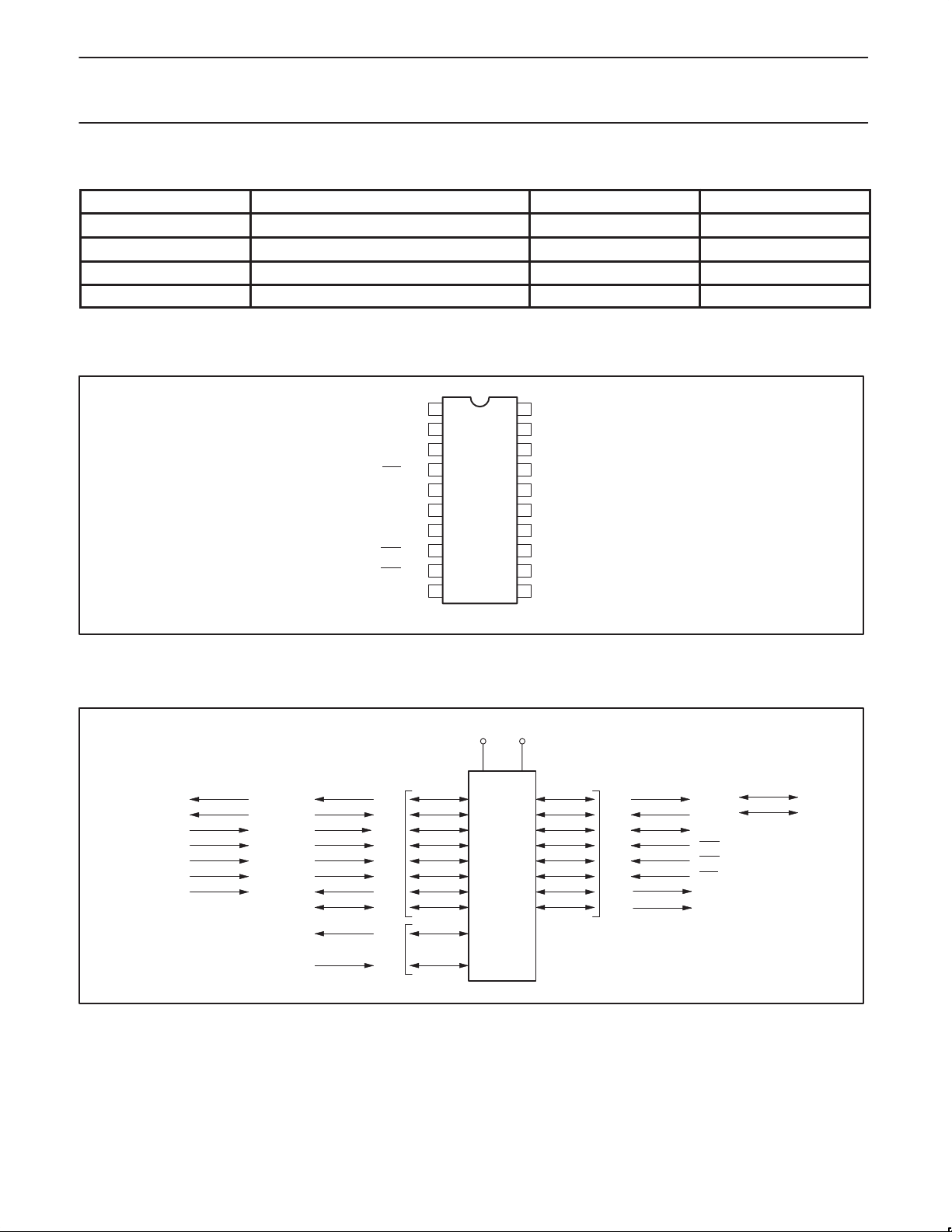
PIN CONFIGURATION, 20-PIN DIP AND SO PACKAGES
PWM3/CMP2/P0.0
PWM2/P1.7
PWM1/P1.6
RST
/P1.5
V
X1/P2.1
X2/CLKOUT/P2.0
/P1.4
INT1
SDA/INT0
/P1.3
SCL/T0/P1.2
1
2
3
4
5
SS
6
7
8
9
10
P0.1/CIN2B/PWM0
20
19
P0.2/CIN2A/BRAKE
18
P0.3/CIN1B/AD0
17
P0.4/CIN1A/AD1
16
P0.5/CMPREF/AD2
15
V
DD
14
P0.6/CMP1/AD3
13
P0.7/T1
12
P1.0/TxD
11
P1.1/RxD
87LPC768
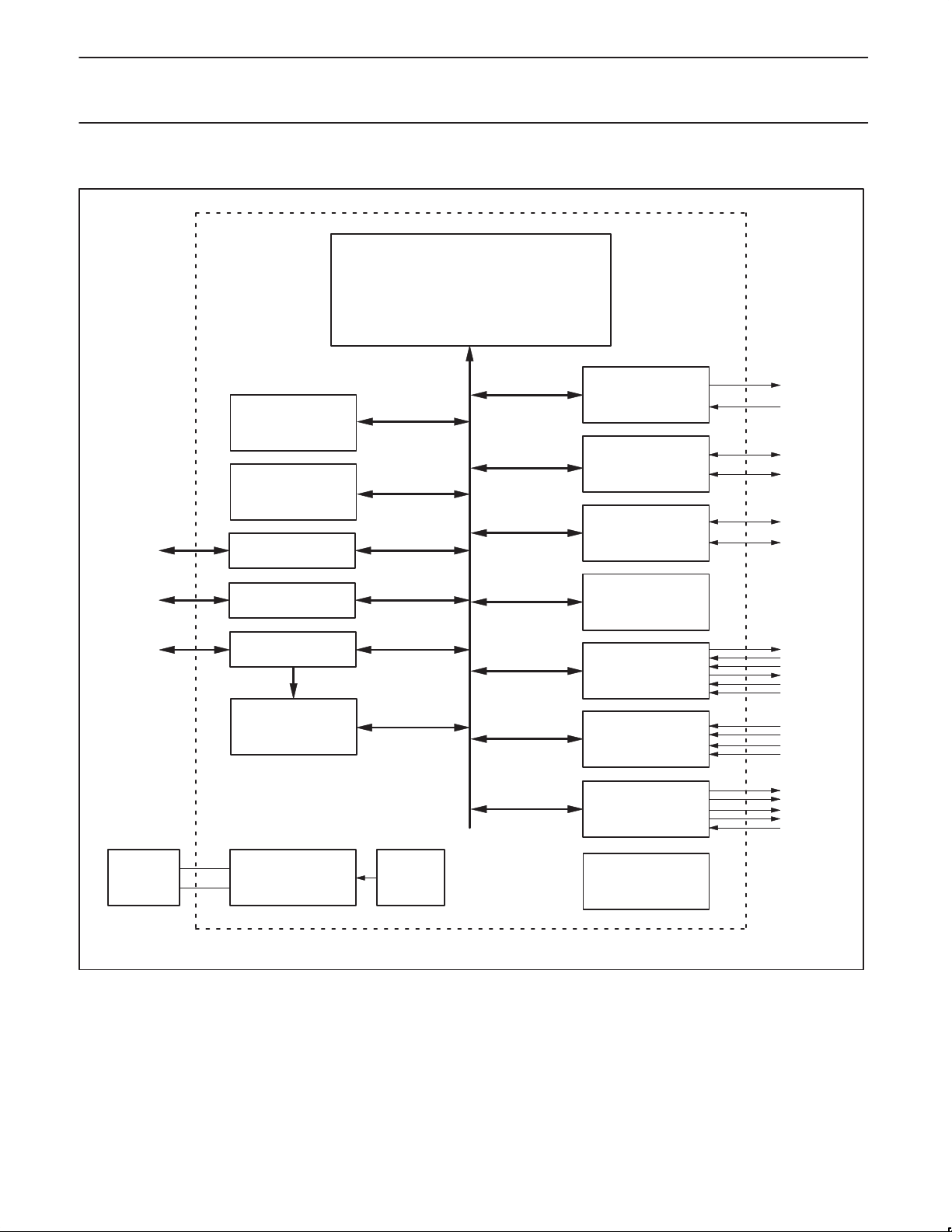
LOGIC SYMBOL
PWM3
PWM0
BRAKE
AD0
AD1
AD2
AD3
CIN2B
CIN2A
CIN1B
CIN1A
CMPREF
CMP1
CLKOUT/X2
SU01361
V
V
DD
SS
TxDCMP2
RxD
T0
INT0
PORT 0PORT 2
T1
X1
PORT 1
INT1
RST
PWM1
PWM2
SCL
SDA
SU01362
2000 May 02
2
Philips Semiconductors Preliminary specification
Low power, low price, low pin count (20 pin) microcontroller with
4 kB OTP 8-bit A/D, Pulse Width Modulator
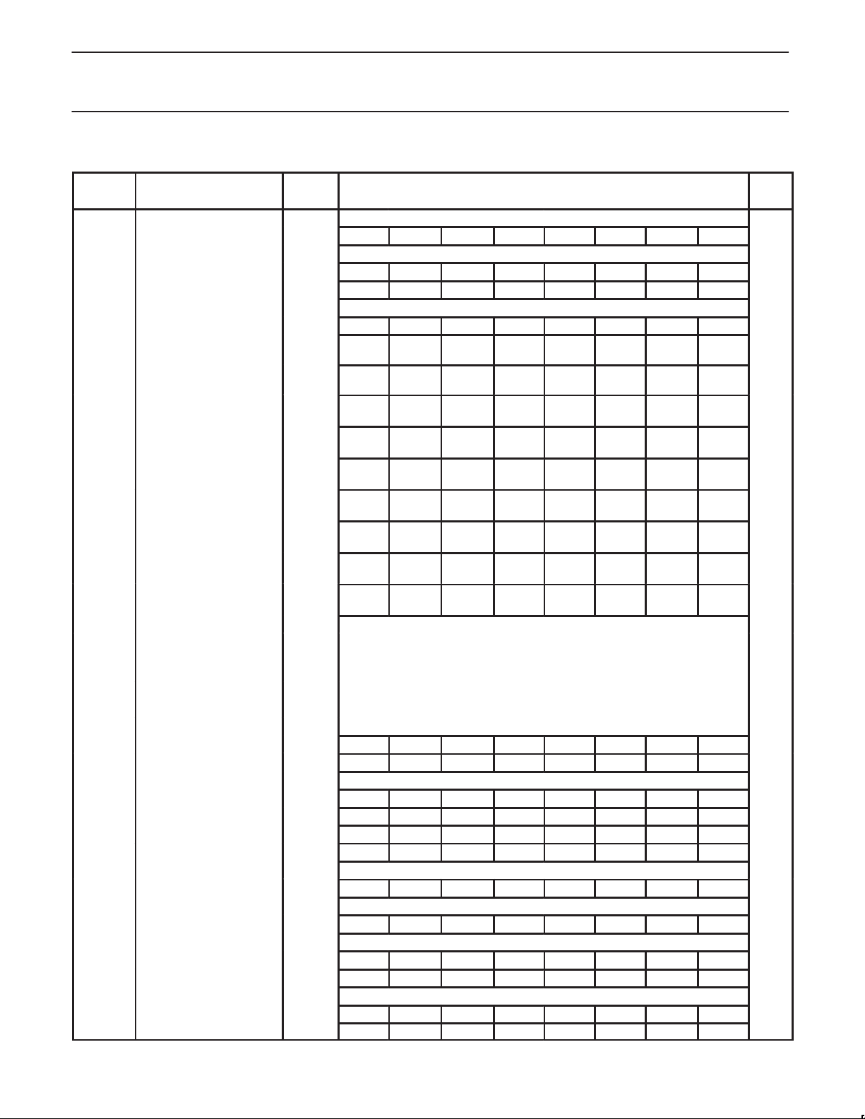
BLOCK DIAGRAM
ACCELERATED
80C51 CPU
INTERNAL BUS
4K BYTE
CODE EPROM
128 BYTE
DATA RAM
PORT 2
CONFIGURABLE I/OS
87LPC768
UART
I2C
TIMER 0, 1
CRYSTAL OR
RESONATOR
PORT 1
CONFIGURABLE I/OS
PORT 0
CONFIGURABLE I/OS
KEYPAD
INTERRUPT
CONFIGURABLE
OSCILLATOR
ON-CHIP
R/C
OSCILLATOR
WATCHDOG TIMER
AND OSCILLATOR
ANALOG
COMPARATORS
A/D
CONVERTER
PULSE WIDTH
MODULATOR
POWER MONITOR
(POWER-ON RESET,
BROWNOUT RESET)
SU01363
2000 May 02
3

Philips Semiconductors Preliminary specification
Low power, low price, low pin count (20 pin) microcontroller with
4 kB OTP 8-bit A/D, Pulse Width Modulator
FFFFh
UNUSED CODE
MEMORY SPACE
32-BYTE CUSTOMER
CODE SPACE
(ACCESSIBLE VIA MOVC)
UNUSED CODE
MEMORY SPACE
4 K BYTES ON-CHIP
CODE MEMORY
INTERRUPT VECTORS
ON-CHIP CODE
MEMORY SPACE
FCFFh
FCE0h
1000h
0FFFh
0000h
SPECIAL FUNCTION
REGISTERS
(ONLY DIRECTLY
ADDRESSABLE)
128 BYTES ON-CHIP DATA
MEMORY
(DIRECTLY AND
INDIRECTLY
ADDRESSABLE)
16-BIT ADDRESSABLE BYTES
ON-CHIP DATA
MEMORY SPACE
FFh
80h
7Fh
00h 0000h
87LPC768
UNUSED SPACE
CONFIGURATION BYTES
UCFG1, UCFG2
(ACCESSIBLE VIA MOVX)
UNUSED SPACE
EXTERNAL DATA
MEMORY SPACE*
FFFFh
FD01h
FD00h
* The 87LPC768 does not support access to external data memory. However, the User Configuration Bytes
are accessed via the MOVX instruction as if they were in external data memory.
Figure 1. 87LPC768 Program and Data Memory Map
SU01386
2000 May 02
4

Philips Semiconductors Preliminary specification
Low power, low price, low pin count (20 pin) microcontroller with
87LPC768
4 kB OTP 8-bit A/D, Pulse Width Modulator
PIN DESCRIPTIONS
MNEMONIC PIN NO. TYPE NAME AND FUNCTION
P0.0–P0.7 1, 13, 14,
P1.0–P1.7 2–4, 8–12 I/O Port 1: Port 1 is an 8-bit I/O port with a user-configurable output type, except for three pins as noted
16–20
1 O P0.0 CMP2 Comparator 2 output.
20 I P0.1 CIN2B Comparator 2 positive input B.
19 I P0.2 CIN2A Comparator 2 positive input A.
18 I P0.3 CIN1B Comparator 1 positive input B.
17 I P0.4 CIN1A Comparator 1 positive input A.
16 I P0.5 CMPREF Comparator reference (negative) input.
14 O P0.6 CMP1 Comparator 1 output.
13 I/O P0.7 T1 Timer/counter 1 external count input or overflow output.
12 O P1.0 TxD Transmitter output for the serial port.
11 I P1.1 RxD Receiver input for the serial port.
10 I/O
9 I
8 I P1.4 INT1 External interrupt 1 input.
4 I P1.5 RST External Reset input (if selected via EPROM configuration). A low on this pin
3 O P1.6 PWM1 Pulse Width Modulator 1 output
2 O P1.7 PWM2 Pulse Width Modulator 2 output
I/O Port 0: Port 0 is an 8-bit I/O port with a user-configurable output type. Port 0 latches are configured in
the quasi-bidirectional mode and have either ones or zeros written to them during reset, as determined
by the PRHI bit in the UCFG1 configuration byte. The operation of port 0 pins as inputs and outputs
depends upon the port configuration selected. Each port pin is configured independently. Refer to the
section on I/O port configuration and the DC Electrical Characteristics for details.
The Keyboard Interrupt feature operates with port 0 pins.
Port 0 also provides various special functions as described below.
PWM3 Pulse Width Modulator 3 output.
PWM0 Pulse Width Modulator 0 output.
BRAKE PWM brake input.
AD0 A/D channel 0 input.
AD1 A/D channel 1 input.
AD2 A/D channel 2 input.
AD3 A/D channel 3 input.
below. Port 1 latches are configured in the quasi-bidirectional mode and have either ones or zeros
written to them during reset, as determined by the PRHI bit in the UCFG1 configuration byte. The
operation of the configurable port 1 pins as inputs and outputs depends upon the port configuration
selected. Each of the configurable port pins are programmed independently. Refer to the section on I/O
port configuration and the DC Electrical Characteristics for details.
Port 1 also provides various special functions as described below.
I/O
I/O
P1.2 T0 Timer/counter 0 external count input or overflow output.
SCL I
P1.3 INT0 External interrupt 0 input.
SDA I2C serial data input/output. When configured as an output, P1.3 is open
2
C serial clock input/output. When configured as an output, P1.2 is open
drain, in order to conform to I
drain, in order to conform to I
resets the microcontroller, causing I/O ports and peripherals to take on their
default states, and the processor begins execution at address 0. When used
as a port pin, P1.5 is a Schmitt trigger input only.
2
C specifications.
2
C specifications.
2000 May 02
5

Philips Semiconductors Preliminary specification
Low power, low price, low pin count (20 pin) microcontroller with
87LPC768
4 kB OTP 8-bit A/D, Pulse Width Modulator
MNEMONIC NAME AND FUNCTIONTYPEPIN NO.
P2.0–P2.1 6, 7 I/O Port 2: Port 2 is a 2-bit I/O port with a user-configurable output type. Port 2 latches are configured in the
7 O P2.0 X2 Output from the oscillator amplifier (when a crystal oscillator option is
6 I P2.1 X1 Input to the oscillator circuit and internal clock generator circuits (when
V
SS
V
DD
5 I Ground: 0V reference.
15 I Power Supply: This is the power supply voltage for normal operation as well as Idle and
quasi-bidirectional mode and have either ones or zeros written to them during reset, as determined by
the PRHI bit in the UCFG1 configuration byte. The operation of port 2 pins as inputs and outputs
depends upon the port configuration selected. Each port pin is configured independently. Refer to the
section on I/O port configuration and the DC Electrical Characteristics for details.
Port 2 also provides various special functions as described below.
selected via the EPROM configuration).
CLKOUT CPU clock divided by 6 clock output when enabled via SFR bit and in
Power Down modes.
conjunction with internal RC oscillator or external clock input.
selected via the EPROM configuration).
2000 May 02
6
Philips Semiconductors Preliminary specification
Low power, low price, low pin count (20 pin) microcontroller with
87LPC768
4 kB OTP 8-bit A/D, Pulse Width Modulator
Table 1. Special Function Registers
Name Description
ACC* Accumulator E0h 00h
ADCON#* A/D Control C0h ENADC – – ADCI ADCS RCCLK AADR1 AADR0 00h
AUXR1# Auxiliary Function Register A2h KBF BOD BOI LPEP SRST 0 – DPS 02h
B* B register F0h 00h
CMP1#
CMP2#
CNSW0 PWM Counter Shadow
CNSW1 PWM Counter Shadow
CPSW0 PWM Compare Shadow
CPSW1 PWM Compare Shadow
CPSW2 PWM Compare Shadow
CPSW3 PWM Compare Shadow
CPSW4 PWM Compare Shadow
DAC0# A/D Result C5h 00h
DIVM#
DPTR: Data pointer (2 bytes)
DPH Data pointer high byte 83h 00h
DPL Data pointer low byte 82h 00h
I2CFG#* I2C configuration register C8h/RD SLA VEN MASTRQ 0 TIRUN – – CT1 CT0 00h
I2CON#* I2C control register D8h/RD RDA T ATN DRDY ARL STR STP
I2DAT# I2C data register D9h/RD RDA T 0 0 0 0 0 0 0 80h
IEN0* Interrupt enable 0 A8h EA EWD EBO ES ET1 EX1 ET0 EX0 00h
IEN1#* Interrupt enable 1 E8h ETI – EC1 EAD – EC2 EKB EI2 00h
IP0* Interrupt priority 0 B8h – PWD PBO PS PT1 PX1 PT0 PX0 00h
IP0H# Interrupt priority 0 high byte B7h – PWDH PBOH PSH PT1H PX1H PT0H PX0H 00h
IP1* Interrupt priority 1 F8h PTI – PC1 PAD – PC2 PKB PI2 00h
IP1H# Interrupt priority 1 high byte F7h PTIH – PC1H PADH – PC2H PKBH PI2H 00h
Comparator 1 control
register
Comparator 2 control
register
Register 0
Register 1
Register 0
Register 1
Register 2
Register 3
Register 4
CPU clock divide-by-M
control
SFR
Address
ACh – – CE1 CP1 CN1 OE1 CO1 CMF1 00h
ADh – – CE2 CP2 CN2 OE2 CO2 CMF2 00h
D1h CNSW7 CNSW6 CNSW5 CNSW4 CNSW3 CNSW2 CNSW1 CNSW0 FFh
D2h – – – – – – CNSW9 CNSW8 FFh
D3h CPSW07 CPSW06 CPSW05 CPSW04 CPSW03 CPSW02 CPSW01 CPSW00 00h
D4h CPSW17 CPSW16 CPSW15 CPSW14 CPSW13 CPSW12 CPSW11 CPSW10 00h
D5h CPSW27 CPSW26 CPSW25 CPSW24 CPSW23 CPSW22 CPSW21 CPSW20 00h
D6h CPSW37 CPSW36 CPSW35 CPSW34 CPSW33 CPSW32 CPSW31 CPSW30 00h
D7h CPSW39 CPSW38 CPSW29 CPSW28 CPSW19 CPSW18 CPSW09 CPSW08 00h
95h 00h
C8h/WR SLAVEN MASTRQ CLRTI TIRUN – – CT1 CT0
D8h/WR CXA IDLE CDR CARL CSTR CSTP XSTR XSTP
D9h/WR XDAT x x x x x x x
MSB LSB
E7 E6 E5 E4 E3 E2 E1 E0
C7 C6 C5 C4 C3 C2 C1 C0
F7 F6 F5 F4 F3 F2 F1 F0
CF CE CD CC CB CA C9 C8
DF DE DD DC DB DA D9 D8
AF AE AD AC AB AA A9 A8
EF EE ED EC EB EA E9 E8
BF BE BD BC BB BA B9 B8
FF FE FD FC FB FA F9 F8
Bit Functions and Addresses
MASTER
– 80h
Reset
Value
1
1
1
1
1
1
1
1
1
1
2000 May 02
7

Philips Semiconductors Preliminary specification
Low power, low price, low pin count (20 pin) microcontroller with
87LPC768
4 kB OTP 8-bit A/D, Pulse Width Modulator
Name
KBI# Keyboard Interrupt 86h 00h
P0* Port 0 80h T1 CMP1 CMPREF CIN1A CIN1B CIN2A CIN2B CMP2 Note 2
P1* Port 1 90h (P1.7) (P1.6) RST INT1 INT0 T0 RxD TxD Note 2
P2* Port 2 A0h – – – – – – X1 X2 Note 2
P0M1# Port 0 output mode 1 84h (P0M1.7) (P0M1.6) (P0M1.5) (P0M1.4) (P0M1.3) (P0M1.2) (P0M1.1) (P0M1.0) 00h
P0M2# Port 0 output mode 2 85h (P0M2.7) (P0M2.6) (P0M2.5) (P0M2.4) (P0M2.3) (P0M2.2) (P0M2.1) (P0M2.0) 00H
P1M1# Port 1 output mode 1 91h (P1M1.7) (P1M1.6) – (P1M1.4) – – (P1M1.1) (P1M1.0) 00h
P1M2# Port 1 output mode 2 92h (P1M2.7) (P1M2.6) – (P1M2.4) – – (P1M2.1) (P1M2.0) 00h
P2M1# Port 2 output mode 1 A4h P2S P1S P0S ENCLK T1OE T0OE (P2M1.1) (P2M1.0) 00h
P2M2# Port 2 output mode 2 A5h – – – – – – (P2M2.1) (P2M2.0) 00h
PCON Power control register 87h SMOD1 SMOD0 BOF POF GF1 GF0 PD IDL Note 3
PSW* Program status word D0h CY AC F0 RS1 RS0 OV F1 P 00h
PT0AD# Port 0 digital input disable F6h 00h
Description
SFR
Address
MSB LSB
87 86 85 84 83 82 81 80
97 96 95 94 93 92 91 90
A7 A6 A5 A4 A3 A2 A1 A0
D7 D6 D5 D4 D3 D2 D1 D0
Bit Functions and Addresses
Reset
Value
1
1
1
9F 9E 9D 9C 9B 9A 99 98
PWMCON0 PWM Control Register 0 DAh RUN XFER PWM3I PWM2I – PWM1I PWM0I – 00h
PWMCON1 PWM Control Register 1 DBh BKCH BKPS BPEN BKEN PWM3B PWM2B PWM1B PWM0B 00h
SCON* Serial port control 98h SM0 SM1 SM2 REN TB8 RB8 TI RI 00h
SBUF
SADDR# Serial port address register A9h 00h
SADEN# Serial port address enable B9h 00h
SP Stack pointer 81h 07h
TCON* Timer 0 and 1 control 88h TF1 TR1 TF0 TR0 IE1 IT1 IE0 IT0 00h
TH0 Timer 0 high byte 8Ch 00h
TH1 Timer 1 high byte 8Dh 00h
TL0 Timer 0 low byte 8Ah 00h
TL1 Timer 1 low byte 8Bh 00h
TMOD Timer 0 and 1 mode 89h GATE C/T M1 M0 GATE C/T M1 M0 00h
WDCON# Watchdog control register A7h – –
WDRST# Watchdog reset register A6h xxh
NOTES:
* SFRs are bit addressable.
# SFRs are modified from or added to the 80C51 SFRs.
1. Unimplemented bits in SFRs are X (unknown) at all times. Ones should not be written to these bits since they may be used for other
purposes in future derivatives. The reset value shown in the table for these bits is 0.
2. I/O port values at reset are determined by the PRHI bit in the UCFG1 configuration byte.
3. The PCON reset value is x x BOF POF–0 0 0 0b. The BOF and POF flags are not affected by reset. The POF flag is set by hardware upon
power up. The BOF flag is set by the occurrence of a brownout reset/interrupt and upon power up.
4. The WDCON reset value is xx11 0000b for a Watchdog reset, xx01 0000b for all other reset causes if the watchdog is enabled, and xx00
0000b for all other reset causes if the watchdog is disabled.
Serial port data buffer
register
99h xxh
8F 8E 8D 8C 8B 8A 89 88
WDOVF
WDRUN WDCLK WDS2 WDS1 WDS0 Note 4
2000 May 02
8

Philips Semiconductors Preliminary specification
Low power, low price, low pin count (20 pin) microcontroller with
4 kB OTP 8-bit A/D, Pulse Width Modulator
FUNCTIONAL DESCRIPTION
Details of 87LPC768 functions will be described in the following
sections.
Enhanced CPU
The 87LPC768 uses an enhanced 80C51 CPU which runs at twice the
speed of standard 80C51 devices. This means that the performance of
the 87LPC768 running at 5 MHz is exactly the same as that of a
standard 80C51 running at 10 MHz. A machine cycle consists of 6
oscillator cycles, and most instructions execute in 6 or 12 clocks. A
user configurable option allows restoring standard 80C51 execution
timing. In that case, a machine cycle becomes 12 oscillator cycles.
In the following sections, the term “CPU clock” is used to refer to the
clock that controls internal instruction execution. This may
sometimes be different from the externally applied clock, as in the
case where the part is configured for standard 80C51 timing by
means of the CLKR configuration bit or in the case where the clock
is divided down via the setting of the DIVM register. These features
are described in the Oscillator section.
Analog Functions
The 87LPC768 incorporates analog peripheral functions: an Analog
to Digital Converter and two Analog Comparators. In order to give
the best analog function performance and to minimize power
consumption, pins that are being used for analog functions must
have the digital outputs and inputs disabled.
Digital outputs are disabled by putting the port output into the Input
Only (high impedance) mode as described in the I/O Ports section.
Digital inputs on port 0 may be disabled through the use of the
PT0AD register. Each bit in this register corresponds to one pin of
Port 0. Setting the corresponding bit in PT0AD disables that pin’s
digital input. Port bits that have their digital inputs disabled will be
read as 0 by any instruction that accesses the port.
device has a very limited number of pins, the A/D power supply and
references are shared with the processor power pins, V
The A/D converter operates down to a V
The A/D converter circuitry consists of a 4-input analog multiplexer
and an 8-bit successive approximation ADC. The A/D employs a
ratiometric potentiometer which guarantees DAC monotonicity.
The A/D converter is controlled by the special function register
ADCON. Details of ADCON are shown in Figure 2. The A/D must be
enabled by setting the ENADC bit at least 10 microseconds before a
conversion is started, to allow time for the A/D to stabilize. Prior to
the beginning of an A/D conversion, one analog input pin must be
selected for conversion via the AADR1 and AADR0 bits. These bits
cannot be changed while the A/D is performing a conversion.
An A/D conversion is started by setting the ADCS bit, which remains
set while the conversion is in progress. When the conversion is
complete, the ADCS bit is cleared and the ADCI bit is set. When
ADCI is set, it will generate an interrupt if the interrupt system is
enabled, the A/D interrupt is enabled (via the EAD bit in the IE1
register), and the A/D interrupt is the highest priority pending
interrupt.
When a conversion is complete, the result is contained in the
register DAC0. This value will not change until another conversion is
started. Before another A/D conversion may be started, the ADCI bit
must be cleared by software. The A/D channel selection may be
changed by the same instruction that sets ADCS to start a new
conversion, but not by the same instruction that clears ADCI.
The connections of the A/D converter are shown in Figure 3.
The ideal A/D result may be calculated as follows:
Result + (VIN–VSS)x
87LPC768
and VSS.
supply of 3.0V .
DD
256
(round result to the nearest integer)
–V
V
DD
SS
DD
Analog to Digital Converter
The 87LPC768 incorporates a four channel, 8-bit A/D converter. The
A/D inputs are alternate functions on four port 0 pins. Because the
2000 May 02
9

Philips Semiconductors Preliminary specification
Low power, low price, low pin count (20 pin) microcontroller with
87LPC768
4 kB OTP 8-bit A/D, Pulse Width Modulator
ADCON Address: C0h
Bit addressable
Reset Value: 00h
BIT SYMBOL FUNCTION
ADCON.7 ENADC When ENADC = 1, the A/D is enabled and conversions may take place. Must be set 10
ADCON.6 - Reserved for future use. Should not be set to 1 by user programs.
ADCON.5 - Reserved for future use. Should not be set to 1 by user programs.
ADCON.4 ADCI A/D conversion complete/interrupt flag. This flag is set when an A/D conversion is completed.
ADCON.3 ADCS A/D start. Setting this bit by software starts the conversion of the selected A/D input. ADCS
ADCI, ADCS
0 0 A/D not busy, a conversion can be started.
0 1 A/D busy, the start of a new conversion is blocked.
1 0 An A/D conversion is complete. ADCI must be cleared prior to starting a new conversion.
1 1 An A/D conversion is complete. ADCI must be cleared prior to starting a new conversion. This
ADCON.2 RCCLK When RCCLK = 0, the CPU clock is used as the A/D clock. When RCCLK = 1, the internal RC
ADCON.1, 0 AADR1,0 Along with AADR0, selects the A/D channel to be converted. These bits can only be written
AADR1, AADR0
0 0 AD0 (P0.3).
0 1 AD1 (P0.4).
1 0 AD2 (P0.5).
1 1 AD3 (P0.6).
76543210
ENADC - - ADCI ADCS RCCLK AADR1 AADR0
microseconds before a conversion is started. ENADC cannot be cleared while ADCS or ADCI
are 1.
This bit will cause a hardware interrupt if enabled and of sufficient priority. Must be cleared by
software.
remains set while the A/D conversion is in progress and is cleared automatically upon
completion. While ADCS or ADCI are one, new start commands are ignored.
A/D Status
state exists for one machine cycle as an A/D conversion is completed.
oscillator is used as the A/D clock. This bit is writable while ADCS and ADCI are 0.
while ADCS and ADCI are 0.
A/D Input Selected
SU01354
Figure 2. A/D Control Register (ADCON)
A/D Timing
The A/D may be clocked in one of two ways. The default is to use
the CPU clock as the A/D clock source. When used in this manner,
the A/D completes a conversion in 31 machine cycles. The A/D may
be operated up to the maximum CPU clock rate of 20 MHz, giving a
conversion time of 9.3 µs. The formula for calculating A/D
conversion time when the CPU clock runs the A/D is: 186 µs / CPU
clock rate (in MHZ). To obtain accurate A/D conversion results, the
CPU clock must be at least 1 MHz.
The A/D may also be clocked by the on-chip RC oscillator, even if
the RC oscillator is not used as the CPU clock. This is accomplished
by setting the RCCLK bit in ADCON. This arrangement has several
advantages. First, the A/D conversion time is faster at lower CPU
clock rates. Also, the CPU may be run at speeds below 1 MHz
without affecting A/D accuracy. Finally, the Power Down mode may
be used to completely shut down the CPU and its oscillator, along
2000 May 02
with other peripheral functions, in order to obtain the best possible
A/D accuracy. This should not be used if the MCU uses an external
clock source greater than 4 MHz.
When the A/D is operated from the RCCLK while the CPU is running
from another clock source, 3 or 4 machine cycles are used to
synchronize A/D operation. The time can range from a minimum of 3
machine cycles (at the CPU clock rate) + 108 RC clocks to a
maximum of 4 machine cycles (at the CPU clock rate) + 112 RC
clocks.
Example A/D conversion times at various CPU clock rates are
shown in Table 2. In Table 2, maximum times for RCCLK = 1 use an
RC clock frequency of 4.5 MHz (6 MHz - 25%). Minimum times for
RCCLK = 1 use an RC clock frequency of 7.5 MHz (6 MHz + 25%).
Nominal time assume an ideal RC clock frequency of 6 MHz and an
average of 3.5 machine cycles at the CPU clock rate.
10

Philips Semiconductors Preliminary specification
CPU Clock Rate
RCCLK = 0
Low power, low price, low pin count (20 pin) microcontroller with
4 kB OTP 8-bit A/D, Pulse Width Modulator
Table 2. Example A/D Conversion Times
RCCLK = 1
minimum nominal maximum
32 kHz NA 563.4 µs 659 µs 757 µs
1 MHz 186 µs 32.4 µs 39.3 µs 48.9 µs
4 MHz 46.5 µs 18.9 µs 23.6 µs 30.1 µs
11.0592 MHz 16.8 µs 16 µs 20.2 µs 27.1 µs
12 MHz 15.5 µs
16 MHz 11.6 µs
20 MHz 9.3 µs
Note: Do not clock ADC from the RC oscillator when MCU clock is greater than 4 MHz.
V
+ = V
AD0 (P0.3)
AD1 (P0.4)
AD2 (P0.5)
AD3 (P0.6)
00
01
10
11
A/D Converter
REF
V
REF
- = V
DD
SS
87LPC768
AADR1
AADR0
ADCON
Figure 3. A/D Converter Connections
The A/D in Power Down and Idle Modes
While using the CPU clock as the A/D clock source, the Idle mode
may be used to conserve power and/or to minimize system noise
during the conversion. CPU operation will resume and Idle mode
terminate automatically when a conversion is complete if the A/D
interrupt is active. In Idle mode, noise from the CPU itself is
eliminated, but noise from the oscillator and any other on-chip
peripherals that are running will remain.
The CPU may be put into Power Down mode when the A/D is
clocked by the on-chip RC oscillator (RCCLK=1). This mode gives
the best possible A/D accuracy by eliminating most on-chip noise
sources.
If the Power Down mode is entered while the A/D is running from the
CPU clock (RCCLK=0), the A/D will abort operation and will not
wake up the CPU. The contents of DAC0 will be invalid when
operation does resume.
DAC0
(A/D result)
SU01356
When an A/D conversion is started, Power Down or Idle mode must
be activated within two machine cycles in order to have the most
accurate A/D result. These two machine cycles are counted at the
CPU clock rate. When using the A/D with either Power Down or Idle
mode, care must be taken to insure that the CPU is not restarted by
another interrupt until the A/D conversion is complete. The possible
causes of wakeup are different in Power Down and Idle modes.
A/D accuracy is also affected by noise generated elsewhere in the
application, power supply noise, and power supply regulation. Since
the 87LPC768 power pins are also used as the A/D reference and
supply, the power supply has a very direct affect on the accuracy of
A/D readings. Using the A/D without Power Down mode while the
clock is divided through the use of CLKR or DIVM has an adverse
effect on A/D accuracy.
2000 May 02
11

Philips Semiconductors Preliminary specification
Low power, low price, low pin count (20 pin) microcontroller with
87LPC768
4 kB OTP 8-bit A/D, Pulse Width Modulator
Code Examples for the A/D
The first piece of sample code shows an example of port configuration for use with the A/D. This example sets up the pins so that all four A/D
channels may be used. Port configuration for analog functions is described in the section Analog Functions.
; Set up port pins for A/D conversion, without affecting other pins.
mov PT0AD,#78h ; Disable digital inputs on A/D input pins.
anl P0M2,#87h ; Disable digital outputs on A/D input pins.
orl P0M1,#78h ; Disable digital outputs on A/D input pins.
Following is an example of using the A/D with interrupts. The routine ADStart begins an A/D conversion using the A/D channel number supplied
in the accumulator. The channel number is not checked for validity. The A/D must previously have been enabled with sufficient time to allow for
stabilization.
The interrupt handler routine reads the conversion value and returns it in memory address ADResult. The interrupt should be enabled prior to
starting the conversion.
; Start A/D conversion.
ADStart:
orl ADCON,A ; Add in the new channel number.
setb ADCS ; Start an A/D conversion.
; orl PCON,#01h ; The CPU could be put into Idle mode here.
; orl PCON,#02h ; The CPU could be put into Power Down mode here if RCCLK = 1.
ret
; A/D interrupt handler.
ADInt:
push ACC ; Save accumulator.
mov A,DAC0 ; Get A/D result,
mov ADResult,A ; and save it in memory.
clr ADCI ; Clear the A/D completion flag.
anl ADCON,#0fch ; Clear the A/D channel number.
pop ACC ; Restore accumulator.
reti
Following is an example of using the A/D with polling. An A/D conversion is started using the channel number supplied in the accumulator . The
channel number is not checked for validity. The A/D must previously have been enabled with suf ficient time to allow for stabili zation. The
conversion result is returned in the accumulator.
ADRead:
orl ADCON,A ; Add in the new channel number.
setb ADCS ; Start A/D conversion.
ADChk:
jnb ADCI,ADChk ; Wait for ADCI to be set.
mov A,DAC0 ; Get A/D result.
clr ADCI ; Clear the A/D completion flag.
anl ADCON,#0fch ; Clear the A/D channel number.
ret
2000 May 02
12

Philips Semiconductors Preliminary specification
Low power, low price, low pin count (20 pin) microcontroller with
4 kB OTP 8-bit A/D, Pulse Width Modulator
Analog Comparators
Two analog comparators are provided on the 87LPC768. Input and
output options allow use of the comparators in a number of different
configurations. Comparator operation is such that the output is a
logical one (which may be read in a register and/or routed to a pin)
when the positive input (one of two selectable pins) is greater than
the negative input (selectable from a pin or an internal reference
voltage). Otherwise the output is a zero. Each comparator may be
configured to cause an interrupt when the output value changes.
Comparator Configuration
Each comparator has a control register, CMP1 for comparator 1 and
CMP2 for comparator 2. The control registers are identical and are
shown in Figure 4.
CMPn
Address: ACh for CMP1, ADh for CMP2
Not Bit Addressable
The overall connections to both comparators are shown in Figure 5.
There are eight possible configurations for each comparator, as
determined by the control bits in the corresponding CMPn register:
CPn, CNn, and OEn. These configurations are shown in Figure 6.
The comparators function down to a V
When each comparator is first enabled, the comparator output and
interrupt flag are not guaranteed to be stable for 10 microseconds.
The corresponding comparator interrupt should not be enabled
during that time, and the comparator interrupt flag must be cleared
before the interrupt is enabled in order to prevent an immediate
interrupt service.
87LPC768
of 3.0V .
DD
Reset Value: 00h
01234567
COnOEnCNnCPnCEn——
CMFn
BIT SYMBOL FUNCTION
CMPn.7, 6 — Reserved for future use. Should not be set to 1 by user programs.
CMPn.5 CEn Comparator enable. When set by software, the corresponding comparator function is enabled.
CMPn.4 CPn Comparator positive input select. When 0, CINnA is selected as the positive comparator input. When
CMPn.3 CNn Comparator negative input select. When 0, the comparator reference pin CMPREF is selected as
CMPn.2 OEn Output enable. When 1, the comparator output is connected to the CMPn pin if the comparator is
CMPn.1 COn Comparator output, synchronized to the CPU clock to allow reading by software. Cleared when the
CMPn.0 CMFn Comparator interrupt flag. This bit is set by hardware whenever the comparator output COn changes
Comparator output is stable 10 microseconds after CEn is first set.
1, CINnB is selected as the positive comparator input.
the negative comparator input. When 1, the internal comparator reference V
negative comparator input.
enabled (CEn = 1). This output is asynchronous to the CPU clock.
comparator is disabled (CEn = 0).
state. This bit will cause a hardware interrupt if enabled and of sufficient priority. Cleared by
software and when the comparator is disabled (CEn = 0).
Figure 4. Comparator Control Registers (CMP1 and CMP2)
is selected as the
ref
SU01152
2000 May 02
13

Philips Semiconductors Preliminary specification
Low power, low price, low pin count (20 pin) microcontroller with
4 kB OTP 8-bit A/D, Pulse Width Modulator
COMPARATOR 1
+
–
COMPARATOR 2
+
–
CO1
OE1
CHANGE DETECT
CO2
OE2
CHANGE DETECT
(P0.4) CIN1A
(P0.3) CIN1B
(P0.5) CMPREF
(P0.2) CIN2A
(P0.1) CIN2B
CP1
V
ref
CN1
CP2
CN2
CMF1
87LPC768
CMP1 (P0.6)
INTERRUPT
CMP2 (P0.0)
CINnA
CMPREF
CINnA
Vref (1.23V)
CINnB
CMPREF
CPn, CNn, OEn = 0 0 0
+
–
CPn, CNn, OEn = 0 1 0
+
–
CPn, CNn, OEn = 1 0 0
+
–
Figure 5. Comparator Input and Output Connections
COn
COn
COn
CINnA
CMPREF
CINnA
V
(1.23V)
ref
CINnB
CMPREF
CMF2
CPn, CNn, OEn = 0 0 1
+
COn
–
CPn, CNn, OEn = 0 1 1
+
COn
–
CPn, CNn, OEn = 1 0 1
+
COn
–
INTERRUPT
SU01153
CMPn
CMPn
CMPn
2000 May 02
CPn, CNn, OEn = 1 1 0
CINnB
V
(1.23V) V
ref
+
COn
–
Figure 6. Comparator Configurations
14
CINnB
(1.23V)
ref
CPn, CNn, OEn = 1 1 1
+
COn
–
CMPn
SU01154

Philips Semiconductors Preliminary specification
Low power, low price, low pin count (20 pin) microcontroller with
4 kB OTP 8-bit A/D, Pulse Width Modulator
Internal Reference Voltage
An internal reference voltage generator may supply a default
reference when a single comparator input pin is used. The value of
the internal reference voltage, referred to as V
Comparator Interrupt
Each comparator has an interrupt flag CMFn contained in its
configuration register . This flag is set whenever the comparator
output changes state. The flag may be polled by software or may be
used to generate an interrupt. The interrupt will be generated when
the corresponding enable bit ECn in the IEN1 register is set and the
interrupt system is enabled via the EA bit in the IEN0 register.
Comparators and Power Reduction Modes
Either or both comparators may remain enabled when Power Down
or Idle mode is activated. The comparators will continue to function
in the power reduction mode. If a comparator interrupt is enabled, a
change of the comparator output state will generate an interrupt and
CmpInit:
mov PT0AD,#30h ; Disable digital inputs on pins that are used
anl P0M2,#0cfh ; Disable digital outputs on pins that are used
orl P0M1,#30h ; for analog functions: CIN1A, CMPREF.
mov CMP1,#24h ; Turn on comparator 1 and set up for:
call delay10us ; The comparator has to start up for at
anl CMP1,#0feh ; Clear comparator 1 interrupt flag.
setb EC1 ; Enable the comparator 1 interrupt. The
setb EA ; Enable the interrupt system (if needed).
ret ; Return to caller.
, is 1.28 V ±10%.
ref
; for analog functions: CIN1A, CMPREF.
; – Positive input on CIN1A.
; – Negative input from CMPREF pin.
; – Output to CMP1 pin enabled.
; least 10 microseconds before use.
; priority is left at the current value.
Figure 7.
wake up the processor. If the comparator output to a pin is enabled,
the pin should be configured in the push-pull mode in order to obtain
fast switching times while in power down mode. The reason is that
with the oscillator stopped, the temporary strong pull-up that
normally occurs during switching on a quasi-bidirectional port pin
does not take place.
Comparators consume power in Power Down and Idle modes, as
well as in the normal operating mode. This fact should be taken into
account when system power consumption is an issue.
Comparator Configuration Example
The code shown in Figure 7 is an example of initializing one
comparator. Comparator 1 is configured to use the CIN1A and
CMPREF inputs, outputs the comparator result to the CMP1 pin,
and generates an interrupt when the comparator output changes.
The interrupt routine used for the comparator must clear the
interrupt flag (CMF1 in this case) before returning.
87LPC768
SU01189
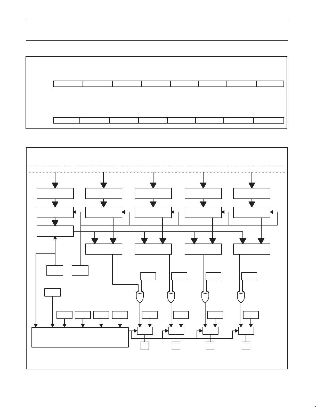
Pulse Width Modulator
The 87LPC768 contains four Pulse Width Modulated (PWM)
channels which generate pulses of programmable length and
interval. The output for PWM0 is on P0.1, PWM1 on P1.6, PWM2
on P1.7 and PWM3 on P0.1. After chip reset the internal output of
the each PWM channel is a “1.” Note that the state of the pin will
not reflect this if UCFG1.5, PRHI, is set to a zero. In this case
before the pin will reflect the state of the internal PWM output a “1”
must be written to each port bit that serves as a PWM output. A
block diagram is shown in Figure 8.
The interval between successive outputs is controlled by a 10–bit
down counter which uses the internal microcontroller clock as its
input. When bit 3 in the UCFG1 register is a “1” the microcontroller
2000 May 02
clock, and therefore the PWM counter clock, has the same
frequency as the clock source defined by the FOSC bits in UCFG1.
When bit 3 in the UCFG1 register is a “0” the microcontroller and
PWM counter clocks operate at half the frequency of clock source
defined by the FOSC bits in UCFG1. When the counter reaches
underflow it is reloaded with a user selectable value. This
mechanism allows the user to set the PWM frequency at any integer
sub–multiple of the microcontroller clock frequency. The repetition
frequency of the PWM is given by:
f
= FC / (CNSW+1)
PWM
where CNSW is contained in CNSW0 and CNSW1 as described in
the following tables.
15
Philips Semiconductors Preliminary specification
Low power, low price, low pin count (20 pin) microcontroller with
4 kB OTP 8-bit A/D, Pulse Width Modulator
CNSW0: Counter Shadow register 0
Addr: 0D1H
Reset Value: FFH
76543210
CNSW7 CNSW6 CNSW5 CNSW4 CNSW3 CNSW2 CNSW1 CNSW0
CNSW1: Counter Shadow register 1
Addr: 0D2H
Reset Value: FFH
76 54321 0
Unused Unused Unused Unused Unused Unused CNSW9 CNSW8
The word “Shadow” in the above refers to the fact that writes are not
into the register that controls the counter; rather they are into a
holding register. As described below the transfer of data from this
INTERNAL BUS
holding register, into the register which contains the actual reload
value, is controlled by the user’s program.
87LPC768
10 BIT SHADOW
REGISTER
10 BIT COUNTER
REGISTER
10 BIT COUNTER
RUN XFER
BRAKE
BKCH BKPS BPEN BKEN
BRAKE CONTROL LOGIC
10 BIT SHADOW
REGISTER
10 BIT COMPARE
REGISTER
AB AB AB AB
A>B A>B A>B A>B
10 BIT SHADOW
REGISTER
10 BIT COMPARE
REGISTER
PWM3I
PWM3B
2:1 MUX
PWM2I
PWM2B
2:1 MUX
10 BIT SHADOW
REGISTER
10 BIT COMPARE
REGISTER
PWM1I
PWM1B
2:1 MUX
10 BIT SHADOW
REGISTER
10 BIT COMPARE
REGISTER
PWM0I
PWM0B
2:1 MUX
2000 May 02
PWM3
PWM2
Figure 8. PWM Block Diagram
16
PWM1
PWM0
SU01364

Philips Semiconductors Preliminary specification
Low power, low price, low pin count (20 pin) microcontroller with
4 kB OTP 8-bit A/D, Pulse Width Modulator
The width of each PWM output pulse is determined by the value in
the appropriate compare shadow registers, CPSW0 through
CPSW4, CPSW0–3 for bits 0–7 and CPSW4 for bits 7 and 8. When
the counter described above reaches underflow the PWM output is
forced high. It remains high until the compare value is reached at
which point it goes low until the next underflow. The number of
microcontroller clock pulses that the PWM
by:
t
= (CNSW – CPSWn+1)
HI
A compare value greater than the counter reload value results in the
PWM output being permanently high. In addition there are two
CPSW0: Compare Shadow register 0
Addr: 0D3H
Reset Value: 00H
765432 1 0
CPSW07 CPSW06 CPSW05 CPSW04 CPSW03 CPSW02 CPSW01 CPSW00
CPSW1: Compare Shadow register 1
Addr: 0D4H
Reset Value: 00H
765432 1 0
CPSW17 CPSW16 CPSW15 CPSW14 CPSW13 CPSW12 CPSW11 CPSW10
output is high is given
n
special cases. A compare value of all zeroes, 000, causes the
output to remain permanently high. A compare value of all ones,
3FF, results in the PWM output remaining permanently low. Again
the compare value is loaded into a shadow register. The transfer
from this holding register to the actual compare register is under
program control.
The register assignments are shown below where the number
immediately following “CPSW” identifies the PWM output. Thus
CPSW0 controls the width of PWM0, CPSW1 the width of PWM1
etc. In the case of two digits following “CPSW,” e.g. CPSW00, the
second digit refers to the bit of the compare value. Thus CPSW00
represents the value loaded into bit 0 of the PWM0 compare register
87LPC768
CPSW2: Compare Shadow register 2
Addr: 0D5H
Reset Value: 00H
765432 1 0
CPSW27 CPSW26 CPSW25 CPSW24 CPSW23 CPSW22 CPSW21 CPSW20
CPSW3: Compare Shadow register 3
Addr: 0D6H
Reset Value: 00H
765432 1 0
CPSW37 CPSW36 CPSW35 CPSW34 CPSW33 CPSW32 CPSW31 CPSW30
CPSW4: Compare Shadow register 4
Addr: 0D7H
Reset Value: 00H
765432 1 0
CPSW39 CPSW38 CPSW29 CPSW28 CPSW19 CPSW18 CPSW09 CPSW08
The overall functioning of the PWM module is controlled by the
contents of the PWMCON0 register. The operation of most of the
control bits is straightforward. For example there is an invert bit for
each output which causes results in the output to have the opposite
value compared to its non-inverted output. The transfer of the data
from the shadow registers to the control registers is controlled by the
PWMCON0.6 while PWMCON0.7 allows the PWM to be either in
the run or idle state. The user can monitor when underflow causes
the transfer to occur by monitoring the Transfer bit, PWCON0.6.
When the transfer takes place the PWM logic automatically resets
this bit.
The fact that the transfer from the shadow to the working registers
only occurs when there is an underflow in the counter results in the
need for the user’s program to observe the following precautions. If
PWMCON1 is written with Transfer set without Run being enabled
the transfer will never take place. Thus if a subsequent write sets
Run without Transfer the compare and counter values will not be
those expected. If Transfer and Run are set, and prior to underflow
there is a subsequent load of PWMCON0 which sets Run but not
Transfer, the transfer will never take place. Again the compare and
counter values that existed prior to the update attempt will be used.
As outlined above the Transfer bit can be polled to determine when
the transfer occurs. Unless there is a compelling reason to do
otherwise, it is recommended that both Run, PWMCON0.7, and
Transfer, PWMCON0.7, be set when PWMCON0 is written.
When the Run bit, PWMCON0.7, is cleared the PWM outputs take
on the state they had just prior to the bit being cleared. In general
this state is not known. In order to place the outputs in a known
2000 May 02
17

Philips Semiconductors Preliminary specification
Low power, low price, low pin count (20 pin) microcontroller with
87LPC768
4 kB OTP 8-bit A/D, Pulse Width Modulator
state when Run is cleared the Compare registers can be written to
either the “always 1” or “always 0” so the output will have the output
desired when the counter is halted. After this PWMCON0 should be
written with the Transfer and Run bits are enabled. After this is
done PWMCON0 to is polled to find that the Transfer has taken
place. Once the transfer has occurred the Run bit in PWMCON0
can be cleared. The outputs will retain the state they had just prior
to the Run being cleared. If the Brake pin (see discussion below in
PWMCON0: PWM Control register 0
Addr: 0DAH
Reset Value: 00H
BIT SYMBOL FUNCTION
PWMCON0.7 RUN 0= Counter Halted & Preset Value loaded. If Brake is asserted, PWMx output will be equal to the
PWMCON0.6 XFER 0= Counter & Compare shadow registers are not connected to the active registers
PWMCON0.5 PWM3I 0= PWM3 output is non–inverted. Output is a ‘1’ from the start of the cycle until compare; ’0’
PWMCON0.4 PWM2I 0= PWM2 output is non–inverted. Output is a ‘1’ from the start of the cycle until compare; ’0’
PWMCON0.2 PWM1I 0= PWM1 output is non–inverted. Output is a ‘1’ from the start of the cycle until compare; ’0’
PWMCON0.1 PWM0I 0= PWM0 output is non–inverted. Output is a ‘1’ from the start of the cycle until compare; ’0’
76543210
RUN XFER PWM3I PWM2I – PWM1I PWM0I –
value of the corresponding PWMxB bit (PWMCON1[3:0]). If Brake is not asserted, PWMx
output will be equal to the Value after compare
1= Counter run
1= Shadow register contents transferred to active registers, at the next Counter underflow This bit
is auto–cleared by hardware after the data transfer from shadow to active registers
thereafter.
1= PWM3 output is inverted. Output is a ‘0’ from the start of the cycle until compare; ’0’ thereafter.
thereafter.
1= PWM2 output is inverted. Output is ‘0’ from the start of the cycle until compare; ’1’ thereafter.
thereafter.
1= PWM1 output is inverted. Output is ‘0’ from the start of the cycle until compare; ’1’ thereafter.
thereafter.
1= PWM0 output is inverted. Output is ‘0’ from the start of the cycle until compare; ’1’ thereafter.
section concerning the operation of PWMCON1) is not used to
control the brake function, the “Brake when not running” function can
be used to cause the outputs to have a given state when the PWM
is halted. This approach should be used only in time critical
situations when there is not sufficient time to use the approach
outlined above since going from the Brake state to run without
causing an undefined state on the outputs is not straightforward. A
discussion on this topic is included in the section on PWMCON1.
The Brake function, which is controlled by the contents of the
PWMCON1 register, is somewhat unique. In general when Brake is
asserted the four PWM outputs are forced to a user selected state,
namely the state selected by PWMCON1 bits 0 to 3.
As shown in the description of the operation of the PWMCON1
register if PWMCON1.4 is a “1” brake is asserted under the control
PWMCON1.7, BKCH, and PWMCON1.5, BPEN. As shown if both
are a “0” Brake is asserted. If PWMCON1.7 is a “1” brake is
asserted when the run bit, PWMCON0.7, is a “0.” If PWMCON1.6 is
a “1” brake is asserted when the Brake Pin, P0.2, has the same
polarity as PWMCON1.6. When brake is asserted in response to
this pin the RUN bit, PWMCON0.7, is automatically cleared. The
combination of both PWMCON1.7 and PWMCON1.5 being a “1” is
not allowed.
Since the Brake Pin being asserted will automatically clear the Run
bit, PWMCON0.7, the user program can poll this bit to determine
when the Brake Pin causes a brake to occur. The other method for
detecting a brake caused by the Brake Pin would be to tie the Brake
Pin to one of the external interrupt pins. This latter approach is
2000 May 02
SU01387
needed if the Brake signal can be of insufficient length to ensure
that it can be captured by a polling routine.
When, after being asserted, the condition causing the brake is
removed, the PWM outputs go to whatever state that had
immediately prior to the brake. This means that in order to go from
brake being asserted to having the PWM run without going through
an indeterminate state care must be taken. If the Brake Pin causes
brake to be asserted the following prototype code will allow the
PWM to go from brake to run smoothly.
•Rewrite PWMCON1 to change from Brake Pin enabled to S/W
Brake
•Write CPSW.(0:4) to always “1”, 11 h, or always “0” 00 h, to give
brake pattern
•Set PWMCON0 to enable Run and Transfer.
•Poll Brake Pin until it is no longer active. When no longer active:
18
 Loading...